HAL Id: hal-01403868
https://hal.archives-ouvertes.fr/hal-01403868
Submitted on 28 Nov 2016
HAL is a multi-disciplinary open access
archive for the deposit and dissemination of
sci-entific research documents, whether they are
pub-lished or not. The documents may come from
teaching and research institutions in France or
abroad, or from public or private research centers.
L’archive ouverte pluridisciplinaire HAL, est
destinée au dépôt et à la diffusion de documents
scientifiques de niveau recherche, publiés ou non,
émanant des établissements d’enseignement et de
recherche français ou étrangers, des laboratoires
publics ou privés.
Improving spatial resolution of immunity maps by
post-processing
Alexandre Boyer
To cite this version:
Alexandre Boyer. Improving spatial resolution of immunity maps by post-processing. 2016 Asia-Pacific
International Symposium on Electromagnetic Compatibility and Signal Integrity (APEMC2016), May
2016, Shenzhen, China. pp.56 - 59, �10.1109/APEMC.2016.7522794�. �hal-01403868�
Improving Spatial Resolution of Immunity Maps by
Post-Processing
A. Boyer
CNRS, LAAS, 7 avenue du colonel Roche, F-31400 Toulouse, France Univ. de Toulouse, INSA, LAAS, F-31400 Toulouse, France
alexandre.boyer @laas.fr
Abstract— Near-field injection is a promising method for the
analysis of the susceptibility of electronic boards and circuits. The resulting immunity map provides a precise localization of the sensitive area to electromagnetic disturbances. A major requirement is the spatial resolution of the immunity map. This paper aims at proposing a post-processing method to enhance the spatial resolution of immunity map and validating it on case studies at board and integrated circuit levels.
Keywords— Near-Field Scan; Immunity; Resolution enhancement; Plane Wave Spectrum Theory.
I. INTRODUCTION
Near-field scan is a well-established method for the diagnosis of EMC problems at printed circuit board (PCB) and integrated circuit (IC) levels. It consists in measuring the local electric (E) or magnetic (H) fields with a miniature receiving probe for a root-cause analysis of emission issues. The method can be reversed to apply local electromagnetic disturbances and is known as near-field injection. A near-field probe is placed in the vicinity of an electronic device and excited by a disturbance signal in order to induce a local intense E or H field. The coupling of the field may induce enough large voltage fluctuations across a PCB or an IC under test to trigger failures [1] - [2]. Both methods provide 2D cartography or map of the local emission (emission map) or amplitude of the failure induced by the probe according to its position (immunity map).
The quality of the diagnosis depends on the spatial resolution of the map, i.e. the ability to locate the source of a near-field emission or the coupling area accurately. The resolution depends on the distance between the probe and the circuit under test but also on the dimensions of the probe. Due to its finite size, the probe produces a significant field over a relatively large volume which couples over a large area of the device under test (DUT). Huge efforts are done to reduce near-field probe dimensions and thus improve the resolution. However, the drawback of the miniaturization is either the degradation of receiving probe sensitivity, or the reduction of the field produced by the injection probe. Recently, numerous research works have been led to improve the resolution of emission cartography by post-processing methods. They consist in compensating the receiving characteristics of the measurement probe and extracting the actual undisturbed field distribution. Three types of method have been proposed: plane
wave spectrum (PWS) theory [3], image restoration techniques based on Wiener filtering [4] and Neural network based post-processing [5]. The resolution of emission scan are considerably improved even when the measurement is done with large receiving probes. However, this type of post-processing methods has never been used to improve the resolution of immunity scan. Contrary to emission scan post-processing, the main purpose is to extract the receiving characteristic of the device under test, in order to improve the localization of coupling area to near-field disturbances produced by a large injection probe. This paper proposes to reuse PWS theory in order to improve the resolution of immunity scan, and demonstrate its validity on practical case studies at PCB and IC levels.
II. POST-PROCESSING PRINCIPLE
Let us consider a near-field injection probe excited by a sinusoidal signal which produces an electric or magnetic field F in any point (xs,ys) of a 2D horizontal plane at a constant
distance or scan altitude hs above the DUT. The field is
supposed known and undisturbed by nearby objects. This 2D distribution is called the spatial profile of the field F. The result of a near-field injection scan on a PCB or IC is a 2D immunity map which provides for each probe position (xp, yp)
placed at the scan altitude hs above the DUT its response S to
the near-field disturbance produced by the probe. The immunity map provides an indirect and distorted picture of the coupling area of the incoming disturbance, because the probe produces a significant field over a large surface of the DUT. Depending on the scan altitude and the probe dimensions, the resolution of the immunity map may be insufficient to locate precisely where the incoming disturbance couples on the DUT. The spatial profile of the DUT response S is related to the field F by a DUT property called the receiving characteristic R (1), which depends only on DUT geometry. It quantifies the response of the DUT to one particular component of the field F produced by the injection probe placed in (xp,yp). Thus, this term provides a direct information
about the coupling area and the sensitivity of the DUT to the disturbances produced by the near-field injection probe.
(
)
(
)
(
p s p s)
(
s s)
s s p p p p dy dx y x F y y x x R y x F R y x S∫∫
− − = ∗ = , , , , (1)This work is supported by the French Agence Nationale de la Recherche under contract ANR-12-INSE-005 E-Mata-Hari.
Determining R is more convenient in spectral domain than spatial domain representation. The transformation is based on the PWS theory. The field is decomposed into a superposition of an infinite number of plane waves propagating in x and y directions with wave numbers kx and ky. The relation between
spatial and spectral domain representations of the field is ensured by a 2D Fourier transform in the xy plane, as given by (2) and (3) where subscript F~denotes the spectral domain
representation.
(
)
=∫ ∫
−+∞∞(
)
− − dxdy e e e z y x F z k k F~ x, y, , , jωt jkxx jkyy (2)(
)
=∫ ∫
−+∞∞(
)
x y y jk x jk t j y x k ze e e dk dk k F z y x F ω x y π , , ~ 4 1 , , 2 (3)With the spectral domain representation, (1) is rewritten in the following form. The receiving characteristic is the ratio between the DUT response and the field emitted by the probe.
(
) (
(
)
)
z
k
k
F
z
k
k
S
z
k
k
R
y x y x y x,
,
~
,
,
~
,
,
~
=
(4)In practice, the extraction of the receiving characteristic consists in five steps:
1. Acquisition of the immunity map of the DUT S(xp,yp,-hs) with a given injection probe
2. Extraction of the spatial profile of the field produced by the injection probe F(xs,ys) by measurement or
simulation
3. Computation of S~ and F~ by a 2D FFT
4. Computation of R~ according to (4) 5. Computation of R by an inverse 2D FFT.
In practice, various sources of errors degrade the accuracy of this method. First, the result is affected by systematic errors on probe positioning, measured or simulated spatial profiles of disturbing field and DUT response. Secondly, the result is sensitive to measurement noise. To reduce the random noise influence, the noisy wave number components, i.e. with an amplitude less than an arbitrary signal-to-noise ratio constraint, are filtered out. Thirdly, as the number of spatial samples is finite, truncation errors affect the FFT results. The induced oscillations (Gibbs effect) may be reduced by applying windowing such as Blackman window. Finally, if the influence of the DUT on the injection probe characteristics is not negligible, the spatial profile of the field produced by the injection probe may become erroneous.
III. VALIDATION OF THE METHOD ON PCBTRACE
A. Description of the test structures
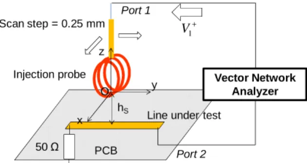
In order to validate the method, the coupling between a short microstrip line and a miniature magnetic field probe is performed, according to the experimental set-up described in Fig. 1. x y z hS Injection probe O
Line under test
Vector Network Analyzer Port 1 Port 2 + 1 V Scan step = 0.25 mm PCB 50 Ω
Fig. 1. Measurement of the coupling between the injection probe and a PCB trace
The coupling coefficient between the injection probe and the line under test is measured at a fixed scan altitude according to the probe position. The microstrip line is 0.15 mm wide and 1 mm long. The injection probe consists in a 2 mm large three turn coil. The magnetic field produced by the probe has been characterized by measurements and validated by simulation previously.
Fig. 2 compares the 2D map of the coupling coefficient between the injection probe and the line under test (the immunity map S), and the computed 2D map of the receiving characteristic R of the line. The result is obtained at 300 MHz for a scan altitude hs = 1 mm. Their values are normalized to
simplify the comparison. Both maps show a main lobes above the line, but the lobe observed on receiving characteristic map is narrower. The spatial resolution is quatified as the width at half maximum of the main lobe. The resolutions of the measured voltage and receiving characteristic profiles are equal to 2.5 and 0.75 mm respectively in Y direction, and 4.5 and 1.5 mm in X direction. This result demonstrates that the receiving characteristic profile improves the localization of the coupling area of the near-field disturbance.
Immunity map (S) x y Receiving characteristic (R) x y
Fig. 2. (Top): 2D map of the coupling coefficient between the injection probe and the line under test; (Bottom): Receiving characteristic of the line under test
IV. VALIDATION OF THE METHOD ON INTEGRATED CIRCUIT
The previous methodology is now applied on an integrated circuit in order to improve the localization of disturbed package pins or circuit interconnects. The experiments are
performed on a test-chip designed with Freescale® in 0.25 µm SMARTMOS 8 technology with 4 metal layers [6]. On-chip sensor (OCS) are disseminated within the test chip to reconstruct the time domain profile of the local voltage fluctuations induced by the near-field injection. The OCS is able to measure the waveform of voltage bounces across non accessible nodes with a precise time resolution, a large bandwidth and a low intrusivity. The acquisition principle is explained in [7]. Previous near-field injections have been performed on this circuit, showing a significant coupling of the tangential magnetic field component [8].
Fig. 3 presents the experimental setup in order to measure the voltage coupled to the circuit and extract its receiving characteristic. The injection probe presented in part III is reused for this test. It is displaced above the test chip and excited by a 200 MHz sinusoidal RF source. A sensor connected on an internal interconnect terminated by 50 Ω
loads is used to monitor the voltage fluctuation induced in the circuit according to the injection probe position. The signal acquired by the OCS is then transmitted through a dedicated output to an external acquisition card and post-processed to provide the time-domain profile of the voltage measured by the sensor. PCB x y z hS Injection probe O
Circuit under test
+ 1 V Scan step = 0.1 mm Acquisition card RF disturbance source S y n c h ro n iz a ti o n OCS Sensor output
Fig. 3. Measurement setup of the voltage coupled on the test-chip by the injection probe
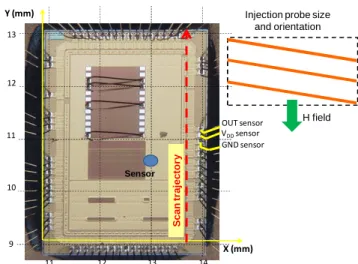
The injection scan is done above one side of the die. The position of the scan and sensor bonding wires is shown in Fig. 4. The size of the probe is also reported for comparison purpose with the die surface. The probe is placed at 700 µ m above the IC die surface. The scan step is set to 0.11 mm.
X (mm) Y (mm) 12 13 14 9 10 11 12 13 11
Injection probe size and orientation H field S c a n t ra je c to ry Sensor OUT sensor VDDsensor GND sensor
Fig. 4. Position of the near-field scan above the IC die surface
The evolution of the voltage measured by the sensor and the extracted receiving characteristic according to the probe position are compared in Fig. 5. Coupled voltage and receiving characteristic spatial profiles present a main lobe with width half maxima equal to 3 and 1 mm respectively. The resolution of the receiving characteristic profile is three times better than that of the induced voltage profile. The main lobe of the coupled voltage profile is almost as wide as the die so that the localization of the coupling area is not precise. In contrary, the main lobe of the receiving characteristics is centered above the three bonding wires associated to the sensor. However, the resolution is not sufficient to identify clearly the bonding wire responsible of the coupling, since their separation is about 150 µm.
Fig. 5. Comparison between the spatial profile of voltage induced on the circuit under test and its receiving characteristic
V. CONCLUSION
Near-field injection is a promising method for the analysis of the susceptibility of electronic cards and integrated circuits. The precise localization of sensitive area of a device under test depends on the spatial resolution of the immunity map resulting from the scan. This paper has shown that miniaturizing injection probe is not the only method to improve the resolution of immunity map. A post-processing method has been proposed to extract the receiving characteristic of the device under test to improve the spatial resolution. Examples at PCB and IC levels presented in this
paper show that it may provide a two or threefold improvement of the spatial resolution. We insist that this method is not an alternative to the miniaturization of injection probe. As this miniaturization effort leads to a reduction of the produced disturbing field, it constitutes an additional method to improve the resolution of immunity map obtained with relatively large injection probe.
References
[1] O. Kroning, M. Krause, M. Leone, "Near field-Immunity Scan on Printed Circuit Board Level", in Proc. SPI, 2010, pp. 101-102. [2] A. Boyer, E. Sicard, S. Bendhia, « Characterization of the
Electromagnetic Susceptibility of Integrated Circuits using a Near Field Scan », Electronic Letters, vol. 43, no. 1, pp. 15-16, 4th Jan. 2007. [3] J. Shi, M. A. Cracraft, K. P. Slattery, M. Yamaguchi, R. E. DuBroff,
"Calibration and Compensation of Near-Field Scan Measurements",
IEEE Trans. on Electromagnetic Compatibility, vol. 47, no 3, August 2005.
[4] A. Tankielun, U. Keller, W. John, H. Garbe, "Complex Deconvolution for Improvement of Standard Monopole Near-Field Measurement Results", 16th Int. EMC Zurich Symposium, February 2005.
[5] R. Brahimi, A. Kornaga, M. Bensetti, D. Baudry, Z. Riah, A. Louis, B. Mazari, "Postprocessing of Near-Field Measurement Based on Neural Networks", IEEE Transactions on Instrumentation and Measurement, vol. 60, no 2, February 2011.
[6] SmartmosTM Technology - Process Information, more information on
/www.nxp.com/files/technology_manufacturing/doc/SMARTMOS_FA CT_SHEET.pdf
[7] S. Ben Dhia, A. Boyer, B. Vrignon, M. Deobarro, T. V. Dinh, “On-Chip Noise Sensor for Integrated Circuit Susceptibility Investigations”, IEEE Trans. on Instrumentation and Measurement, vol. 61, no. 3, pp. 696-707, Mar. 2012.
[8] A. Boyer, B. Vrignon, M. Cavarroc, "Modeling Magnetic Near-Field Injection at Silicon Die Level", IEEE Transaction on Electromagnetic Compatibility, vol. 58, no 1, February 2016, pp. 257-268, 10.1109/TEMC.2015.2486041.