HAL Id: hal-02542043
https://hal.archives-ouvertes.fr/hal-02542043
Submitted on 7 Jul 2020HAL is a multi-disciplinary open access archive for the deposit and dissemination of sci-entific research documents, whether they are pub-lished or not. The documents may come from teaching and research institutions in France or abroad, or from public or private research centers.
L’archive ouverte pluridisciplinaire HAL, est destinée au dépôt et à la diffusion de documents scientifiques de niveau recherche, publiés ou non, émanant des établissements d’enseignement et de recherche français ou étrangers, des laboratoires publics ou privés.
Pushing absorption of perovskite nanocrystals into the
infrared
Prachi Rastogi, Audrey Chu, Charlie Gréboval, Junling Qu, Ulrich
Nguétchuissi Noumbé, Sang-Soo Chee, Mayank Goyal, Adrien Khalili
Lazarjani, Xiang Zhen Xu, Hervé Cruguel, et al.
To cite this version:
Prachi Rastogi, Audrey Chu, Charlie Gréboval, Junling Qu, Ulrich Nguétchuissi Noumbé, et al.. Pushing absorption of perovskite nanocrystals into the infrared. Nano Letters, American Chemical Society, 2020, 20 (5), pp.3999-4006. �10.1021/acs.nanolett.0c01302�. �hal-02542043�
Pushing Absorption of Perovskite Nanocrystals into the Infrared
Prachi Rastogi,
1$Audrey Chu
1$, Charlie Gréboval
1, Junling Qu
1, Ulrich Nguétchuissi Noumbé
2,
Sang-Soo Chee
1, Mayank Goyal
1, Adrien Khalili
1, Xiang Zhen Xu
3, Hervé Cruguel
1, Sandrine
Ithurria
3, Bruno Gallas
1, Jean-Francois Dayen
2, Lenart Dudy
4, Mathieu G. Silly
4, Gilles Patriarche
5,
Aloyse Degiron
6, Gregory Vincent
7, Emmanuel Lhuillier
1*1
Sorbonne Université, CNRS, Institut des NanoSciences de Paris, INSP, F-75005 Paris, France.
2Université de Strasbourg, IPCMS-CMRS UMR 7504, 23 Rue du Loess, 67034 Strasbourg,
France.
3
Laboratoire de Physique et d’Etude des Matériaux, ESPCI-Paris, PSL Research University,
Sorbonne Université Univ Paris 06, CNRS UMR 8213, 10 rue Vauquelin 75005 Paris, France.
4
Synchrotron-SOLEIL, Saint-Aubin, BP48, F91192 Gif sur Yvette Cedex, France.
5
Centre de Nanosciences et de Nanotechnologies, CNRS, University of Paris-Sud, Université
Paris-Saclay,
C2N, Marcoussis 91460, France.
6
Université de Paris, CNRS, Laboratoire Matériaux et Phénomènes Quantiques, 75013 Paris,
France.
7
ONERA - The French Aerospace Lab, 6, chemin de la Vauve aux Granges, BP 80100, F-91123
Palaiseau, France.
Abstract: To date defect-tolerance electronic structure of Lead halide perovskite nanocrystals is limited to optical feature in the visible range. Here, we demonstrate that IR sensitization of formamidinium lead iodine (FAPI) nanocrystals array can be obtained by its doping with PbS nanocrystals. In this hybrid array, absorption comes from the PbS nanocrystals while transport is driven by the perovskite which reduces the dark current compared to pristine PbS. In addition, we fabricate a field-effect transistor using a high capacitance ionic glass made of hybrid FAPI/PbS nanocrystal arrays. We show that the hybrid material has an n-type nature with an electron mobility of 2 x 10⁻³ cm2 V-1s-1. However, the dark current reduction is mostly
balanced by a loss of absorption. To overcome this limitation, we couple the FAPI/PbS hybrid to a guided mode resonator, that can enhance the infrared light absorption.
Keywords: Perovskites, Formamidinium lead iodine, nanocrystal, short-wave infrared, light matter-coupling, resonator.
$ These two authors have equal contributions.
Beyond their bright luminescence in the visible, nanocrystals (NCs) have raised interest for the design of optoelectronic devices and especially for infrared (IR) sensors.1–3 Particularly, lead chalcogenides have attracted much attention for the design of solar cells collecting the near infrared (NIR) part of the solar spectrum.4–6 However, over the recent years, solar cells based on PbS colloidal quantum dots (CQDs) have been challenged by the growing competition of perovskite materials. While PbS CQD solar cells achieved competitive short circuit current, the trap states lead to a reduced open circuit voltage7,8 (0.6 V which is half
of the band gap), limiting their power conversion efficiency.
Lead halide perovskites present a defect-tolerant electronic structure, which accommodate the presence of dangling bonds on the NC surface. This property facilitates solar cells with large open circuit voltage9–11 (>1 V) and leads to high photoluminescence efficiencies without shells passivating the surface.12,13 In spite of this
success, the band gap of lead halide perovskite solar cells remains large which prevents the absorption of the NIR part of the solar spectrum. Alternatively, replacing lead by tin allows to reduce the band gap, but it also reduced the material stability.14 So far, reducing the band gap of perovskite materials to enable their
absorption in the IR range appears as a major limitation in the field.
To address the IR spectrum using formamidinium lead iodine (FAPI) perovskite NCs we incorporate PbS NCs. The strategy of mixing PbS CQDs with thin films (bulk) of perovskite has already been explored,15–17 either to push the absorption18–23 of the material toward the IR or as a way to achieve NIR light emitting diodes.24 Here, we use an all-nanocrystals-based approach and push the final material absorption up to the
short-wave IR (1.5 µm at the absorption peak). By pushing the IR sensitization toward longer wavelength (1.7 µm) compared to previous work (around 1.2 µm ), we can anticipate a higher role of the interface band offset between the two materials.15–23 In addition, coupling of PbS CQD with perovskite (bulk) matrix was achieved via epitaxial connection between two materials16; and thus wave function in the PbS was leaking into the
perovskite, affecting the optical spectrum. Here, by mixing two population we can independently tune their band gap. To benefit from such hybrid structures, the loss of absorption originated from the FAPI needs to be balanced by lower dark current. To reach this goal, we demonstrate that the ratio of FAPI needs to be above the percolation threshold of the PbS CQDs. In this case, the transport is driven by the “wide” band gap of FAPI that reduces the dark current with respect to pristine PbS.
To probe transport in this hybrid material, we use a field-effect transistor (FET) configuration. However, so far there is no report for perovskite NCs based FET. Conventional dielectrics have been unsuccessful to displace the Fermi level close to the valence and conduction band likely due to the Fermi level position located at the middle of the gap.25,26 Alternative attempts based on electrolyte gating result in the dissolution
of the ionic perovskite NCs. Here, we use a high capacitance gate made of ionic glass, enabling us for the first time to extract the field effect mobility of a perovskite NCs film. Finally, we introduce a plasmonic resonator based on guided modes to improve the IR absorption in FAPI/PbS hybrid film. Introduction of such guided mode resonators27 (GMRs) not only enhances the absorption of the film above the one of pristine
PbS, but also generates electrical gain.28 We are thus able to improve the detectivity by one order of
We demonstrate IR sensitization of a perovskite NC array by doping them with PbS NCs. FAPI has been selected as the perovskite host matrix. This choice is a good trade-off between the material stability and the band gap value. The latter needs to be larger than the one of the IR absorbing PbS NCs to reduce the thermally activated carrier density associated with dark current. However, a wide band gap will prevent an efficient charge transfer from the IR sensitizer to the perovskite host matrix due to the presence of large energy offset. FAPI is synthesized using the procedure given by references24,29, leading to a 750 nm (1.65
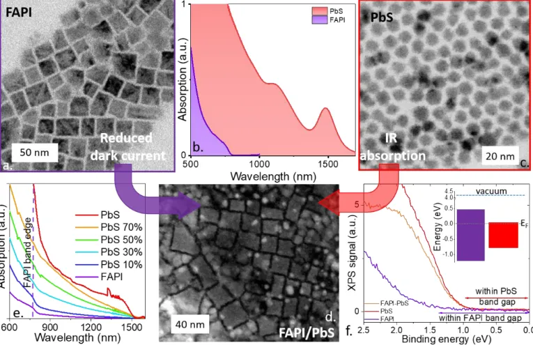
eV) band edge energy, with a bulk like absorption spectrum, see Figure 1b. The FAPI particles show a cubic shape according to transmission electron microscopy (Figure 1a).
PbS NCs are grown30 with a band edge appearing at 1.5 µm (0.82 eV), which is slightly bluer than the targeted
detection wavelength (1.55 µm) to account for the redshift occurring when the material is processed under film form and its ligands are stripped off. PbS NCs have a spherical shape, see transmission electron microscopy (TEM) image in Figure 1c.
When a fresh solution of FAPI is mixed with PbS NCs, we observe an absorption (Figure 1e) which presents contribution from the two materials with both an edge in the short wave infrared (SWIR) at 1.5 µm and a slope disruption resulting from the FAPI host matrix around 750 nm. This confirms that the two materials are preserved after mixing. Electron microscopy (Figure 1d) and energy dispersive X-ray spectroscopy (Figure S1 and S2) results also support the mixing of the two materials at the nanoscale.
Figure 1 a Transmission electron microscopy (TEM) image of FAPI NCs. b. Absorption spectra of FAPI and PbS NCs . c TEM image of PbS NCs with a band edge at 1500 nm (after synthesis). d. High angle annular dark field TEM image of a FAPI/PbS mixture. FAPI have a characteristic square shape, while PbS are small spheres. e. Absoprtion spectra of FAPI/PbS mixture with various PbS ratios. f. Photoemission signal relative to the valence band for FAPI, PbS and FAPI/PbS (35% PbS content). Inset is a band diagram for FAPI and PbS NCs. The Fermi energy is set at 0 eV.
To further explore the electronic structure of the hybrid material, we use X-ray photoemission spectroscopy. A complete analysis of the core levels for the pristine material and the hybrid material is given in Figure S3-8. No shift of the core level binding energy has been noticed, revealing that (i) material integrity is preserved after mixing and (ii) no charge transfer occurs between the two materials under dark condition.
The PbS prepared under such condition is found to be quasi n-type degenerated31 (i.e. Fermi level lies very
close to the conduction band), while for FAPI the Fermi level is deep into the band gap.24 We determine it
here to be located on the n-side (i.e. upper part of the conduction band) suggesting some degree of fluctuation from sample to sample. The band alignment between PbS and FAPI is found to be type I, see the inset of Figure 1f. The probing of the valence band state by photoemission clearly indicates that the valence band state in the mixture corresponds to PbS, see Figure 1f.
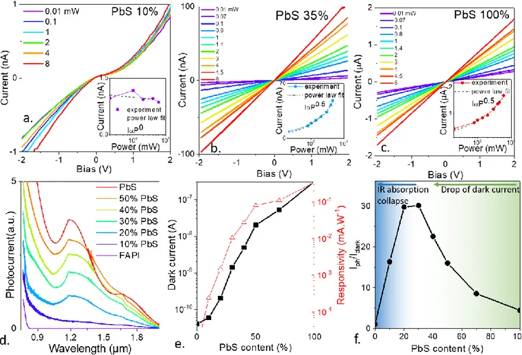
We then deposit the materials onto electrodes in order to measure their transport properties and demonstrate the IR sensitization of the perovskites. The ligands of the hybrid material are exchanged by dipping the film into a solution of lead acetate in ethyl acetate.10,23 I-V curves under illumination at 1.55 µm are given in Figure
2a-c for various PbS content. As expected from its band gap value, the pristine PbS is photoconductive under IR illumination (Figure 2c). Similarly, when the PbS ratio becomes low, almost no current modulation is obtained in the IR (Figure 2a). This picture is consistent with the photon energy (0.8 eV) being smaller that the band gap of the perovskite (1.65 eV). For intermediate PbS content, we observe a clear IR photocurrent modulation (Figure 2b). The PbS content also affects the material time response and we found that the very low PbS content has a slow response, consistent with bolometric effect. Once PbS is introduced, the response fastens, see Figure S9 and S10, but while the pristine PbS also presents a slow contribution (likely from traps), the hybrid response only presents a single fast contribution. To confirm that the response is induced by the PbS absorber, we measure the photocurrent of the hybrid material for various PbS contents and we clearly observe that the IR photoconduction follows the absorption of PbS, see Figure 2d.
Figure 2 a. I-V curves under illumination for a low (10%) PbS content film made of FAPI/PbS NCs. The inset provides the power dependence of the photocurrent. b. I-V curves under illumination for an intermediate (35%) PbS content film made of FAPI/PbS NCs. The inset provides the power dependence of the photocurrent. c. I-V curves under illumination for a PbS NC film. The inset provides the power dependence of the photocurrent. d Photocurrent spectra for films made of FAPI/PbS NCs with various PbS contents. e. Dark current and responsivity as a function of the PbS content for films made of FAPI/PbS NCs. f. Ratio of the photocurrent over the dark current for films made of FAPI/PbS nanocrystals as a function of the PbS content. For part a-c, e and f, the illumination is done by a 1.55 µm laser diode.
In Figure 2e and f, we follow how the dark conduction, the responsivity and the light to dark current ratio are influenced by the PbS content in the FAPI host matrix. Two regimes are clearly observed. When FAPI is introduced into pure PbS, we observe a reduction of the dark conductance, due to the wider band gap nature of FAPI which has less thermally activated carriers. The material also contains less absorbers which lead to a decrease of the responsivity. Nevertheless, responsivity does not drop as fast as the dark current. At very low PbS content, the IR absorption becomes too weak due to the lack of absorbing dopants. As a result, there is an optimal doping value, maximizing the light to dark current modulation, see Figure 2f. The latter being around 35%. In the following, this PbS ratio will be used for the hybrid material.
To further understand the electronic structure and charge transfer into this hybrid material, we then design a FET configuration. While FET has been reported for perovskite thin films,32–34 this tool is still lacking for perovskite NCs.
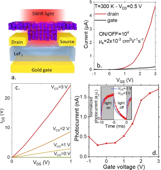
Figure 3 a Scheme of a field effect transistor based on a LaF3 substrate used as gate and channel made of
a FAPI/PbS (35% PbS content) NC thin film. b Transfer curves (drain and gate current as a function of the applied gated bias under a constant drain source bias set equal to 0.5 V) for the device described in part a. c. I-V curves with different gate biases for the device described in part a. d. Photocurrent (λ = 1.55 µm-P= 4 mW) as a function of the applied gate bias for the device described in a. The inset is plot of the current as a function of time as the light is turned on and off for two values of the applied gate bias. The drain source bias is set at 0.5 V.
To obtain a high capacitance gate we use an approach based on ionic glass. In such glass, the application of an electric field on the substrate can displace vacancies to the surface of the material and generates a polarization.35 Here, we utilize a LaF
3 glass which has been successful for the gating of 2D materials36–38 and
narrow band gap NCs films.39,40 This gating approach combines two key advantages with respect to the
colloidal perovskite material. First, it is a high capacitance (400 nF.cm-2) method,36 with a sheet capacitance
from electrolyte gating. It consequently allows to strongly modulate the relative position of the band with respect to the Fermi level. Second, it is an all solid-state approach which prevents the perovskite from any exposition to dissolving solvent.
Using this approach, we obtain a FET which scheme is depicted in Figure 3a and whose channel is made of a perovskite NC film doped with IR absorber. The hybrid material appears to have the n-type nature according to the transfer curve, see Figure 3b and c and S11. The on-off ratio reaches four orders of magnitude. For the sake of comparison, for pristine PbS NCs with the same gate, an ambipolar behavior was reported with a two orders of magnitude current modulation.36 This change indicates the filtering effect of the perovskite
which allows the electron transfer while preventing the hole transfer. This picture is consistent with the band alignment obtained from photoemission. The Schottky barrier for the electron transferred into the perovskites is weaker than that of the hole. We have determined also the electron mobility to be 2x10⁻³ cm2.V-1s-1. Such
value was still lacking for perovskite NC arrays. It gives an idea of the inter-nanoparticle coupling in a ligand-exchanged array of perovskites NCs. The obtained value is close to the one obtained for conventional solid-state metal chalcogenides NCs,41,42 but remains weaker than state of the art value obtained for phase transfer
ligand exchanges using ionic surface chemistry.43,44
Interestingly, not only the dark conductance can be modulated thanks to the gate but also does the photocurrent. The magnitude of the photocurrent can be tuned by a factor of 5 with the gate bias, see Figure 3d. Also note that the magnitude enhancement of the photoresponse comes at the price of a slower response, see the inset of Figure 3d. In this sense, the tunability of the photoresponse is made at quasi constant gain-bandwidth product as commonly observed in NCs-based phototransistors.37,45
We have developed a hybrid material absorbing in the IR, where the dark current is reduced compared to the pristine IR material. However, the absorption of the hybrid material is reduced (typically by a factor of 3) compared to the pristine IR material. To overcome this absorption drop, we introduce a plasmonic resonator,46,47 whose role is to enhance the incident electromagnetic field onto the thin slab of absorbing
material. We choose to use a guided mode resonator (GMR).27,48,49 The resonator will generate a mode which
propagates along the film thus enabling multi passes of the light through the absorbing semiconductor which enhances the light absorption.
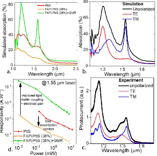
Our GMR is composed of a back-side mirror, which role is particularly to generate a second pass of the light. On the top of the mirror a dielectric spacer and a gold grating are deposited, see Figure 4a for a scheme of the device. The gold grating plays a dual role. First (i), it generates a resonance for a wavelength equal to the period of the grating times the optical index of the semiconductor. Here the targeted wavelength is 1.55 µm, which corresponds to a grating period of ≈1 µm assuming an optical index of 1.6 for the hybrid material, see supporting information for more details about the design (Figure S12-15 and S17) and fabrication (Figure S16) of the grating. Note that the value of 1.6 reflects the presence of the perovskite host matrix since the value of 2 is better fitting in the case of pristine PbS. Secondly, (ii) this grating is used as interdigitated electrodes for transport.
Figure 4 a. Scheme of a period of the guided mode resonator (GMR). b. Absorption map associated with the TM mode at 1.55 µm for a mix containing 35% of PbS. c. Absorption map associated with the TE mode at 1.25 µm for a mix containing 35% of PbS. d Simulated absorption spectra for the TM mode for various content of PbS in a FAPI/PbS mixture (0 corresponds to pure FAPI). e Absorption within the NC at 1.55 µm for the TM mode as a function of the PbS content in the FAPI/PbS NC mixture.
We design the GMR electrodes to maximize the absorption of the TM mode at 1.55 µm. The obtained spectra (Figure 4d, Figure 5b and S9) present two clear resonances in the TM mode at 1.55 µm and at 1.3 µm. There is another resonance in TE mode at 1.25 µm. In Figure 4e, we have evaluated the absorption within the NCs film at 1.55 µm as a function of PbS content into the hybrid material. For 35% PbS content, the ratio maximizing the light to dark current, we are able to obtain an absorption around 65%, which is three times higher than the one from the pristine PbS. In other words, the introduction of GMR not only balances the reduction the IR absorber number but even overcomes its initial value. Another important element to examine spatial mapping of the absorption. The absorption in the lossy metal will generate heat but no photocurrent. Because the anti-node of the field are located within the hybrid IR absorbing NC layer, 74% (resp 96 %) of the absorption occurs in the semiconductor for the TM mode at 1.55 µm (resp for the TE mode at 1.25 µm), as shown by the map of the electromagnetic field in Figure 4b and c.
We have then quantized the effect of the GMR electrode on the IR detection properties. Figure 5a compares the simulated absorption spectra for the pristine PbS, the hybrid material with optimal PbS content (35%) and the latter material coupled to the resonator. As expected, the hybrid material is less absorbing than the pristine PbS, but the hybrid material coupled to the resonator is more absorbing than the pristine PbS. In Figure 5b and c, we compare the simulated spectra with the experimental photocurrent data. We clearly show in both cases a polarized response with a main resonance in TM mode at 1.55 µm and a second one in TE mode at 1.25 µm. Marginal deviation from the experiment with respect to simulation especially in the peak linewidth results from the acceptance angle of the FTIR setup used to conduct the experiment. We can then quantize the effect of the hybrid material and GMR electrode onto the device responsivity, see Figure 5d. As we compare the pristine PbS with the hybrid perovskite/CQD coupled to GMR, we identify a strong enhancement in the photoresponse (x100), which is beyond the absorption enhancement (x6). The latter is the result of electrical gain. In the GMR electrodes, the inter electrode spacing is ≈1 µm, while it is 30 µm for the regular electrodes used for PbS. As a result, the transit time, duration to transport carriers from one electrode to another, is reduced, which results in electrical gain (recirculation of the majority carriers during the lifetime of the minority carriers).
Figure 5 a. Simulated absorption for a film of PbS and FAPI/PbS mixture (35% PbS content) onto regular electrodes and FAPI/PbS mixture (35% PbS content) onto GMR electrodes. b. Simulated absorption spectra for FAPI/PbS mixture (35% PbS content) onto GMR electrodes in the TM mode, TE mode and for unpolarized light. c. Experimental photocurrent spectra for FAPI/PbS mixture (35% PbS content) onto GMR electrodes in the TM mode, TE mode and for unpolarized light. d. Responsivity at 1.55 µm as a function of the incident irradiance for PbS and FAPI/PbS mixture (35% PbS content) onto regular electrodes, as well as FAPI/PbS mixture (35% PbS content) onto GMR electrodes.
The noise in the system has been defined as 1/f limited,50,51 see Figure S 18. Regarding signal-to-noise ratio
(detectivity) we found that PbS and hybrid FAPI/PbS give rise to similar values of the detectivity (≈109 Jones
at room temperature and 1 kHz). In other words, loss in the absorption is balanced by the noise reduction for the hybrid material. Once coupled to the GMR electrode, the detectivity of the device has been found to be one order of magnitude higher reaching 1010 Jones at room temperature (at 1 kHz), see Figure S 18. A second
key advantage of the hybrid material is the faster time response. Pristine PbS is well known to have a slow time response due to the presence of traps,26 whereas perovskite is able to show fast time response.23 Here,
the time response is typically around 5 µs, Figure S 18.
To summarize, we demonstrated that hybrid perovskite NC arrays can be sensitized by the introduction of PbS NCs for photoconduction in the short-wave infrared. An optimal PbS content is identified for which the PbS content is low enough to prevent the percolation between PbS grains and let the transport occurring within the perovskite array. The mixing of the two materials preserve their integrity and show no evidence for charge transfer between them in dark condition. The band alignment is found to have a type I nature with states in the vicinity of the Fermi level being PbS-like. Thanks to the ionic glass gating, we build an FET and demonstrate an n-type nature with an effective electron mobility of 2 x 10⁻³ cm2.V-1s-1 for the doped NCsarray.
Last, we proposed that the light matter coupling within the hybrid material can be improved with GMR electrodes. The resonator can enhance the absorption up to 3 times compared to pristine PbS. The final device made of IR sensitized perovskite presents a detectivity more than a decade higher than pristine PbS and a significantly faster time response (5 µs compare to the 200 µs for the PbS only). This work paves the
way for the integration of perovskite for infrared optoelectronics, which will bring the benefit of the defect tolerance toward longer wavelengths.
ACKNOWLEDEGMENTS
The project is supported by ERC starting grant blackQD (grant n° 756225) and Ne2Dem (grant n° 853049). The photoluminescence experiments are part of a project that has received funding from the European Research Council (ERC CoG FORWARD n°771688). We acknowledge the use of clean-room facilities from the “Centrale de Proximité Paris-Centre”. This work has been supported by the Region Ile-de-France in the framework of DIM Nano-K (grant dopQD). This work was supported by French state funds managed by the ANR within the Investissements d'Avenir programme under reference ANR-11-IDEX-0004-02, and more specifically within the framework of the Cluster of Excellence MATISSE and also by the grant IPER-Nano2, Copin (ANR-19-CE24-0022), Frontal (ANR-19-CE09-0017), Graskop (ANR-19-CE09-0026). JQ thanks Chinese Scholar council for PhD grant while AC thanks Agence innovation defense. U.N.N. thanks DGR h-pero for funding.
ASSOCIATED CONTENT SUPPORTING INFORMATION
The Supporting Information is available free of charge on the ACS Publications website at DOI: Material synthesis and characterization, investigation of the electronic structure using photoemission, details about device fabrication and characterization, additional information about GMR electrodes design, fabrication and characterization.
COMPETING INTEREST
The authors declare no competing financial interest.
REFERENCES
(1) Hafiz, S. B.; Scimeca, M.; Sahu, A.; Ko, D.-K. Colloidal Quantum Dots for Thermal Infrared Sensing and Imaging. Nano Converg. 2019, 6, 7.
(2) Lhuillier, E.; Guyot-Sionnest, P. Recent Progresses in Mid Infrared Nanocrystal Optoelectronics. IEEE
J. Sel. Top. Quantum Electron. 2017, 23, 1–8.
(3) Tang, X.; Ackerman, M. M.; Chen, M.; Guyot-Sionnest, P. Dual-Band Infrared Imaging Using Stacked Colloidal Quantum Dot Photodiodes. Nat. Photonics 2019, 13, 277–282.
(4) Nozik, A. J. Quantum Dot Solar Cells. Physica E Low Dimens. Syst. Nanostruct. 2002, 14, 115–120. (5) Chuang, C.-H. M.; Brown, P. R.; Bulović, V.; Bawendi, M. G. Improved Performance and Stability in
Quantum Dot Solar Cells through Band Alignment Engineering. Nat. Mater. 2014, 13, 796–801. (6) Carey, G. H.; Abdelhady, A. L.; Ning, Z.; Thon, S. M.; Bakr, O. M.; Sargent, E. H. Colloidal Quantum
Dot Solar Cells. Chem. Rev. 2015, 115, 12732–12763.
(7) Chuang, C.-H. M.; Maurano, A.; Brandt, R. E.; Hwang, G. W.; Jean, J.; Buonassisi, T.; Bulović, V.; Bawendi, M. G. Open-Circuit Voltage Deficit, Radiative Sub-Bandgap States, and Prospects in Quantum Dot Solar Cells. Nano Lett. 2015, 15, 3286–3294.
(8) Pradhan, S.; Dalmases, M.; Konstantatos, G. Origin of the Below-Bandgap Turn-On Voltage in Light-Emitting Diodes and the High VOC in Solar Cells Comprising Colloidal Quantum Dots with an Engineered Density of States. J. Phys. Chem. Lett. 2019, 10, 3029–3034.
(9) Suri, M.; Hazarika, A.; Larson, B. W.; Zhao, Q.; Vallés-Pelarda, M.; Siegler, T. D.; Abney, M. K.; Ferguson, A. J.; Korgel, B. A.; Luther, J. M. Enhanced Open-Circuit Voltage of Wide-Bandgap Perovskite Photovoltaics by Using Alloyed (FA1–XCsx)Pb(I1–XBrx)3 Quantum Dots. ACS Energy Lett.
2019, 4, 1954–1960.
(10) Swarnkar, A.; Marshall, A. R.; Sanehira, E. M.; Chernomordik, B. D.; Moore, D. T.; Christians, J. A.; Chakrabarti, T.; Luther, J. M. Quantum dot–induced phase stabilization of α-CsPbI3 perovskite for
high-efficiency photovoltaics. Science 2016, 354, 92–95.
(11) Akkerman, Q. A.; Gandini, M.; Di Stasio, F.; Rastogi, P.; Palazon, F.; Bertoni, G.; Ball, J. M.; Prato, M.; Petrozza, A.; Manna, L. Strongly Emissive Perovskite Nanocrystal Inks for High-Voltage Solar Cells.
Nat. Energy 2016, 2, 16194.
(12) Swarnkar, A.; Chulliyil, R.; Ravi, V. K.; Irfanullah, M.; Chowdhury, A.; Nag, A. Colloidal CsPbBr3
Perovskite Nanocrystals: Luminescence beyond Traditional Quantum Dots. Angew. Chem. 2015, 54, 15424–15428.
(13) Protesescu, L.; Yakunin, S.; Bodnarchuk, M. I.; Krieg, F.; Caputo, R.; Hendon, C. H.; Yang, R. X.; Walsh, A.; Kovalenko, M. V. Nanocrystals of Cesium Lead Halide Perovskites (CsPbX3, X = Cl, Br,
and I): Novel Optoelectronic Materials Showing Bright Emission with Wide Color Gamut. Nano Lett. 2015, 15, 3692–3696.
(14) Jellicoe, T. C.; Richter, J. M.; Glass, H. F. J.; Tabachnyk, M.; Brady, R.; Dutton, S. E.; Rao, A.; Friend, R. H.; Credgington, D.; Greenham, N. C.; Böhm, M. L. Synthesis and Optical Properties of Lead-Free Cesium Tin Halide Perovskite Nanocrystals. J. Am. Chem. Soc. 2016, 138, 2941–2944.
(15) Masi, S.; Echeverría-Arrondo, C.; Salim, K. M. M.; Ngo, T. T.; Mendez, P. F.; López-Fraguas, E.; Macias-Pinilla, D. F.; Planelles, J.; Climente, J. I.; Mora-Seró, I. Chemi-Structural Stabilization of Formamidinium Lead Iodide Perovskite by Using Embedded Quantum Dots. ACS Energy Lett. 2020,
5, 418–427.
(16) Ning, Z.; Gong, X.; Comin, R.; Walters, G.; Fan, F.; Voznyy, O.; Yassitepe, E.; Buin, A.; Hoogland, S.; Sargent, E. H. Quantum-Dot-in-Perovskite Solids. Nature 2015, 523, 324–328.
(17) Yang, Z.; Janmohamed, A.; Lan, X.; García de Arquer, F. P.; Voznyy, O.; Yassitepe, E.; Kim, G.-H.; Ning, Z.; Gong, X.; Comin, R.; Sargent, E. H. Colloidal Quantum Dot Photovoltaics Enhanced by Perovskite Shelling. Nano Lett. 2015, 15, 7539–7543.
(18) Yang, Z.; Fan, J. Z.; Proppe, A. H.; Arquer, F. P. G. de; Rossouw, D.; Voznyy, O.; Lan, X.; Liu, M.; Walters, G.; Quintero-Bermudez, R.; Sun, B.; Hoogland, S.; Botton, G. A.; Kelley, S. O.; Sargent, E. H. Mixed-Quantum-Dot Solar Cells. Nat. Commun. 2017, 8, 1325.
(19) Zhao, D.; Huang, J.; Qin, R.; Yang, G.; Yu, J. Efficient Visible–Near-Infrared Hybrid Perovskite:PbS Quantum Dot Photodetectors Fabricated Using an Antisolvent Additive Solution Process. Adv. Opt.
Mater. 2018, 6, 1800979.
(20) Manekkathodi, A.; Chen, B.; Kim, J.; Baek, S.-W.; Scheffel, B.; Hou, Y.; Ouellette, O.; Saidaminov, M. I.; Voznyy, O.; Madhavan, V. E.; Belaidi, A.; Ashhab, S.; Sargent, E. Solution-Processed Perovskite-Colloidal Quantum Dot Tandem Solar Cells for Photon Collection beyond 1000 nm. J. Mater. Chem. A 2019, 7, 26020–26028.
(21) Zhu, X.; Cheng, B.; Li, X.; Zhang, J.; Zhang, L. Enhanced Efficiency of Perovskite Solar Cells by PbS Quantum Dot Modification. Appl. Surf. Sci. 2019, 487, 32–40.
(22) Tuyen Ngo, T.; Masi, S.; F. Mendez, P.; Kazes, M.; Oron, D.; Mora Seró, I. PbS Quantum Dots as Additives in Methylammonium Halide Perovskite Solar Cells: The Effect of Quantum Dot Capping.
Nanoscale Adv. 2019, 1, 4109–4118.
(23) Yang, Y.; Wang, W. Effects of Incorporating PbS Quantum Dots in Perovskite Solar Cells Based on CH3NH3PbI3. J. Power Sources 2015, 293, 577–584.
(24) Zhang, X.; Lu, M.; Zhang, Y.; Wu, H.; Shen, X.; Zhang, W.; Zheng, W.; Colvin, V. L.; Yu, W. W. PbS Capped CsPbI3 Nanocrystals for Efficient and Stable Light-Emitting Devices Using p–i–n Structures.
ACS Cent. Sci. 2018, 4, 1352–1359.
(25) Mir, W. J.; Livache, C.; Goubet, N.; Martinez, B.; Jagtap, A.; Chu, A.; Coutard, N.; Cruguel, H.; Barisien, T.; Ithurria, S.; Nag, A.; Dubertret, B.; Ouerghi, A.; Silly, M. G.; Lhuillier, E. Strategy to Overcome Recombination Limited Photocurrent Generation in CsPbX3 Nanocrystal Arrays. Appl. Phys. Lett.
(26) Amelot, D.; Rastogi, P.; Martinez, B.; Gréboval, C.; Livache, C.; Bresciani, F. A.; Qu, J.; Chu, A.; Goyal, M.; Chee, S.-S.; Casaretto, N.; Xu, X. Z.; Méthivier, C.; Cruguel, H.; Ouerghi, A.; Nag, A.; Silly, M. G.; Witkowski, N.; Lhuillier, E. Revealing the Band Structure of FAPI Quantum Dot Film and Its Interfaces with Electron and Hole Transport Layer Using Time Resolved Photoemission. J. Phys. Chem. C 2020,
124, 3873–3880.
(27) Chu, A.; Gréboval, C.; Goubet, N.; Martinez, B.; Livache, C.; Qu, J.; Rastogi, P.; Bresciani, F. A.; Prado, Y.; Suffit, S.; Ithurria, S.; Vincent, G.; Lhuillier, E. Near Unity Absorption in Nanocrystal Based Short Wave Infrared Photodetectors Using Guided Mode Resonators. ACS Photonics 2019, 6, 2553–2561. (28) Konstantatos, G.; Sargent, E. H. PbS Colloidal Quantum Dot Photoconductive Photodetectors:
Transport, Traps, and Gain. Appl. Phys. Lett. 2007, 91, 173505.
(29) Fu, M.; Tamarat, P.; Trebbia, J.-B.; Bodnarchuk, M. I.; Kovalenko, M. V.; Even, J.; Lounis, B. Unraveling Exciton–Phonon Coupling in Individual FAPbI3 Nanocrystals Emitting near-Infrared Single
Photons. Nat. Commun. 2018, 9, 3318.
(30) Moreels, I.; Lambert, K.; Smeets, D.; De Muynck, D.; Nollet, T.; Martins, J. C.; Vanhaecke, F.; Vantomme, A.; Delerue, C.; Allan, G.; Hens, Z. Size-Dependent Optical Properties of Colloidal PbS Quantum Dots. ACS Nano 2009, 3, 3023–3030.
(31) Chu, A.; Martinez, B.; Ferré, S.; Noguier, V.; Gréboval, C.; Livache, C.; Qu, J.; Prado, Y.; Casaretto, N.; Goubet, N.; Cruguel, H.; Dudy, L.; Silly, M. G.; Vincent, G.; Lhuillier, E. HgTe Nanocrystals for SWIR Detection and Their Integration up to the Focal Plane Array. ACS Appl. Mater. Interfaces 2019,
11, 33116–33123.
(32) Senanayak, S. P.; Yang, B.; Thomas, T. H.; Giesbrecht, N.; Huang, W.; Gann, E.; Nair, B.; Goedel, K.; Guha, S.; Moya, X.; McNeill, C. R.; Docampo, P.; Sadhanala, A.; Friend, R. H.; Sirringhaus, H. Understanding Charge Transport in Lead Iodide Perovskite Thin-Film Field-Effect Transistors. Sci.
Adv. 2017, 3, e1601935.
(33) Chin, X. Y.; Cortecchia, D.; Yin, J.; Bruno, A.; Soci, C. Lead Iodide Perovskite Light-Emitting Field-Effect Transistor. Nat. Commun. 2015, 6, 7383.
(34) Li, D.; Cheng, H.-C.; Wang, Y.; Zhao, Z.; Wang, G.; Wu, H.; He, Q.; Huang, Y.; Duan, X. The Effect of Thermal Annealing on Charge Transport in Organolead Halide Perovskite Microplate Field-Effect Transistors. Adv. Mater. 2017, 29, 1601959.
(35) Biscaras, J.; Chen, Z.; Paradisi, A.; Shukla, A. Onset of Two-Dimensional Superconductivity in Space Charge Doped Few-Layer Molybdenum Disulfide. Nat. Commun. 2015, 6, 8826.
(36) Wu, Y.; Ringe, S.; Wu, C.-L.; Chen, W.; Yang, A.; Chen, H.; Tang, M.; Zhou, G.; Hwang, H. Y.; Chan, K.; Cui, Y. A Two-Dimensional MoS2 Catalysis Transistor by Solid-State Ion Gating Manipulation and
Adjustment (SIGMA). Nano Lett. 2019, 19, 7293–7300.
(37) Wu, C.-L.; Yuan, H.; Li, Y.; Gong, Y.; Hwang, H. Y.; Cui, Y. Gate-Induced Metal–Insulator Transition in MoS2 by Solid Superionic Conductor LaF3. Nano Lett. 2018, 18, 2387–2392.
(38) Noumbé, U. N.; Gréboval, C.; Livache, C.; Brule, T.; Doudin, B.; Ouerghi, A.; Lhuillier, E.; Dayen, J.-F. Ionic Glass–Gated 2D Material–Based Phototransistor: MoSe2 over LaF3 as Case Study. Adv. Funct.
Mater. 2019, 29, 1902723.
(39) Gréboval, C.; Noumbe, U.; Goubet, N.; Livache, C.; Ramade, J.; Qu, J.; Chu, A.; Martinez, B.; Prado, Y.; Ithurria, S.; Ouerghi, A.; Aubin, H.; Dayen, J.-F.; Lhuillier, E. Field-Effect Transistor and Photo-Transistor of Narrow-Band-Gap Nanocrystal Arrays Using Ionic Glasses. Nano Lett. 2019, 19, 3981– 3986.
(40) Noumbé, U. N.; Gréboval, C.; Livache, C.; Chu, A.; Majjad, H.; López, L. E. P.; Mouafo, L. D. N.; Doudin, B.; Berciaud, S.; Chaste, J.; Ouerghi, A.; Lhuillier, E.; Dayen, J.-F. Reconfigurable 2D/0D p-n Graphene/HgTe Nanocrystal Heterostructure for Infrared Detection. ACS Nano 2020. https://doi.org/10.1021/acsnano.0c00103
(41) Lhuillier, E.; Keuleyan, S.; Zolotavin, P.; Guyot‐Sionnest, P. Mid-Infrared HgTe/As2S3 Field Effect
Transistors and Photodetectors. Adv. Mater. 2013, 25, 137–141.
(42) Liu, Y.; Gibbs, M.; Puthussery, J.; Gaik, S.; Ihly, R.; Hillhouse, H. W.; Law, M. Dependence of Carrier Mobility on Nanocrystal Size and Ligand Length in PbSe Nanocrystal Solids. Nano Lett. 2010, 10, 1960–1969.
(43) Nag, A.; Kovalenko, M. V.; Lee, J.-S.; Liu, W.; Spokoyny, B.; Talapin, D. V. Metal-Free Inorganic Ligands for Colloidal Nanocrystals: S2–, HS–, Se2–, HSe–, Te2–, HTe–, TeS32–, OH–, and NH2– as Surface
Ligands. J. Am. Chem. Soc. 2011, 133, 10612–10620.
(44) Kovalenko, M. V.; Scheele, M.; Talapin, D. V. Colloidal Nanocrystals with Molecular Metal Chalcogenide Surface Ligands. Science 2009, 324, 1417–1420.
(45) Lhuillier, E.; Robin, A.; Ithurria, S.; Aubin, H.; Dubertret, B. Electrolyte-Gated Colloidal Nanoplatelets-Based Phototransistor and Its Use for Bicolor Detection. Nano Lett. 2014, 14, 2715–2719.
(46) Tong, J.; Suo, F.; Ma, J.; Tobing, L. Y. M.; Qian, L.; Zhang, D. H. Surface Plasmon Enhanced Infrared Photodetection. Opto-Electron. Adv. 2019, 02, 180026.
(47) Le-Van, Q.; Le Roux, X.; Aassime, A.; Degiron, A. Electrically Driven Optical Metamaterials. Nat.
Commun. 2016, 7, 12017.
(48) Massiot, I.; Vandamme, N.; Bardou, N.; Dupuis, C.; Lemaître, A.; Guillemoles, J.-F.; Collin, S. Metal Nanogrid for Broadband Multiresonant Light-Harvesting in Ultrathin GaAs Layers. ACS Photonics 2014, 1, 878–884.
(49) Verdun, M.; Portier, B.; Jaworowicz, K.; Jaeck, J.; Lelarge, F.; Guilet, S.; Dupuis, C.; Haïdar, R.; Pardo, F.; Pelouard, J.-L. Guided-Mode Resonator for Thin InGaAs p-i-n Short-Wave Infrared Photo-Diode.
Appl. Phys. Lett. 2016, 108, 053501.
(50) Liu, H.; Lhuillier, E.; Guyot-Sionnest, P. 1/f Noise in Semiconductor and Metal Nanocrystal Solids. J.
Appl. Phys. 2014, 115, 154309.
(51) Lai, Y.; Li, H.; Kim, D. K.; Diroll, B. T.; Murray, C. B.; Kagan, C. R. Low-Frequency (1/f) Noise in Nanocrystal Field-Effect Transistors. ACS Nano 2014, 8, 9664–9672.