HAL Id: tel-01154052
https://tel.archives-ouvertes.fr/tel-01154052
Submitted on 21 May 2015HAL is a multi-disciplinary open access
archive for the deposit and dissemination of sci-entific research documents, whether they are pub-lished or not. The documents may come from teaching and research institutions in France or abroad, or from public or private research centers.
L’archive ouverte pluridisciplinaire HAL, est destinée au dépôt et à la diffusion de documents scientifiques de niveau recherche, publiés ou non, émanant des établissements d’enseignement et de recherche français ou étrangers, des laboratoires publics ou privés.
Ultra-compact plasmonic modulator for optical
inteconnects
Nicolás Mario Abadía Calvo
To cite this version:
Nicolás Mario Abadía Calvo. Ultra-compact plasmonic modulator for optical inteconnects. Other [cond-mat.other]. Université Paris Sud - Paris XI, 2014. English. �NNT : 2014PA112353�. �tel-01154052�
UNIVERSITE PARIS-SUD
ÉCOLE DOCTORALE :
STITS
L'Institut d'Électronique Fondamentale et CEA-Leti
DISCIPLINE PHYSIQUE
THÈSE DE DOCTORAT
soutenue le 02/12/2014
par
Nicolás Mario ABADÍA CALVO
Modulateur plasmonique ultra-compact pour les
interconnexions optiques sur silicium
Directeur de thèse : Laurent VIVIEN Université Paris-Sud
Encadrante de thèse : Ségolène OLIVIER Commissariat à l'Energie Atomique Composition du jury :
Président du jury : Renaud BACHELOT Université de Technologie de Troyes Rapporteurs : Alain MORAND Université de Grenoble
Gérard COLAS DES FRANCS Institut Carnot de Bourgogne
Examinateurs : Stéphane COLLIN Centre National de la Recherche Scientifique
Ultra-compact plasmonic modulator for optical inteconnects Nicolás Abadía
i
Acknowledgement
I would like to thank my supervisor Dr. Laurent Vivien and Dr. Ségolène Olivier for giving me the opportunity of doing this doctoral thesis at the Paris-Sud 11 University and CEA-Leti.
I want to mention the people with whom I worked in the MASSTOR project: Prof. Dr. Jean-Claude Weeber, Dr. Alexandre Bouhelier and Dr. Roch Espiau de Lamaëstre.
I also would like to acknowledge the collaboration of the researchers and engineers of Paris-Sud 11 University: Dr. Delphine Marris-Morini and CEA-Leti: Dr. Jean-Marc Fedeli, Dr. Sylvie Menezo, Dr. Daivid Fowler, Eng. Philippe Grosse, Dr. Jean-Michel Hartmann and Dr. Karim Hassan.
I appreciate the work done by the examiners of this work Prof. Dr. Gérard Colas des Francs and Dr. Alain Morand and the reviewers Dr. Renaud Bachelot and Dr. Stéphane Collin.
I am also thankful for the personal funding received from CEA through a CEA doctoral fellowship and SPIE under a SPIE Optics and Photonics Education Scholarship. I also would like to acknowledge ANR for funding the project MASSTOR which was part of my thesis.
I also appreciate the moments I passed with the people I met in Paris, Dijon and Grenoble. I also want to mention the efforts and support of my mother María Antonia Calvo.
ii
Abstract
This work aims to design a CMOS compatible, low-electrical power consumption
modulator assisted by plasmons. For compactness and reduction of the electrical power
consumption, electro-absorption based on the Franz-Keldysh effect in Germanium was chosen
for modulation. It consists in the change of the absorption coefficient of the material near the
band edge under the application of a static electric field, hence producing a direct modulation
of the light intensity. The use of plasmons allows enhancing the electro-optical effect due to
the high field confinement. An integrated electro-optical simulation tool was developed to
design and optimize the modulator. The designed plasmonic modulator has an extinction ratio
of 3.3 dB with insertion losses of 13.2 dB and electrical power consumption as low as 20 fJ/bit,
i.e. the lowest electrical power consumption reported for silicon photonic modulators. In- and
out-coupling to a standard silicon waveguide was also engineered by the means of an
optimized Si-Ge taper, reducing the coupling losses to only 1 dB per coupler. Besides, an
experimental work was carried out to try to shift the Franz-Keldysh effect, which is maximum
at 1650 nm, to lower wavelength close to 1.55 µm for telecommunication applications.
Résumé
Ce travail vise à concevoir un modulateur optique assisté par plamsons, compatible CMOS
et à faible consommation électrique. L’électro-absorption, basée sur l’effet Franz-Keldysh
dans le germanium, a été choisie comme principe de modulation pour réduire la taille du
dispositif et la consommation d'énergie électrique associée. L’effet Franz-Keldysh se traduit
par un changement du coefficient d'absorption du matériau près du bord de bande sous
l'application d'un champ électrique statique, d'où la production d'une modulation directe de
l'intensité lumineuse. L'utilisation de plasmons permet en principe d’augmenter l'effet
électro-optique en raison du fort confinement du mode optique. Un outil de simulation
électro-optique intégré a été développé pour concevoir et optimiser le modulateur. Le
modulateur plasmonique proposé a un taux d'extinction de 3.3 dB avec des pertes d'insertion
de 11.2 dB et une consommation électrique de seulement 20 fJ/bit, soit la plus faible
consommation électrique décrite pour les modulateurs photoniques sur silicium. Le couplage
du modulateur à un guide silicium standard en entrée et en sortie a également été optimisé
par l’introduction d'un adaptateur de mode Si-Ge optimisé, réduisant les pertes de couplage
à seulement 1 dB par coupleur. Par ailleurs, un travail expérimental a été effectué pour tenter
de déplacer l'effet Franz-Keldysh, maximum à 1650 nm, à de plus faibles longueurs d'onde
proches de 1.55 µm pour des applications aux télécommunications optiques.
Ultra-compact plasmonic modulator for optical inteconnects Nicolás Abadía iii
Content
Acknowledgement ... i Abstract ...ii Résumé ...ii Content ... iiiList of Figures ... viii
List of Tables ... xiv
1. Introduction ... 1
1.1 Contest ... 1
1.2 Silicon Photonics ... 3
1.3 Objective and Dissertation Outline ... 5
2 Silicon Optical Modulation ... 9
2.1 Introduction to Optical Modulators ... 9
2.2 Optical Modulation Effects ... 11
2.2.1 Electro-Refraction Effects ... 11
2.2.1.1 Thermo-Optic Effect ... 12
2.2.1.2 Pockels and Kerr Effect ... 12
2.2.1.3 Plasma Dispersion Effect ... 13
2.2.2 Electro-absorption Effects ... 14
2.2.2.1 The Franz-Keldysh Effect ... 14
2.2.2.2 The Quantum Confined Stark Effect ... 17
2.2.3 Conclusion ... 19
2.3 State-of-the-art of Electro-Absorption Silicon Optical Modulators ... 19
2.3.1 State-of-the-art of Franz-Keldysh Effect Photonic Modulators... 20
2.3.2 State-of-the-art Plasmonic Modulators ... 24
2.3.2.1 Electro-Refraction Plasmonic Modulators ... 24
2.3.2.2 Electro-Absorption Plasmonic Modulators ... 26
2.3.3 State-of-the-art of Photonic Modulators ... 36
... 38
2.4 Energy Consumption in Optical Modulators and Interconnects ... 38
3 Plasmonics ... 44
iv
3.3 Trade-off in Plasmonics Waveguides ... 50
3.4 Surface Plasmon Polaritons at a Metal-Dielectric Interface ... 51
3.5 Metal-Insulator-Semiconductor Waveguide ... 53
3.6 Choice of the Materials of the MIS Waveguide ... 56
3.7 Conclusion ... 59
4 The Franz-Keldysh Effect ... 62
4.1 Introduction ... 62
4.2 Generalized Model of the Franz-Keldysh Effect ... 63
4.3 A Franz-Keldysh Effect Model ... 66
4.4 Franz-Keldysh Effect Model in Tensile Strained Ge ... 72
4.5 Conclusion on the Franz-Keldysh Effect Models ... 74
4.6 Integrated Electro-Optic Simulator ... 75
4.7 Validation of the Integrated Electro-Optic Simulator ... 77
4.8 Measurements of the Franz-Keldysh Effect in SiGe ... 82
4.8.1 Description of the Test Structure ... 83
4.8.2 Determination of the Optical Power Received by the Photodetector PPD ... 85
4.8.3 Determination of the Photocurrent IPD ... 87
4.8.4 Responsivity Results ... 88
5 Design of a Low-Power Consumption Plasmonic Modulator ... 93
5.1 Specifications and Desired Benchmarks of the Device ... 94
5.1.1 CMOS Compatibility ... 94
5.1.2 Low Electrical Power Consumption ... 95
5.1.3 Insertion Losses ... 95
5.1.4 Extinction Ratio ... 96
5.1.5 Summary of the Targeted Benchmarks ... 96
5.2 Proposed Plasmonic Modulator Structures ... 96
5.2.1 Requirements and Figures of Merit ... 96
5.2.1.1 Overlap of the Static Electric Field and the Electromagnetic Field in the Ge Core ... 96
5.2.1.2 Maximum Static Electric Field ... 97
5.2.1.3 Definition of the Figure of Merit ... 97
5.2.2 Vertical PIN Structures and Slot Plasmonic Waveguides ... 98
5.2.3 Horizontal PIN Structures ... 104
5.2.4 Horizontal Plasmonic Slot Waveguide ... 107
Ultra-compact plasmonic modulator for optical inteconnects Nicolás Abadía
v
5.2.5.1 Influence of the Metal Width ... 111
5.2.5.2 Influence of the p-Ge Layer Thickness ... 112
5.2.5.3 Influence of the p-Ge Layer Width ... 113
5.2.5.4 Influence of the Doping Level of the p-Si Layer... 115
5.2.5.5 Optimization of the Dimensions of the Ge Core ... 115
5.2.5.6 Performance of the Optimized MS Modulator Structure ... 117
5.2.5.7 Comparison of the Optimized MS Modulator with the State-of-the-art ... 118
5.2.6 Plasmonic MIS Modulator ... 119
5.2.6.1 Parameters of the Simulation... 120
5.2.6.2 Influence of the Slot Thickness on the Static Electric Field Distribution ... 121
5.2.6.3 Influence of the Slot Thickness on the Propagation Losses of the Plasmonic Mode .. 123
5.2.6.4 Influence of the Thickness of the Slot on the Diffusion Barrier Properties ... 123
5.2.6.5 Optimization of the Ge Core of the Modulator ... 124
5.2.6.6 Performances of the Optimized MIS Modulator Structure ... 128
5.2.6.7 Operational Wavelength Range of the MIS Modulator ... 130
5.2.6.8 Comparison of the Performances of MS and MIS Modulator Structures ... 132
5.2.6.9 Comparison of the Performances MIS Modulator Structures with the State-of-the-art 133 5.2.6.10 Electrical Power Consumption ... 134
5.2.6.11 Bandwidth ... 136
5.3 Conclusion ... 138
6 Coupling to the FKE Plasmonic Modulator ... 140
6.1 Tools Used in the Coupling Study ... 142
6.2 Properties of the Plasmonic Mode in the Plasmonic Modulator ... 142
6.3 Properties of the Photonic Mode in a Silicon Rib Waveguide ... 145
6.4 Butt-Coupling Structure... 147
6.4.1 Overall Transmission and Reflection ... 148
6.4.2 Coupling into the Plasmonic Mode, into Other Modes and Scattering ... 152
6.4.2.1 Mode Analysis ... 152
6.4.2.2 Transmission into the Plasmonic Mode ... 154
6.4.2.3 Coupling to Other Modes ... 155
6.4.2.4 Scattering ... 156
6.4.3 Optimization of the Input Si Rib Waveguide ... 157
vi
6.5 Germanium Taper ... 160
6.5.1 Study of Several Intermediate Tapers ... 162
6.5.2 Study of the Ge Rib Intermediate Taper ... 163
6.5.2.1 Optimization of the Length of the Taper ... 166
6.5.2.2 Overal Transmission ... 167
6.5.2.3 Coupling into the Plasmonic Mode ... 167
6.5.2.4 Overlap Integral ... 168
6.5.2.5 Scattering, Reflection and Absorption ... 169
6.5.3 Conclusion ... 171
6.6 Silicon-Germanium Taper ... 173
6.6.1 Mode Analysis of the Silicon-Germanium Taper ... 174
6.6.2 Total Transmission ... 176
6.6.3 Overlap Integral and Transmission into the Mode ... 177
6.6.4 Conclusion ... 179
6.7 Comparison between the Coupling Schemes ... 180
7 Conclusion and Future Work ... 184
7.1 Conclusions ... 184 7.2 Future Work ... 186 8 Appendix A ... 188 9 Appendix B... 191 10 Appendix C ... 200 10.1 Process Flow ... 200 10.2 Layout Design ... 203 Bibliography ... 209
Ultra-compact plasmonic modulator for optical inteconnects Nicolás Abadía
viii
List of Figures
Figure 1: Number of transistors versus the year of appearance. It follows the Moore's law [9] ... 2
Figure 2: Example of a strip waveguide with SOI technology ... 4
Figure 3: Schematic of an optical interconnect ... 4
Figure 4: Schematic view of an optical modulator principle. In this case the information is encoded in the intensity of the light beam using an electrical signal ... 10
Figure 5: Energy diagram of the FKE. In (a) there is not a static electric field while in (b) a static electric field is applied ... 15
Figure 6: Energy band structure of Ge and the influence of biaxial tensile strain [30] ... 16
Figure 7: Influence of the biaxial tensile strain in the direct and indirect band-gaps in Ge [30] ... 16
Figure 8: Energy diagram of the QCSE. In (a) there is not an electric field while in (b) an electric field is applied ... 18
Figure 9: Quantum confined Stark effect absorption coefficient [49] ... 18
Figure 10: Structure of the monolithically integrated modulator and photodetector [35] ... 20
Figure 11: Structure of the SiGe waveguide-integrated modulator [51] ... 21
Figure 12: Structure of evanescent coupled Ge electro-absorption modulator [52] ... 21
Figure 13: Ge electro-absorption modulator integrated with a SOI waveguide [53] ... 22
Figure 14: Structure of the plasMOStor [56] ... 24
Figure 15: Structure of the MZI plasmonic modulator [57] ... 25
Figure 16: Structure of the phase modulator using a nonlinear polymer [58] ... 26
Figure 17: Structure of a plasmonic modulator using a metal-coated stub [59] ... 27
Figure 18: Structure of the arm of the Mach-Zehnder Modulator [60] ... 28
Figure 19: Structure the elector-absorption modulator using ITO [63] ... 28
Figure 20: Structure of the arm of the CMOS compatible elector-absorption modulator and top view [65] ... 29
Figure 21: Structure of the modulator presented in [60] ... 30
Figure 22: Vanadium dioxide plasmonic switch structure [67] ... 33
Figure 23: Black box representation of the plasmonic modulators proposed in [68] ... 34
Figure 24: Structure of the best plasmonic modulator presented in [68] ... 34
Figure 25: Circuit to drive the modulator and its equivalent circuit ... 40
Figure 26: Relation between electronics, photonics and plasmonics regarding the critical dimension of the feaures and the maximum speed that can be achieved ... 45
Figure 27: Example of slot photonic waveguides to further confine the light in a smaller cross section [85] ... 46
Figure 28: Representation of the propagation of a SPP between the interface of a metal and a dielectric material. The longitudinal oscillations of the electron in the metal are represented. The electromagnetic field can penetrate more in the dielectric than in the metal ... 47
Figure 29: Photonic and plasmonic mode shrinking and light confinement ... 47
Figure 30: Example of coaxial waveguide. The metal is represented in yellow and the dielectric in white. The inner radius is around 224 nm while the outern radius is around 286 nm for a typical configuration [100] ... 48
ix
Figure 32: Example of metal-insulato-metal (MIM) waveguide. The antisymmetric and symetric
plasmons are represented [105] ... 49
Figure 33: First plasmonic hybrid waveguide [107] ... 49
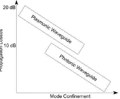
Figure 34: Relation between propagation losses in a plasmonic and in a photonic waveguides ... 51
Figure 35: Metal-Insulator-Semiconductor (MIS) waveguide. Both the semiconductor and the metal are semi-infinite ... 53
Figure 36: Analysis of the effective refractive index and the losses of the MIS waveguide [118] ... 54
Figure 37: Optical losses for Al and Cu in a MS plasmonic structure [123]... 57
Figure 38: Plot of the function G(η) and F(η) ... 64
Figure 39: Change in the energy bandgap of light and heavy holes due to biaxial tensile strain ... 65
Figure 40: Absorption spectrum of the material ... 66
Figure 41: Representation of the Airy functions A1 and B1 ... 68
Figure 42: Airy function Ai and its derivative A'i ... 71
Figure 43: Detail of the comparison of the model of the FKE (continuous line) and the measurements done in [46] (dotted line) ... 74
Figure 44: Flow chart of an integrated opto-electronic simulation ... 76
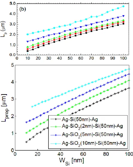
Figure 45: Effective refractive index of the supported mode in one branch of the MZI as a function of the refractive index of Si published in [57] on the left and reproduced by our integrated electro-optical modulator on the right ... 78
Figure 46: Effective propagation length of the supported mode in one branch of the MZI as a function of the refractive index of Si published in [57] in the left and reproduced by our integrated electro-optical modulator in the right ... 78
Figure 47: Effective refractive index of the supported mode in one branch of the MZI as a function of the width wSi of the core of the waveguide. It is taken from reference [57] on top and it is reproduced by our integrated electro-optical modulator on the bottom ... 79
Figure 48: Effective propagation length of the supported mode in one branch of the MZI as a function of the thickness of the SiO2 layer. It was published in [57] on top and reproduced by our integrated electro-optical modulator at the bottom ... 80
Figure 49: Effective refractive index of the supported mode in one branch of the MZI as a function of the width wSi of the core of the waveguide. It is taken from reference [57] on top and it is reproduced by our integrated electro-optical modulator on the bottom ... 81
Figure 50: Effective propagation lenght Lp of the supported mode in one branch of the MZI as a function of the width wSi of the core of the waveguide. It is taken from reference [57] on top and it is reproduced by our integrated electro-optical modulator on the bottom ... 82
Figure 51: Top view of photodetector butt-coupled to a standard Si rib waveguide. In this figure we have n-Si, p-Si and material 1 is Ge or SiGe... 83
Figure 52: Schematic of the structure to measure the FKE... 84
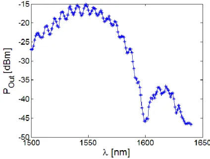
Figure 53: Measurement setup of the MMI ... 85
Figure 54: Measurement of Ptransmitted1 and Ptransmitted2 of the MMI using the structure of Figure 53 .... 86
Figure 55: POut versus wavelength when at PIN we inject 0 dBm. The parameters are defined in Figure 53 ... 86
Figure 56: I-V curve of the photodiode with the Ge core. It is represented the dark current Idark and the photocurrent for diferent wavelengths from 1510 nm to 1640 nm every 10 nm ... 87
Figure 57: I-V curve of the photodiode with the SiGe core. It is represented the dark current Idark and the photocurrent for diferent wavelengths from 1510 nm to 1640 nm every 10 nm ... 88
Ultra-compact plasmonic modulator for optical inteconnects Nicolás Abadía
x
Figure 58: Responsivity of the photodetector with Ge core versus the bias voltage V ... 89
Figure 59: Responsivity of the photodetector with SiGe core versus the bias voltage V ... 89
Figure 60: Scanning of the responsivity R of a SiGe photodetector ... 90
Figure 61: Measurement of the FKE done by other researchers at CEA-Leti (Leopold Virot) using photodetectors ... 91
Figure 62: Vertical PIN structure to induce a static electric field in the intrinsic core ... 98
Figure 63: Static electric field distribution induced in the intrinsic region of the vertical PIN of Figure 62 from 0 to 5 V in reverse bias ... 99
Figure 64: Modulator structure with a vertical PIN and a slot plasmonic waveguide around the intrinsic Ge ... 100
Figure 65: Normalized optical intensity distribution of the structure of Figure 64 ... 101
Figure 66: Static electric field distribution induced in the intrinsic region of the structure of Figure 64 from 0 to 5 V in reverse bias ... 102
Figure 67: Modulator structure with a vertical PIN and a slot plasmonic waveguide around the intrinsic Ge ... 103
Figure 68: Normalized optical intensity distribution of the optical field of the structure in Figure 67 ... 103
Figure 69: Static electric field distribution for the structure of Figure 67 ... 104
Figure 70: Horizontal PIN structure to induce a static electric field in the intrinsic core ... 105
Figure 71: Horizontal PIN structure with a plasmonic waveguide on top ... 105
Figure 72: Normalized optical intensity distribution in the horizontal PIN structure of Figure 71 ... 106
Figure 73: Static electric field distribution for a reverse bias for V=0 V and V=5 V in the structure of Figure 71 ... 106
Figure 74: Shifted horizontal PIN structure with a plasmonic waveguide on top ... 107
Figure 75: Structure of the slot plasmonic modulator ... 108
Figure 76: Capacitor-like structure for the FKE plasmonic modulator ... 109
Figure 77: Study of the influence of the patterned metal in the plasmonic modulator ... 111
Figure 78: Study of the influence of the patterned p-Ge layer in the plasmonic modulator ... 113
Figure 79: Optimized structure until Table 8 ... 114
Figure 80: Structure that is going to be optimized with respect to the parameters w and h of the NID Ge core ... 116
Figure 81: Capacitor-like structure with a MIS waveguide ... 120
Figure 82: Static electric field distribution in the middle of the device. In the cross-section x-x'. The applied bias voltage is around 10 V. It can be seen that the static electric field is confined in the Si3N4 barrier slot ... 122
Figure 83: Static electric field distribution in the middle of the device. In the cross-section x-x'. The applied bias voltage is around 3 V. It can be seen that the static electric field is desconfined in the Si3N4 barrier slot ... 123
Figure 84: Final structure of the FKE plasmonic modulator that is going to be optimized ... 124
Figure 85: Static electric field distribution for a driving voltage of (a) 0 V and (b) 3 V under the structure of Figure 48 ... 125
Figure 86: Optical field distribution of the plasmon TM mode supported by the MIS waveguide in the structure of Figure 84 ... 126
xi
Figure 88: Δαeff/αeff against the driving voltage V for the modulator of Figure 84. The width used is
w=150 nm ... 127 Figure 89: Extinction ratio of the device of Figure 84 as a function of the height of the Ge core h for different driving voltages V. The length is 30 µm ... 129 Figure 90: Propagation losses of the device of Figure 84 as a function of the height of the Ge core h for different driving voltages V. The length is 30 µm ... 130 Figure 91: Spectrum of the FoM |Δαeff|/αeff. The device is the optimized one. The maximums a and b
and the minimums 1 and 2 below the bandgap wavelength of the material are due to FKE oscilations ... 131 Figure 92: Absorption of the material αmat due to the FKE for a uniform static electric field in the
material of 0 V/cm and 105 V/cm ... 131
Figure 93: Equivalent electrical circuit of the plasmonic modulator ... 135 Figure 94: Structures to couple. Optimized plasmonic modulator (left) and Si rib waveguide (right) 141 Figure 95: Magnitude of the magnetic field H distribution of the fundamental TM mode of the
optimized plasmonic modulator ... 143 Figure 96: Effective refractive index neff of the plasmonic modulator of Figure 84. It is difficult to
calculate the effective index below 100 nm due to the amount of evanescent field ... 143 Figure 97: Effective absorption αeff of the plasmonic modulator of Figure 84. It is difficult to calculate
the effective index below 100 nm due to the amount of evanescent field ... 144 Figure 98: Silicon rib waveguide and its parameters ... 145 Figure 99: neff as a function of w for the Si rib waveguide. It is difficult to calculate the effective
refractive index below wSi=150 nm due to the deconfinement of the mode ... 146
Figure 100: Magnitude of the static electric field E and the magnetic field H in a Si rib waveguide with wSi=450 nm, hSi=255 nm and hSi-rib=100 nm... 147
Figure 101 : Magnitude of the static electric field E and the magnetic field H in a Si rib waveguide with wSi=800 nm, hSi=255 nm and hSi-rib=100 nm... 147
Figure 102: Representation of the butt-coupling structure between the Si rib waveguide and the optimized plasmonic modulator. The fixed parameters are hSi=255 nm and hrib-Si=100 nm ... 148
Figure 103: Simulation of the magnitude of the magnetic field in the plasmonic modulator for w=150 nm. In the left of the vertical withe line the Si rib waveguide is present while in the left of the vertical with line the plasmonic modulator is present. It is a side view of the structure of Figure 102 ... 149 Figure 104: Simulation of the magnitude of the magnetic field in the plasmonic modulator for w=250 nm. In the left of the vertical withe line the Si rib waveguide is present while in the left of the vertical with line the plasmonic modulator is present. It is a side view of the structure of Figure 102 ... 149 Figure 105: Simulation of the magnitude of the magnetic field in the plasmonic modulator for w=350 nm. In the left of the vertical withe line the Si rib waveguide is present while in the left of the vertical with line the plasmonic modulator is present. It is a side view of the structure of Figure 102 ... 150 Figure 106: Simulation of the magnitude of the magnetic field in the plasmonic modulator for w=450 nm. In the left of the vertical withe line the Si rib waveguide is present while in the left of the vertical with line the plasmonic modulator is present. It is a side view of the structure of Figure 102 ... 150 Figure 107: TTotal as a function of the propagation length x for different values of w. The selected
width of the Si rib waveguide is 450 nm. ... 151 Figure 108: Structure simulated in [143]. The red color is Si, the light blue is Al2O3 and the grey is Ag
Ultra-compact plasmonic modulator for optical inteconnects Nicolás Abadía
xii
Figure 109: Overlap integral between the modes supported by the plasmonic modulator and the
mode excited by the Si rib waveguide ... 153
Figure 110: TIn the mode inside the plasmonic modulator in the first 10 µm ... 155
Figure 111: TOther modes inside the plasmonic modulator in the first 10 µm ... 156
Figure 112: TScattered inside the plasmonic modulator in the first 10 µm ... 157
Figure 113: TTotal as a function of the propagation length x for different values of wSi ... 158
Figure 114: Overlap integral between the modes supported by the plasmonic modulator and the mode excited by the Si rib waveguide ... 158
Figure 115: TIn the mode inside the plasmonic modulator in the first 10 µm ... 159
Figure 116: Summary table of the main characteristics of the Ge taper summarized in Table 25 ... 160
Figure 117: Ge taper approach by inserting an intermediate Ge rib taper to match the effective refractive index of the Si rib waveguide and the optimized plasmonic modulator ... 161
Figure 118: Summary of the waveguides that are study to match the effective index between the standard Si rib waveguide and the optimized plasmonic modulator ... 162
Figure 119: All tapers comparison for a metal taper over Si, metal taper over Ge, Si rib waveguide taper and Ge rib waveguide taper ... 163
Figure 120: Germanium rib waveguide and its parameters ... 164
Figure 121: neff as a function of w for the Ge rib waveguide. It is difficult to calculate the effective refractive index below 150 nm due to the deconfinement of the mode ... 164
Figure 122: αeff as a function of w for the Ge rib waveguide. It is difficult to calculate the effective absorption coefficient below 150 nm due to the deconfinement of the mode ... 165
Figure 123: Scanning the parameter Ltaper to achieve the maximum of transmission into the fundamental TM mode of the optimized plasmonic modulator TIn the mode ... 166
Figure 124: TTotal as a function of the propagation length x for the Ge taper ... 167
Figure 125: TIn the mode inside the plasmonic modulator in the first 10 µm ... 168
Figure 126: Overlap integral between coupled electromagnetic field in the modulator and the mode excited by the Ge taper ... 169
Figure 127: TScattered inside the Ge taper (-1.5 µm<x<0 µm) and the optimized plasmonic modulator in the first 10 µm (0 µm<x<10 µm) ... 170
Figure 128: Overlap integral to measure the difference in the field profile between the two adjacent waveguides for the butt-coupling structure (left) and the Ge taper (right) ... 171
Figure 129: Summary Figure of the main characteristics of the Ge taper summarized in Table 26 ... 172
Figure 130: Magnitude of E and H of the fundamental plasmonic TM mode of the optimized modulator ... 173
Figure 131: Magnitude of E and H of the fundamental Si rib waveguide ... 173
Figure 132: Si-Ge taper into the Si rib waveguide to couple the optimized plasmonic modulator .... 174
Figure 133: Cross section of the Si-Ge taper of Figure 132 ... 175
Figure 134: neff as a function of wGe for the cross-section of the Si-Ge taper ... 175
Figure 135: αeff as a function of wGe for the cross-section of the Si-Ge taper ... 176
Figure 136: Study of the parameter wtaper in the total transmission through the modulator TTotal for different length of the length of the Si-Ge taper Ltaper ... 177
Figure 137: Study of the parameter wtaper in the overlap integral OI through the modulator TTotal for different length of the length of the Si-Ge taper Ltaper ... 178
Figure 138: Study of the parameter wtaper in the transmission in the mode TIn the mode through the modulatorfor different length of the length of the Si-Ge taper Ltaper ... 179
xiii
Figure 139: Summary table of the main characteristics of the Ge taper summarized in Table 27 ... 180
Figure 140: Diagram of the parameters meassured in Table 28 for the Ge and Si-Ge tapers and the butt-coupling scheme ... 182
Figure 141: Metal-dielectric interface to solve the propagation of SPP ... 192
Figure 142: Dispersion relation of SPP ... 196
Figure 143: First step of the layout fior the definition of the Si rib input/output waveguide and the grating ... 201
Figure 144: Definition of the input/output Si rib waveguide and the grating ... 201
Figure 145: Etching of a cavity in Si to place the core of the plasmonic modulator ... 201
Figure 146: Cavity filled with Ge and p-doped Ge ... 201
Figure 147: Definition and doping of the side contacts ... 202
Figure 148: Definition of the intrinsic Ge core of the modulator with side contacts ... 202
Figure 149: Deposition of the Si3N4 and the Cu layer ... 202
Figure 150: Final layout with the plasmonic modulator with side contacts and the input/output Si rib waveguide with the grating ... 203
Figure 151: Final layout of the plasmonic modulators. We can observe 24 sets of 16 modulators each ... 204
Figure 152: Detail of a set of 16 Ge plasmonic modulators ... 205
Figure 153: Empty waveguides to meassure the losses of the input/output Si rib waveguides ... 205
Figure 154: Layout of the fiber grating coupler designed to excite the fundamental TM mode at 1.647 µm of the Si rib waveguide ... 206
Figure 155: Example of a test spiral to meaasure the propagation losses of the TM photonic mode of the Si input/output rib waveguide ... 206
Ultra-compact plasmonic modulator for optical inteconnects Nicolás Abadía
xiv
List of Tables
Table 1: Comparative table of FKE photonic modulator... 24
Table 2: Comparative table of silicon photonics plasmonic modulators ... 33
Table 3: Comparative table of key silicon photonics modulators [29], [73] ... 38
Table 4: Efective refractive index of the metals for plasmonics ... 57
Table 5: Optical losses in a MIS waveguide for the different diffusion barriers that can be used [123] ... 58
Table 6: Summary of the plasmonic modulators structures studied until now ... 108
Table 7: Refractive index of the metals used to simulate the MS structure of Figure 39 ... 110
Table 8: Performance of the plasmonic modulator of Figure 39 for different metals ... 110
Table 9: Summary of the study of the patterned metal ... 111
Table 10: Summary of the study of the patterned metal ... 112
Table 11: Summary of the study of the influence of the buffer layer ... 112
Table 12: Summary of the study of the influence of the buffer layer ... 113
Table 13: Study of the doping of the Si layer for w=150 nm and h=400 nm. Used to check the results of Table 14 ... 115
Table 14: Study of the doping of the Si layer for w=250 nm and h=350 nm ... 115
Table 15: Optimization of the modulator of Figure 80 with respect to h for a w=150 nm ... 116
Table 16: Optimization of the modulator of Figure 80 with respect to h for a w=250 nm ... 116
Table 17: Summary of the performance of the device for the optimized modulator in Figure 43 ... 118
Table 18: Summary of the performance of the structure of Figure 81 with a slot thickness of 15 nm ... 122
Table 19: Optimization of the modulator of Figure 84 with respect to h for a w=150 nm ... 126
Table 20: Optimization of the modulator of Figure 84 with respect to h for a w=250 nm ... 126
Table 21: Summary of the performance of the device for the optimized modulator in Figure 84 ... 128
Table 22: Influence of the driving voltage V in the intrinsic capacitance of the modulator C ... 135
Table 23: Power consumption, minimum and maximum operational frequency (Fmin and Fmax) of the modulator ... 137
Table 24: Summary of the photonic FKE modulators and plasmonic modulators which reports the electrical power consumption ... 137
Table 25: Summary table of the main parameter of the butt-coupling structure ... 160
Table 26: Summary table of the main parameter of the Ge taper structure structure ... 172
Table 27: Summary table of the main parameter of the Si-Ge taper structure structure Figure 132. 180 Table 28: Summary table of the main characteristics of the coupling schemes studied. It is the butt-coupling, Ge taper and the Si-Ge taper ... 181
Ultra-compact plasmonic modulator for optical inteconnects Nicolás Abadía
1
1. Introduction
1.1
Context
In order to increase the operational frequency of the transistors, the semiconductor industry downscaled the size of the devices. There is an empirical law, called the Moore’s law [1], saying that for a constant fabrication cost, the number of transistors in the same surface of an electronic integrated circuit doubles every two years. Since the invention of the transistor [2], this empirical law seems to be true [3] but nowadays it is reaching its limit [4]. The number of transistors in a chip versus the year of invention is represented in Figure 1. The Moore’s law is satisfied since the first Intel 4004 [5] until the current Intel Core i7 [6]. This allows a reduction in the fabrication cost due to the mass production of the chips in the foundries.
There are different physical effects that happen in the downscaled transistors and that limit the performances of modern circuits [4]. The first one is that when the transistor is downscaled, the electrical wires within the circuit are also downscaled. This produces an increment in the resistance of such a wire. The increased resistance combined with the capacitance seen by the wire produces an increase of the RC delay [7] as well as the increase of heat dissipation due to the increment of the resistivity. A big delay causes a problem in the signal that propagates through a chip, for example, the clock signal on synchronous integrated circuits. Furthermore, the wires are closer and closer to each other when the electrical interconnect wires are downscaled. This produces an increment of the parasitic capacitance between wires which causes signal interference. This downgrades the
2
performances. It means, this capacitance plays a role in the crosstalk of the wires. As a consequence of this, there is interference in one wire due to the proximity of the adjacent ones.
Furthermore, the cited delay reduces the operational frequency of the chip because the computational delay is equal to the propagation delay through the chip. This problem is known as the interconnect bottleneck and it is a major problem in nowadays high performance computer integrated circuits.
Figure 1: Number of transistors versus the year of appearance. It follows the Moore's law [8]
Regarding the problem of increased resistivity due to the shrink of the interconnect wires it can be reduced using copper (Cu) instead of the well-established aluminum (Al). Cu has half of the resistivity of Al. Furthermore, the employment of low-κ dielectrics (E.g.: porous silica materials [9], SiOF, SiOC, polymers, etc.) is used to reduce the parasitic capacitances between wires.
The main problem of using Cu as a material for the intra-chip interconnects is that it is not a CMOS compatible material. Cu is a quick diffusion material into Si [10]. This fact can create a short circuit in the transistor between the source and the drain. Nevertheless, to avoid this, insulators barriers like SiO2, Si3N4 or HfO2 are used between the metal and the semiconductor. This invention allows the
Moore’s law to still remain a little bit more time [8]. Nevertheless, a long term solution needs to be addressed to circumvent the interconnect bottleneck.
One of the long term solutions to the problem of the interconnect bottleneck could be achieved by the use of silicon photonics [11], [12], [13], [14] whose main applications are to create optical links [15] to connect the different parts of the electronic integrated circuit. In this case the information is carried by photons instead of electrons; this leads to a reduction in the energy consumption as well as an increase in the operational frequency of the link [16]. For this, a set of silicon devices are needed. Namely: emitters, modulators, waveguides and detectors.
Another advantage of Si is that it is a widely available material and it has a low cost. It possesses a wide window with low optical losses (the main reduced losses are around 1.3 and 1.55 μm), a high optical damage threshold (the supported intensity is around 3 GW/cm2 and depending on the doping
Ultra-compact plasmonic modulator for optical inteconnects Nicolás Abadía
3
and the fabrication processes it can reach 5 GW/cm2) and good thermal conductivity. The good thermal
conductivity is important to well dissipate the heat from the integrated circuit.
Nowadays there are many optical communication systems [17], [18] that are commercially available and that are substituting electrical links in long distances (from 1 meter to many kilometers). This example of long-haul optical links overcomes the drawback of electrical ones. They can offer better bandwidth and fewer losses. Furthermore such long-haul optical interconnects are lighter with respect to the metal ones. Another advantage is that they are immune to electromagnetic noise.
One recent trend of silicon photonics is to carry the optical communications from the long-haul distances to intra-chip communications. It is believed that optical interconnects acting as a bus in a chip can overcome the limitations of metal interconnects and increase the performance.
Furthermore, another of the most important arguments of the technology is that the main used material is Si which is a well-known material in the semiconductor industry. Being CMOS compatible, it allows using the well-established foundries [19] and fabrication methods. This enables a massive fabrication of devices with the consecutive reduction in cost. One of the milestones of silicon photonics is to integrate in the same chip electronic and photonic devices.
1.2
Silicon Photonics
Probably Si is one of the most studied materials in the history. In this case silicon photonics [20] can take advantage of the well understood semiconductor Si. Furthermore, manufacturer machines in the foundries are well developing to fabricate small patterns of few nanometers. Taking into account that silicon photonics’ sizes are bigger than electronic features this allow a well precision in the fabrication process. Furthermore, the fact that the foundries are well established allows the mass production of photonic devices reducing the global cost of the product.
The use of the silicon-on-insulator (SOI) technology [21], [22] facilitates the integration with the electronic fabrication techniques and processes. It consists in a crystalline Si on silicon dioxide (SiO2).
A SOI waveguide is represented in Figure 2. This technology has the advantage that crystalline Si can be put over SiO2 using the SmartCut® technique [23]. With this method, the Si is crystalline. The main
use of this technology is to fabricate high contrast photonic waveguides. Such waveguides confine the light in small areas [24], [25], [26] due to the large refractive index difference between Si and SiO2. This
allows the fabrication of sharp bends and devices. Due to this fact the modal area can be as small as 400 nm for the width and 200-300 nm for the height.
4
Figure 2: Example of a strip waveguide with SOI technology
One of the main disadvantages of SOI waveguides, and in optics in general, is that they are limited in size reduction by the diffraction limit of light. The field of plasmonics tries to overcome the diffraction limit of light by using metals in the active region of the devices. This allows the design of smaller devices. It is expected that photonics devices reduces their dimensions enough to be integrated into an electronic integrated circuit. For doing this, the size of photonic devices and electronic ones are needed to be very close.
For setting an intra-chip optical interconnects, several elements are needed. Mainly, a source to produce the light within the integrated circuit, a modulator to encode the continuous wave (CW) light, a multiplexer to combine several wavelengths in one beam, waveguides to propagate the light from one point of the integrated circuit to another one, a demultiplexer to separate the wavelength and photodetectors to transform the information carried by the optical signal to the electrical one.
A schematic view of an optical link with its elements is presented in Figure 3. There are well-known several passive devices like waveguides but recently the main effort is taken to design sources [27], modulators [28] and photodetectors [29]. The first commercial silicon photonic-based optical data interconnect with integrated lasers is presented in [18] and [30].
Ultra-compact plasmonic modulator for optical inteconnects Nicolás Abadía
5
One important component to achieve an optical interconnect is the optical modulator [28] which converts the electrical signal that carries the information into an optical one. This device is the subject of this thesis.
It is worth to mention that Si is a centro-symmetric material making it difficult to design a modulator due to the absence of the Pockel’s effect. Furthermore, Si possesses an indirect band-gap. This is a main difficulty in the design of optical sources since the electron excitation from the valence band to the conduction one requires the presence of a phonon to conserve energy and momentum. The fact that Si is transparent at the wavelength of 1.55 μm does not allow the design of photodetectors at this wavelength. This is why other materials are being introduced in the field of silicon photonics. One of those examples is the use of Ge.
But even optical interconnects have its own challenges [31]. Some comparison between optical and electrical interconnects were found in [32].
1.3
Objective and Dissertation Outline
In the framework of this work, I want to develop a low power consumption modulator based on an electro-absorption effect. It will use the Franz-Keldysh effect (FKE) in germanium as the active principle of the deivce. To further reduce its power consumption we use a plasmonic structure as the optical waveguide to concentrate the light into the germanium core and reduce the size mismatch between photonic and electronic devices. The CMOS compatiblility is another main goal. Regarding the power consumption of the device we want that it is below 50 fJ/bit as stated in several roadmaps [4], [33] for future optical links.
Taking this brief summary of the device we propose, we introduce the outline of the chapters of this thesis in which we explain how we will design it, the rational of why electro-absorption modulator, why the FKE, why plasmonic structures, etc.
In the second chapter we introduce the basics and the state-of-the-art of silicon photonic modulators. For this, we do a small introduction to the device and its main characteristics. We explain the different effects that are used to perform the modulation and we do a state-of-the-art of the different photonic modulators that use the FKE. We also present all the silicon photonic plasmonic modulators. Since we are interested in low power consumption we explain at the end of the chapter the formulas used to calculate the energy consumption of modulators.
In the third chapter we introduce the field of plasmonics. We explain its advantages and disadvantages. We also discuss on CMOS compatibility and the metals that can be used. The metal-semiconductor (MS) and metal-insulator-metal-semiconductor (MIS) waveguides are also explained.
We also explain the rationale of using a plasmonics waveguide which we advance here. Since the appearance of integrated optics [34], optical devices tried to reduced their dimension and footprint in order to be integrated into an electronic chip. Nevertheless there is a miniaturization limit of photonic
6
devices due to the diffraction limit of light. Nowadays there is a dimensional mismatch between electrical and photonic integrated components. This mismatch difference hinders the integration of both electronic and photonics devices in the same wafer. This mismatch in size is due to the fact that photonic devices are limited in size by the diffraction limit of light. It is demonstrated that using metals the diffraction limit of light can be overcome and the dimensions of the devices can be reduced. This is why in the optical structure of our modulator we will use a plasmonic waveguide.
Regarding the power consumption, designing the modulator using metals to propagate light at the interface will allow a reduction of the dimensions of the device with respect to the photonic ones. The reduction of the device will also decrease the energy consumption of this. Furthermore, the reduction in the dimensions of the device will increase the interaction of the effects (FKE, carrier dispersion plasma effect, etc.) in Ge due to a bigger intensity of the electromagnetic fields within the material. Additionally, there is a trade-off between the losses of the propagating modes in a plasmonic waveguide and the spatial concentration of the electromagnetic field. It means, the smaller the spatial concentration of the electromagnetic field into a plasmonic waveguide, the bigger the propagation losses. Consequently, in our design, we want to have a small footprint but we also need to take care about the propagation losses of the modulator.
In the fourth chapter we explain the physics behind the FKE. We also derive mathematically the formulas to model the FKE. We present a simply generalized model and a more complete one. This model will be useful to calculate the main benchmarks of the device using the integrated electro-optic simulator that we introduce in the fifth chapter.
Regarding the low power consumption that we want to achieve we advance that, we want to design an electro-absorption modulator rather than an electro-refraction one. The main advantages of both electro-absorption over electro-refraction effects are that it allows the design of smaller devices (small footprint) and consequently it will have lower power consumption. This is why as a first glance we will discard electro-refraction over electro-absorption. The active principle of the modulator we want to design is the FKE. This effect is present in both silicon and germanium. Nevertheless the effect is stronger in germanium rather than in silicon. It is worth to mention that germanium can be integrated well in a silicon photonic fabrication process. Furthermore, the use of the FKE does not induce any limitation in the speed of the device since the FKE is an instantaneous effect (it is in the sub-picosecond regime [35]). The FKE will be analyzed and presented in the fourth chapter.
In chapter five we present the design of the plasmonic modulator which is the main objective of this thesis. We establish the benchmarks of the modulator that we want to achieve. We also explain the numerical tools that we are going to use to model the device and we present many structures to perform the modulation. We analyze the performance of each structure and we derive the main characteristics of the modulator mainly: the extinction ratio, the propagation losses, the energy consumption, etc.
For this we developed an opto-electronic integrated simulator. We use a commercial electrical simulator called ISE-dessis to calculate the static electric field distribution in the proposed structure of the modulator. With this information we apply a Franz-Keldysh effect model to calculate the change in the absorption of the material (in our case germanium). Knowing the absorption of the material we use a finite-difference method (FDM) mode solver to know how the effective losses of the mode are changed due to the mentioned Franz-Keldysh effect. With this tool we can obtain the main figure of
Ultra-compact plasmonic modulator for optical inteconnects Nicolás Abadía
7
merit of the modulator, it means, we can know the extinction ratio, the propagation losses, the bandwidth and the power consumption.
Using this tool we simulated many structures to act as a modulator and we selected the best performance. Knowing the good structure we optimized the device in order to increase the extinction ratio, decrease the propagation losses and reduce the power consumption.
The initial idea of the device is also discussed in the fifth chapter. We advance that we will use a plasmonic waveguide that can guide the light in the interface between the metal and a semiconductor. It is called a metal-semiconductor (MS) plasmonic waveguide. Placing germanium in the semiconductor part of the MS waveguide we will be able to exploit the FKE to produce the modulation of the plasmon. We want that a significant part of the plasmonic mode is in germanium. The germanium will be deposited in the core of the waveguide. We also want that the waveguide is connected to two electrodes in order to induce a static electric field in the germanium in order to change the absorption of the material and modulate the plasmon supported by the MS plasmonic waveguide. One electrode can be placed in the metal of the MS waveguide and the other below the semiconductor of the MS structure using a doped region. Inducing an electric field in the germanium will allow changing the optical absorption of the material. Since the plasmonic mode is also present in the germanium this will change the effective losses of such a mode, hence, producing the modulation of the plasmon. We will show that using a MS waveguide in the core of the modulator leads to high propagation losses of the plasmon. Instead of this we can use a traditional metal-insulator-semiconductor (MIS) waveguide. This waveguide, due to the use of an insulator layer, reduces the propagation losses of the plasmon.
Finally, in chapter six we design the coupling to the optimized structure designed in chapter five from a standard Si rib waveguide. The objective is to excite the proper mode of the modulator from the mentioned Si rib waveguide. For this we use 3D Finite-difference time-domain (FDTD) simulations. We used the commercial tool called Lumerical®. In this chapter we analyzed many different coupling structures (butt-coupling, tapers, etc.), we optimized them to increase the coupling efficiency into the modulator and finally we select the best one to place it in the device designed in chapter five.
Ultra-compact plasmonic modulator for optical inteconnects Nicolás Abadía
9
2 Silicon Optical Modulation
In this chapter we introduce the main characteristics of Si optical modulators. We explain the main effect for modulation in silicon photonics. We also do a state-of-the-art of photonic FKE modulators. Plasmonic modulators are also explained. Finally, we present the calculation of the electrical power consumption of these devices.
2.1
Introduction to Optical Modulators
Nowadays, the main application of silicon photonics is to try to substitute electrical interconnects by optical ones. The main objective is to increase the bandwidth and reduce the energy consumption. Furthermore, the main components of an optical interconnects are the light source, the modulator, the waveguide and the photodetector. One of the most important elements is the modulator. It can determine the bandwidth and it is the device which consumes a big portion of the power dissipated in the link. In this thesis we aim to design a compact and low-energy consumption modulator.
The modulator is a device which transforms an electrical signal that carries information into an optical one that also carries the same encoded information. In this case photons are used to transmit the information through a waveguide instead of electrons. For this, the modulator changes the phase, the intensity, the frequency or the polarization of a continues-wave (CW) light beam. The structure of an optical modulator is represented in Figure 4. In this example the information is encoded in the intensity of the light beam.
10
Figure 4: Schematic view of an optical modulator principle. In this case the information is encoded in the intensity of the light beam using an electrical signal
The main characteristics of an optical modulator are the insertion losses (IL), the extinction ratio (ER), the power consumption, the operational frequency or bandwidth (BW), the modulation voltage (VDD), the device footprint and the working spectrum. A good modulator has low insertion losses, a
high extinction ratio, consumes low energy and has a small footprint. We will specify the typical values and the objective for our modulator once we presented the state-of-the-art at the end of this chapter. The insertion losses are the optical losses from the input until the output of the device. They consist in both coupling and propagation losses through the device. Equation 1 quantifies this magnitude,
𝐼𝐿 = 10log (𝐼𝑚𝑎𝑥 𝐼0
) Equation 1
Where Imax is the maximum intensity of the encoded light beam at the output of the modulator
and I0 is the input intensity of the encoded light beam. It is represented in Figure 4.
The extinction ratio is related to the difference between the maximum intensity Imax and the
minimum intensity Imin of the encoded beam. It is represented in the following formula:
𝐸𝑅 = 10log (𝐼𝑚𝑎𝑥 𝐼𝑚𝑖𝑛
) Equation 2
Where Imax and Imin are the maximum and minimum intensities of the encoded light beam. It is
represented in Figure 4.
The power consumption is normally the electrical power consumption that the modulator employs to encode the light beam. It is given by the effort done by charging and discharging the electrical capacitance of the device. The electrical power consumption in energy per bit is given by,
∆𝐸𝑏𝑖𝑡=
1 4𝐶𝑉𝐷𝐷
2 Equation 3
Where ΔEbit is the energy per bit, C is the intrinsic capacitance of the device and VDD is the driving
Ultra-compact plasmonic modulator for optical inteconnects Nicolás Abadía
11
The optical power consumption is not normally given since it depends on the intensity I0 of the
input light beam. Nevertheless, the insertion loss is a good measure of the optical power consumption since it is proportional to it.
The operational frequency of the modulators measures the bandwidth of the modulator. It is a measure of the transmission velocity of the information.
The operational voltage is the voltage that the modulator requires in order to perform the modulation. The device footprint is given by the area that the modulator needs in the wafer. Finally, the working spectrum is the wavelength range within which the modulator can work.
In the following section we will describe the different effects that can be used in Si to modulate a CW beam of light from an electrical signal.
2.2
Optical Modulation Effects
Depending on the physical effect that the modulator uses to encode the information it can be classified as electro-absorption or electro-refraction device. In the case of electro-absorption devices the effect used changes the optical absorption coefficient of the material and consequently modulates the intensity of the optical light beam. On the other hand, electro-refraction devices change the refractive index of the material. In this case the phase of the optical CW beam is modified. The use of structures like ring resonators (RR) or Mach-Zenhder interferometers (MZI) can transform the change in phase into the change in the optical intensity.
In the following sections, we explain the different effects used in silicon photonics to perform the modulation. They are divided on electro-refraction effects and electro-absorption effects.
2.2.1 Electro-Refraction Effects
In this section we explain the electro-refraction effect used in silicon photonics. Those effects change the refractive index of the material in order to change the phase of the optical propagating signal. The main effects are the thermo-optic effect, the Pockels and Kerr effects and the plasma dispersion effect.
12
2.2.1.1 Thermo-Optic Effect
In the thermo-optic effect the application of heat to the material is used to change the refractive index of it. Neither an electric field nor the injections of carriers are used in this effect. The thermo-optic coefficient of Si [36] is:
𝑑𝑛 𝑑𝑇=
1.86x10⁻⁴
𝐾
Equation 4
A refractive index change of the order of 10-3 happens when a temperature variation of 10°C is
applied to Si. There are some problems like controlling the changes of temperature uniformly [37] in all the volume of the material.
Another issue is that the operational frequency of the device is not big since heating and cooling down the material is a slow process. The operational frequency of thermo-optic devices is around 100 kHz. Some modulators [36] and switches have been proposed [38].
2.2.1.2 Pockels and Kerr Effect
When a static electric field is applied in a medium it may change its refractive index of the material. This effect is called the Pockels [39] effect when the change is proportional to the static electric field. If the change is quadratic then it is called the Kerr effect or the Quadratic Electro-Optic effect (QEO effect) [40]. The change in the refractive index as a function of the applied static electric field is given by,
∆ (1 𝑛𝑟2
) = rE + s𝐸2+ ⋯ Equation 5
In the previous equation nr represents the refractive index of the material, E is the electric field, r
is the electro-optic Pockels coefficient and s is the electro-optic Kerr coefficient. The Pockels and the Kerr effects change the polarizability of the material; consequently, the change in the refractive index depends on the polarization of the electric field with respect to the optical axes of the material.
Pockels effect is present in crystals without inversion symmetry. Some materials which exhibit good Pockels effect are: indium phosphide (InP), gallium arsenide (GaAs) or lithium niobate (LiNbO3).
On the other hand, the Kerr effect is present in any material.
As explained before, the Pockels effect is not present in Si because it is a centro-symmetric material. Recent research showed that straining the Si, the centro-symmetry is broken and consequently a Pockels effect can be measured [41]. A modulator is proposed in [42] using this technique. Normally, to break the symmetry, a silicon nitride (Si3N4) layer is deposited over the Si. This
Ultra-compact plasmonic modulator for optical inteconnects Nicolás Abadía
13
Regarding the Kerr effect, it can be measured in Si but it is a weak effect [43]. The breakdown static electric field of Si must be exceeded in order to obtain a significant change in the refractive index of the material. The breakdown static electric field of Si is around 3x10⁵ V/cm. The range of the change
in the refractive index at the wavelength of 1.3 µm is around Δn=10-3-10-4 [43]. Where, Δn is the change
in the refractive index of the material. In conclusion, it is not a good effect to design an optical modulator.
2.2.1.3 Plasma Dispersion Effect
When the concentration of carriers is changed into a semiconductor it modifies both the refractive index and the optical losses of the material due to the Kramers–Kronig relations. This is called plasma dispersion effect or free carrier dispersion effect. When the number of carriers is increased in a semiconductor like Si, the refractive index decreases while the optical losses of the material are increased. Inversely, if the concentration of carriers decreases we have the opposite effect.
The theoretical change in the refractive index and in the optical losses against the concentration of electrons and holes is giving by the following theoretical equations:
∆n = −𝑒 2𝜆 0 2 8𝜋2𝑐2𝜀 0𝑛 (𝑁𝑒 𝑚𝑐𝑒∗ + 𝑁ℎ 𝑚𝑐ℎ∗ ) Equation 6 Δα = 𝑒 3𝜆 0 2 4𝜋2𝑐3𝜀 0𝑛 ( 𝑁𝑒 𝜇𝑒(𝑚𝑐𝑒∗ )2 + 𝑁ℎ 𝜇ℎ(𝑚𝑐ℎ∗ )2 ) Equation 7
Where Δn is the change in the refractive index of the medium, Δα is the change in the optical absorption of the medium, e is the electric charge of the electron, λ0 is the wavelength of the incoming
light, c is the velocity of the light in vacuum, ε0 is the electrical permittivity of vacuum, n is the refractive
index of the medium, Ne and Nh are the concentrations of electrons and holes in the medium, µe and
µh are the mobility of electrons and holes and m*ce and m*ch are the reduced effective mass of electrons
and holes.
There is also an experimental study of the change of the refractive index and the optical absorption of the material in [43]. The authors studied those changes for many different carrier concentrations at the wavelengths 1.3 µm and 1.55 µm. The results are in good agreement with the theoretical formulas given by Equation 6 and Equation 7. The derived empirical formulas at λ0=1.55 µm are:
∆𝑛 = ∆𝑛𝑒+ ∆𝑛ℎ
= −[6.2𝑥10−22∆𝑁𝑒
+ 6.0𝑥10−18(∆𝑁 ℎ)0.8]
14 ∆𝛼 = ∆𝛼𝑒+ ∆𝛼ℎ = 6.0𝑥10−18∆𝑁𝑒 + 4.0𝑥10−18∆𝑁 ℎ Equation 9
Where Δne and Δnh are the changes in the refractive index caused by free electrons and free holes
that are present in the material. Δαe and Δαh are the changes in the optical absorption caused by free
electrons and free holes that are present in the medium. It is expressed in cm-1. From those equations
we can see that for a carrier concentration of 5x1017 cm-3 we can obtain a change of Δn in the order of
10-3 for 1.3 µm.
From Equation 8 and Equation 9 we can see that holes are more efficient than electrons in changing the refractive index of the material Δn for a free carrier concentration ΔN<1019 cm-3. This effect can be
achieved by carrier injection, depletion or accumulation [28]. Normally this effect is used to change the phase of light into a waveguide. To change the amplitude of the incoming light beam structures like MZI and RR are used.
2.2.2 Electro-absorption Effects
2.2.2.1 The Franz-Keldysh Effect
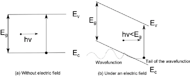
The Franz-Keldysh effect (FKE) [44], [45] is the change of the optical material absorption for wavelengths close to the direct energy bandgap (E.g.: Si and Ge) when an external static electric field is applied to the bulk material. The energy diagrams used to explain the FKE are represented in Figure 5. Under no applied static electric field into the material, the conduction and valence band are like in Figure 5 (a). Then a photon of energy bigger than Eg (energy bandgap of the material) can excite an
electron from the valence band to the conduction band. It is represented in the Figure 5 (a). Nevertheless, when an electric field is applied into the material both the valence and the conduction bands are tilted like in Figure 5 (b). In this case the wave-function of the electrons in the valence band can penetrate into the forbidden band by tunneling. Due to this tunneling, a photon with less energy than the bandgap of the material Eg can excite an electron from the valence band to the conduction
one producing the absorption of light. It is represented in Figure 5 (b). This increases the optical absorption of the material just below the energy bandgap Eg. This is known as the FKE. Due to the
Kramers–Kronig relation when the absorption of the material is changed then the refractive index of it is also modified. So, the FKE produce electro-absorption and electro-refraction.
Ultra-compact plasmonic modulator for optical inteconnects Nicolás Abadía
15
Figure 5: Energy diagram of the FKE. In (a) there is not a static electric field while in (b) a static electric field is applied
The FKE is both present in Si and Ge. It is bigger in Ge than in Si due to the sharper band-edge in Ge. Near the band-edge of Si there is absorption due to phonons that softs the band-edge of Si. The FKE was measured experimentally in Si in [43]. They measured the optical absorption of the material due to the FKE and using the Kramers–Kronig relation they calculate the electro-refraction. Note that this electro-refraction is cause by the FKE and not due to plasma dispersion effects.
As a conclusion, the FKE in Ge is stronger than in Si for the reasons explained in the previous paragraph. Several photonic modulators were proposed using the FKE in Ge. In this thesis we will use the FKE to produce the modulation of a plasmon. This effect will be detailed in chapter four.
The FKE also depends on the strain that the Ge has. The first observation of FKE in Ge over Si is reported in [46]. The structure studied is a PIN junction made of Ge over a Si wafer. When the Ge is deposited over the Si there is a biaxial stress caused by the difference in the thermal expansion coefficients between Ge and Si during deposition of Ge over the Si at a high temperature (750 °C) the Ge experiences a compressive strain. Nevertheless, when it is cooled down it presents a biaxial tensile strain. There is a thermal process that allows the creation of a tensile strain around 0.20 % [47]. This produces the narrowing of the direct bandgap of Ge. Furthermore, due to the strain there is a degeneration of the heavy and light holes in the valence band. Without strain the valence band of heavy and light holes is degenerated. The tensile strain also reduces the energy difference between the valence and conduction bands. This shifts the band-edge (and consequently the FKE) to longer wavelengths. The energy band of Ge is represented in the following Figure 6,
16
Figure 6: Energy band structure of Ge and the influence of biaxial tensile strain [29]
In the left energy diagram of Figure 6 we see the direct gap in the Γ point. The indirect band-gap occurs at the point labeled L. Furthermore, the indirect band-band-gap L is less than the direct band-band-gap Γ. It is worth noting that in the valence band the light hole band and the heavy hole band are non-degenerated in the strained case.
Furthermore, in this strained case the direct band-gap Γ is now smaller than the indirect band-gap L for enough biaxial tensile strain. It will be interesting to know how the gap energy of the direct band-gap Eg(Γ) and the indirect one Eg(L) changes with the biaxial tensile strain of the material. It is
represented in Figure 7,
Figure 7: Influence of the biaxial tensile strain in the direct and indirect band-gaps in Ge [29]
From Figure 7 we see the influence of the biaxial tensile strain on the direct energy gaps Eg(Γ) and
the indirect energy gap Eg(L). We will model the FKE in a Ge which is strain 0.2%. Consequently, the
energy gap of the direct band-gap Eg(Γ) will be larger than the energy gap of the indirect one Eg(L). As
we explained using Figure 6 we see that the direct energy gap Eg(Γ) is decreasing as the biaxial tensile
strain increases. Using the values of Figure 6 we can predict the FKE for different strains using the FKE model that we will describe in chapter five.
![Figure 6: Energy band structure of Ge and the influence of biaxial tensile strain [29]](https://thumb-eu.123doks.com/thumbv2/123doknet/15039278.691208/32.892.206.862.108.344/figure-energy-band-structure-influence-biaxial-tensile-strain.webp)

![Figure 20: Structure of the arm of the CMOS compatible elector-absorption modulator and top view [65]](https://thumb-eu.123doks.com/thumbv2/123doknet/15039278.691208/45.892.324.721.460.734/figure-structure-cmos-compatible-elector-absorption-modulator-view.webp)
![Figure 27: Example of slot photonic waveguides to further confine the light in a smaller cross section [85]](https://thumb-eu.123doks.com/thumbv2/123doknet/15039278.691208/62.892.344.700.104.387/figure-example-photonic-waveguides-confine-light-smaller-section.webp)
![Figure 37: Optical losses for Al and Cu in a MS plasmonic structure [123]](https://thumb-eu.123doks.com/thumbv2/123doknet/15039278.691208/73.892.327.722.652.971/figure-optical-losses-for-al-and-plasmonic-structure.webp)