Design and Simulation for the Fabrication of
Integrated Semiconductor Optical Logic Gates
by
Aleksandra Markina
S.B., Massachusetts Institute of Technology (1999)
S.M., Massachusetts Institute of Technology (2001)
Submitted to the
Department of Electrical Engineering and Computer Science
in partial fulfillment of the requirements for the degree of
Doctor of Philosophy in Electrical Engineering
at the
MASSACHUSETTS INSTITUTE OF TECHNOLOGY
September 2005
©Massachusetts Institute of Technology 2005. All rights reserved.
Author ...
Department of Electrical Engineering and Computer Science
September 19, 2005
Certified by ...
Leslie A. Kolodziejski
Professor of Electrical Engineering
Thesis Supervisor
Accepted by ...
Arthur C. Smith
Chair, Department Committee on Graduate Students
Design and Simulation for the Fabrication of
Integrated Semiconductor Optical Logic Gates
by
Aleksandra Markina
Submitted to the
Department of Electrical Engineering and Computer Science
in partial fulfillment of the requirements for the degree of
Doctor of Philosophy in Electrical Engineering
ABSTRACT
Development of ultrafast all-optical logic requires accurate and efficient modeling of optical components and interfaces. In this research, we present an all-optical logic unit cell with complete Boolean functionality as a representative circuit for modeling and optimization of monolithically integrated components. Proposed optical logic unit cell is based on an integrated balanced Mach-Zehnder interferometer (MZI) with semiconductor optical amplifiers (SOAs) in each arm and includes straight ridge waveguides, ridge waveguide bends, and multimode interference (MMI) devices.
We use beam propagation method (BPM) to model, design and optimize dilute ridge waveguides, MMIs, and asymmetric twin waveguide (ATG) adiabatic taper couplers. We assess device robustness with respect to variations in fabrication, including lateral pattern transfer and etching. Bending losses in curved waveguides are evaluated using complex-frequency leaky mode computations with perfectly matched layer (PML) boundary conditions. Finite difference time domain (FDTD) method with PML is utilized in calculating reflections produced by abrupt interfaces, including a tip of an adiabatic taper coupler. We demonstrate that evaluating reflections based on local effective indices on two sides of the junction offers a simple, accurate, and time-efficient alternative to FDTD. We show a strategy for development of SOAs for linear
amplification and phase shifting using the same layered semiconductor structure. Our model of optical pulse propagation in SOA is based on rate equations for carrier density and photon density and using a wavelength-dependent parametric model for gain. We demonstrate a tradeoff between injection current density and device length for both linear and non-linear SOAs.
Thesis Supervisor: Professor Leslie A. Kolodziejski Title: Professor of Electrical Engineering
ACKNOWLEDGEMENTS
I am grateful to my research advisor Professor Leslie Ann Kolodziejski for an opportunity to work on research projects in her lab. Her patient support and guidance extended far beyond the area of molecular beam epitaxy and semiconductor optical devices. In addition to her virtues as a supervisor, I would like to thank her for bringing together a group of most friendly, gracious, and helpful individuals I had a pleasure to work with. I hope at some point in my future professional life to be part of the team of colleagues half as wonderful.
This work would not be a success without the tireless support of Dr. Gale Petrich. His willingness to sacrifice his time and to share his vast expertise with graduate students does much to brighten many of their days.
I am indebted to Professor Rajeev Ram for his guidance and invaluable insights, especially crucial in my study of semiconductor optical amplifiers. I would also like to thank Professor Erich Ippen and Dr. Scott Hamilton for valuable discussions of all-optical signal processing.
The following people made significant contributions to various parts of my
research project. Professor Vinod Menon helped me to get started with the simulations of taper couplers. Miloš Popović shared his script for calculating modes of leaky dielectric structures, making calculation of losses in bent waveguides possible. Dmitry Vasilyev was of immense help with his Matlab wizardry. Fuwan Gan performed FDTD
calculations of reflections from abrupt semiconductor interfaces.
It was my honor and my pleasure to work alongside graduate students of Integrated Devices and Materials Group. Solomon Assefa was a fellow physics undergrad. During our graduate studies he shared with me his contagious energy and optimism. Reginald Bryant was my neighbor both in the office and, for almost a year, in the dorm as a fellow GRT. I was grateful to Reggie for all those times we spent working quietly on our projects as well as those time when we distracted ourselves with a
conversation. I truly enjoyed his sense of humor. Eric Mattson joined us briefly in our office, and his fellowship was very welcome as well. Sheila Tandon inspired me with her focus and hard work. Thanks and wishes of good luck go to Ryan Williams, my main collaborator on the optical logic unit cell project.
Many thanks are due to my family for their patience, support, encouragement, and help. Everything I ever achieved I owe to my parents, Anatoliy and Vera. It is also hard to overestimate the support I always receive from my extended family as well as my husband’s: Michael’s parents, Boris and Yelena, and all of our grandparents and relatives. My grandfather Leonid should be especially noted for taking full care of my family in the final week of my graduate work. Michael and I enjoy the loyalty and help of many wonderful friends who are like family to us here in Boston, none more than Kathryn Myer who adopted me as her sister.
I am indebted to my husband Michael for his unyielding support of my graduate studies as well as his exquisite skill with Microsoft Office tools which he generously shared with me in the preparation of this document and my defense presentation. Michael accompanied me on my entire MIT journey. A little less than a year ago we were joined by our daughter, Xenia. I was delighted to have her constantly by my side in the final chapter of my MIT saga.
TABLE OF CONTENTS
1 Introduction...14
1.1 Motivation...14
1.2 Master example—optical logic unit cell ...17
1.2.1 Materials ... 18
1.2.2 Fabrication ... 19
1.2.3 Device performance ... 20
1.3 Overview...21
2 Passive Devices ...29
2.1 Passive Ridge Waveguides ...29
2.1.1 Beam Propagation Method ... 30
2.1.1.1 Including polarization effects in the BPM ... 34
2.1.1.2 Mode solving with BPM... 35
2.1.1.3 RSoft BeamPROP... 37
2.1.2 Main examples—Optimization of dilute ridge waveguides ... 38
2.1.2.1 Simulations of Bulk WGs ... 39
2.1.2.2 Selection of layered materials... 40
2.1.2.3 Robustness of dilute ridge waveguides with respect to fabrication variations... 42
2.1.3 Passive ridge waveguides—Conclusions... 43
2.2 Passive waveguide bends...44
2.2.1 Attempts to assess bending losses with BPM ... 45
2.2.2 Bending loss calculation by finite-difference method with cylindrical PML ... 47
2.2.3 Bending losses in curved dilute waveguides—Results... 49
2.2.4 Optimization of coupling junctions ... 50
2.2.5 Ridge waveguide bends—conclusions ... 51
2.3 Multimode Interference Devices...52
2.3.1 Principle of operation... 52
2.3.2 Guided Mode Propagation Analysis ... 53
2.3.2.1 Propagation constants ... 53
2.3.2.2 Guided-mode propagation analysis... 54
2.3.2.3 General interference... 55
2.3.2.4 1x2 MMIs realized by symmetric interference... 57
2.3.2.5 2x2 MMIs realized by paired interference... 57
2.3.3 Main examples: MMIs... 59
2.3.3.1 1x2 MMI ... 60
2.3.3.2 2x2 MMI ... 64
2.3.3.3 Combiners ... 66
2.3.3.4 Tolerance to underetching of trenches... 68
2.3.4 Multimode interference devices—Conclusions... 73
3 Interfaces Between Passive and Active Devices ...79
3.1 Review of monolithic integration techniques ...81
3.1.1 Butt coupling... 81
3.1.2 Quantum well disordering... 82
3.1.3 Asymmetric Twin Waveguides... 85
3.2 Main BPM examples—Optimization of Asymmetric Twin Waveguides ...89
3.2.2 BPM simulations of adiabatic taper couplers ... 95
3.2.2.1 Simulation of ATG without tapers... 99
3.2.2.2 Selection of taper length ... 99
3.2.2.3 Selection of layer geometry ... 101
3.2.2.4 Robustness of ATG taper couplers with respect to fabrication variations ... 105
3.2.2.5 Triple ridges ... 109
3.3 Finite Difference Time Domain Method ...111
3.3.1 Perfectly Matched Layer boundary conditions... 115
3.3.2 FDTD simulations of abrupt interfaces... 119
3.4 Overall loss in passive waveguides and couplers ...124
4 Semiconductor Optical Amplifier ...132
4.1 Physical principles behind semiconductor optical amplifier operation ...133
4.2 Applications of semiconductor optical amplifiers in photonic integrated circuits...137
4.3 Semiconductor Optical Amplifiers for Linear Amplification...138
4.3.1 Comparison of semiconductor optical amplifier and Erbium-doped fiber amplifier... 138
4.3.2 Materials with long carrier lifetime ... 140
4.3.3 Gain-clamped semiconductor optical amplifiers (GC-SOA)... 141
4.3.4 Non-uniform current injection ... 142
4.4 Semiconductor Optical Amplifiers for All-Optical Signal Processing...142
4.4.1 All-optical signal processing schemes ... 142
4.4.3 Use of keying to overcome pattern dependence ... 147
4.5 Modeling...150
4.5.1 Rate equations... 151
4.5.2 Parameterized gain model... 152
4.5.3 Wave propagation ... 154
4.5.4 Nonlinear phase ... 155
4.5.5 Simplifying assumptions... 157
4.6 Major examples...158
4.6.1 Amplified Spontaneous Emission... 159
4.6.2 Linear amplifier ... 162
4.6.2.1 Gain saturation... 162
4.6.2.2 Small signal gain... 163
4.6.3 Output saturation power... 166
4.6.4 Device Optimization ... 169
4.6.4.1 SOA for linear amplification ... 169
4.6.4.2 SOA as a phase shift element... 172
4.6.5 Conclusions... 174
5 Summary and Directions for Future Work...181
5.1 Summary ...181
5.1.1 Passive devices... 181
5.1.2 Interfaces between passive and active devices ... 183
5.1.3 Semiconductor Optical Amplifiers ... 184
5.2 Future directions ...186
Appendix B Design Files for RSoft Simulations ...190 Appendix C MATLAB Programs ...205
TABLE OF FIGURES
Figure 1-1. Optical logic unit cell... 18 Figure 2-1. Bulk Ridge Waveguide. ... 39 Figure 2-2. Dependence of mode effective index on bulk index in bulk ridge waveguides
of cross section 4 mm x 1.05 μm. ... 39 Figure 2-3. Dependence of mode effective index on ridge width in bulk ridge
waveguides, bulk index 3.22 and height of 1.05 μm. ... 40 Figure 2-4. Dilute ridge waveguide design... 41 Figure 2-5. Dependence of mode effective index on ridge width in dilute ridge
waveguides... 42 Figure 2-6. Curved ridge waveguide. ... 44 Figure 2-7. Losses in curved ridge waveguide. ... 50 Figure 2-8. Fundamental mode of a) straight ridge waveguide; b) curved ridge
waveguides (R=500 μm)... 51 Figure 2-9. Offset optimization between a straight and a curved waveguide... 51 Figure 2-10. Highest-order mode of the 12 μm wide multimode section... 61 Figure 2-11. Output of 1x2 MMI splitter: a) ideal, b) computed for the described design.
... 62 Figure 2-12. Operation of 1x2 MMI splitter... 63 Figure 2-13 Optical power in one of 1x2 MMI outputs as a function of multimode section length... 63 Figure 2-14. Operation of 2x2 MMI as a 3 dB splitter. ... 66
Figure 2-15. Optical power in 2x2 MMI outputs as a function of multimode section
length... 66
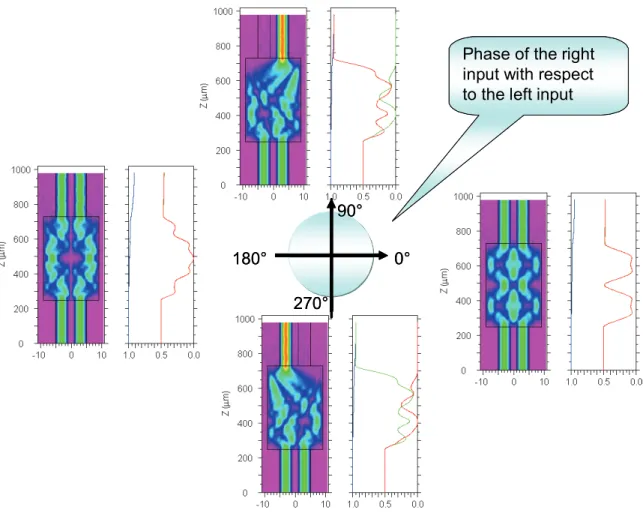
Figure 2-16. 2x1 MMI combiner a) inputs in phase; b) inputs 180° out of phase... 67
Figure 2-17. Operation of 2x2 MMI with different relative phases between the two inputs... 68
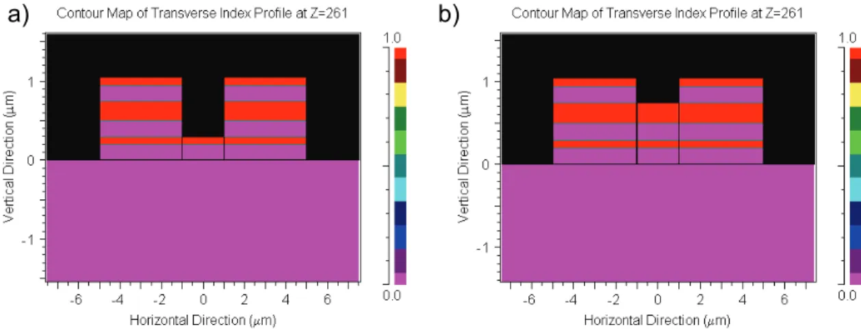
Figure 2-18. Index profiles of output waveguides with underetched trenches: a) moderately underetched; b) severely underetched... 69
Figure 2-19. Optical power oscillations in the output waveguides with a severely underetched trench... 71
Figure 2-20. Modes of the properly etched structure... 71
Figure 2-21. Modes of severely underetched structure... 72
Figure 3-1. Asymmetric twin-waveguides structure [119]. ... 89
Figure 3-2. Lateral layout of tapered ATG structure. ... 90
Figure 3-3. Cross-section of ATG structure. ... 91
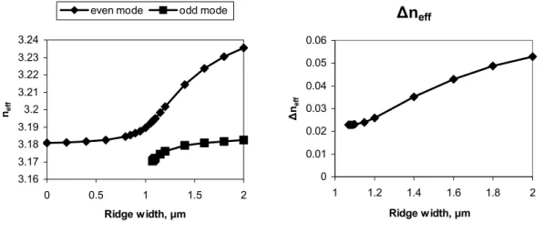
Figure 3-4. Effective indices of confined modes of ATG structure as a function of taper width. ... 93
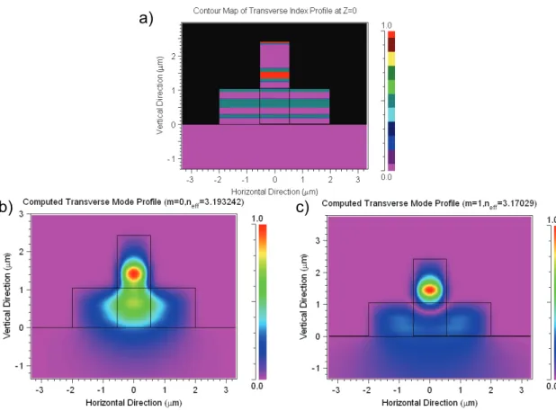
Figure 3-5. ATG structure begins to support the second mode at ridge width of 1.07 μm. a) Index profile, b) Fundamental mode, c) First-order mode. ... 94
Figure 3-6. Fundamental modes of a) passive waveguide and b) ATG (with respective index profiles). ... 95
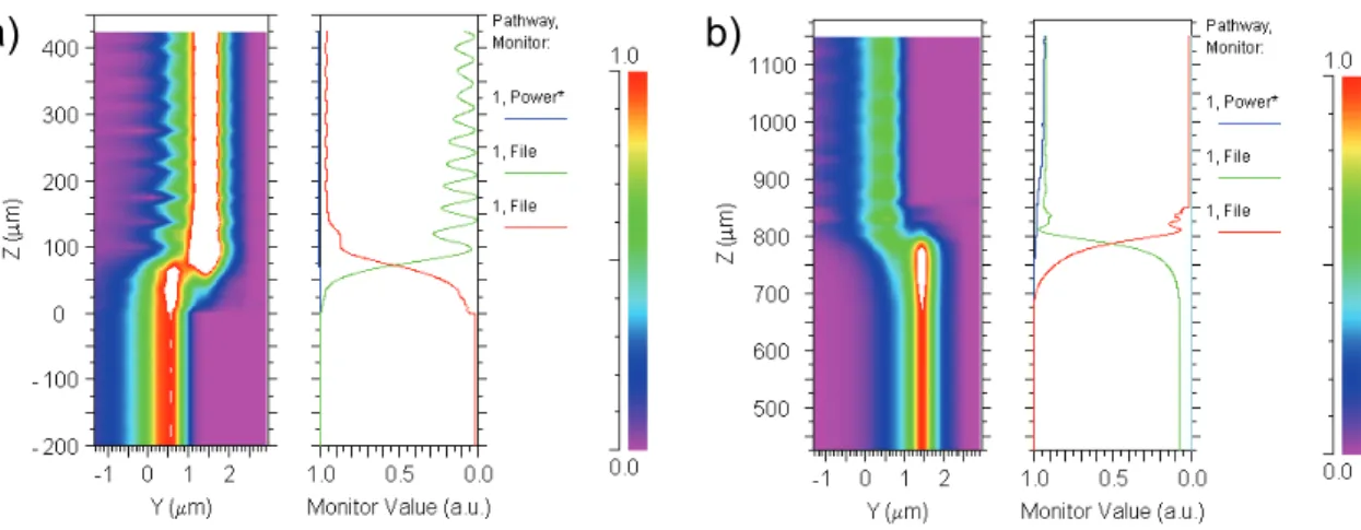
Figure 3-7. Transfer of energy from passive guide to ATG. ... 96
Figure 3-9. Examples of BPM simulations of optical power transfer a) from passive guide
to ATG, b) from ATG to passive guide. ... 98
Figure 3-10. Highest-order mode of the double ridge. ... 98
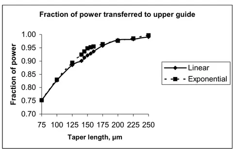
Figure 3-11. Coupling efficiency of linear and exponential tapers as a function of taper length... 100
Figure 3-12. Cross-section of ATG structure with variable spacer and cap layers. ... 102
Figure 3-13. Coupling efficiency as a function of cap layer thickness... 102
Figure 3-14. Coupling efficiency as a function of spacer layer thickness. ... 103
Figure 3-15. Fundamental mode of ATG for cap thickness of a) zero, b) 0.7 μm. ... 104
Figure 3-16. Cross-sectional view of fundamental mode of ATG for cap thickness of a) zero, b) 0.7 μm. ... 105
Figure 3-17. Coupling efficiency as a function of reduction in upper ridge width. ... 106
Figure 3-18. Coupling efficiency as a function of the missing length of the taper... 106
Figure 3-19. Coupling efficiency as a function of the initial width of the taper... 107
Figure 3-20. Rotational misalignment of the upper ridge (taper length = 175 μm, SOA width = 2 μm, cap width = 2 μm). ... 108
Figure 3-21. Coupling efficiency as a function of misalignement angle... 109
Figure 3-22. Fundamental mode of ATG for several variations of ridge geometry. ... 110
Figure 3-23. Upper-right part of a computational domain surrounded by the PML layer [139]... 117
Figure 3-24. Simplification of taper tip for FDTD modeling. ... 121
Figure 3-25. Optical power propagation by FDTD from passive waveguide to ATG. .. 122
Figure 4-1. Carrier and gain dynamics [145]... 134
Figure 4-2. Erbium-Doped fiber amplifier [151]... 139
Figure 4-3. Quantum Dot SOA [172] (g is the ground state; ex is the excited state)... 145
Figure 4-4. Keying schemes [179]... 149
Figure 4-5. Typical input and output of the numeric simulator... 155
Figure 4-6. ASE power as a function of injection current density, LSOA=0.4 mm. ... 160
Figure 4-7. ASE power as a function of injection current density, LSOA=1.5 mm. ... 161
Figure 4-8. ASE power as a function of SOA length, J=8x10³ A/cm2. ... 162
Figure 4-9. Gain saturation, LSOA=0.4 mm, J=8x10³ A/cm2... 163
Figure 4-10. Small signal gain as a function of wavelength, LSOA=0.4 mm, J=8x10³ A/cm2. ... 164
Figure 4-11. Small Signal Gain as a function of injection current density, LSOA=0.4 mm. ... 165
Figure 4-12. Small Signal Gain as a function of SOA length, J=8x10³ A/cm2. ... 165
Figure 4-13. Output saturation power and small signal gain as a function of confinement factor, LSOA=0.4 mm, J=8x10³ A/cm2... 167
Figure 4-14. Output saturation power and small signal gain as a function of SOA length, J=8x10³ A/cm2. ... 168
Figure 4-15. Output saturation power and small signal gain as a function of injection current density, LSOA=0.4 mm. ... 169
Figure 4-16. Gain as a function of SOA length and injection current density... 171
Figure 4-18. Nonlinear phase as a function of SOA length and injection current density. ... 173 Figure 4-19. Nonlinear phase as a function of bias current. ... 173 Figure 5-1. Cascading multiple unit cells to perform operation f(A,B,C,D) [49]. ... 187
1 Introduction
1.1 Motivation
Currently, network services impose bottlenecks on fiber optic communications. While network management complexity increases with the number of wavelengths fibers carry, most signal processing operations, such as switching and routing, are still
performed electronically after opto-electronic (OE) conversion [1, 2]. An average internet session takes 16 hops, with OE-EO conversions for electronic switching at each node. Development of ultrafast all-optical logic would make it possible to avoid multiple conversions and to distribute low-level network functionality in the optical core. High-level slow processing would then be pushed to network edges. Desired functionality of all-optical signal processing includes routing, synchronization, header processing, and cascadability [2-4]. Developing a family of optical logic with complete Boolean functionality—an optical equivalent of Transistor-Transistor Logic (TTL)—is an important step in this direction.
A fast non-linear element is required to implement optical signal processing functions. Semiconductor Optical Amplifier (SOA) represents an especially attractive choice. SOA is integrable, relatively compact, and boasts good thermal stability and high non-linearity [5]. To utilize fast nonlinear response of SOAs and mask their slow
recovery, SOAs can be inserted into interferometer arms [6]. Symmetric Mach-Zehnder configurations with identical SOAs placed in each arm of Mach-Zehnder interferometer (MZI) are especially effective. When nonlinear refractive index change is induced in the two SOAs with an appropriate delay, cross-phase modulation is utilized to change the amplitude of the interferometer output [4]. MZIs with SOAs are robust and highly integrable, and thus represent a valuable platform for realization of optical signal processing functions.
A wide variety of optical components is required in order to perform every function currently carried out by electronic circuits. These include optical clocks [7, 8], polarization splitters [9-12], polarization rotators [13-15], TE/TM mode converters [16, 17], straight and bent waveguides [18-20], Semiconductor Optical Amplifiers [21-23], various filters (for example, Bragg filters [24], side coupled resonator filters [25-29], tunable Fabry-Perot filters [30, 31]), isolators [32-34], time delay components [35-39], phase shifters [40-43], multimode interference couplers [44, 45], and fiber-to-chip
couplers [46-48]. As evidenced by an abundance of literature describing design, building and operation of the above components, significant progress has been achieved in
creating discrete elements for future optical networks. Despite these considerable research efforts, many existing devices are bulky and barely compatible. Therefore, effective integration of optical components on a chip represents a bottleneck in all-optical circuit development.
To address the bottleneck issue we need to monolithically integrate optical logic gates. Such gates need to be easy to fabricate, robust and reliable in operation.
efficient modeling tools. In contrast to the electronic devices and circuits field, optical design field lacks standard, universal design and simulation tools.
The goal of this research is to develop and test a strategy for design of the integrated optical circuit components. This task requires mastery of a set of
semiconductor device modeling tools. The challenge is to optimize the performance of each component while all the components are monolithically integrated on a
semiconductor chip. The reach the goal of monolithic integration, it is crucial to develop a simulation environment for the selection of device design and performance
optimization. Numerical modeling needs to address all relevant material properties, fabrication techniques and their tolerances, device performance and optimization based on tradeoffs between device parameters and performance priorities.
Device modeling serves a range of invaluable functions. First of all, it allows a designer to monitor internal variables in order to gain better understanding of device physics. Second, modeling yields an estimate of device performance without the need to build the device. Since fabrication and testing of novel semiconductor devices typically requires significant resources of time, labor, materials and equipment, accurate modeling results in significant savings. In addition, simulations provide a way to optimize device performance by varying device parameters, testing parameter range, and finding optimal operating conditions for required device functionality. Numerical modeling also helps to identify tradeoffs between device specifications and operating parameters. Once such tradeoffs are recognized, intelligent choices can be made based on the design priorities. Finally, modeling allows for robustness analysis of the design with respect to possible variations in fabrication results.
1.2 Master example—optical logic unit cell
An all-optical circuit based on Mach-Zehnder interferometer (MZI) geometry capable of performing all operations of Boolean algebra (AND, NAND, XOR) is an optical analog of Transistor-Transistor Logic (TTL). It is useful in a wide variety of applications for all-optical data processing. Such unit logic cell can be built on an optical bench from an assortment of discrete semiconductor components connected with optical fiber [49]. In order to make the circuit practical for real-world optical networks, it needs to be integrated on a semiconductor chip. An integrated implementation of the optical circuit will make the unit logic cell compact and cascadable: several unit cells can be arranged to perform more involved optical data processing.
In this work, an all-optical logic unit cell serves as a representative circuit for modeling and optimization of monolithically integrated components. Proposed optical logic unit cell is based on an integrated balanced Mach-Zehnder interferometer with an SOA in each arm (Figure 1-1). The basic version of this photonic integrated circuit consists of straight ridge waveguides, ridge waveguide bends, multimode interference (MMI) power splitters and combiners, and semiconductor optical amplifiers (SOAs). The basic implementation does not address the issues of timing, reflections, and separating multiple co-propagating wavelengths.
A
B
A
Δφ 1
SOA 1
SOA2 Δφ 2
Δτ
Δφ 1
SOA 1
SOA2 Δφ 2
Δτ
MMI
MMI
MMI
MMI
Figure 1-1. Optical logic unit cell.
1.2.1 Materials
Material system of choice for this project is (In,Ga)(As,P) grown on InP
substrates. This material system has a number of advantages compared to other photonic materials such as GaAs, silicon, silica, and polymers. InGaAsP/InP has high refractive index which makes compact, high index contrast structures possible. Our chosen material system also possesses high electrical conductivity and medium thermal
conductivity. Most importantly, InGaAsP/InP system offers significantly higher gain at 1.55 μm wavelength than does any other material system listed above.
In1-xGaxAsyP1-y lattice matched to InP offers a bandgap range from 0.73eV
(InGaAs) to 1.35eV (InP) which makes it highly compatible with all-optical fiber networks. Quaternary material of a desired bandgap can be obtained by choosing the appropriate ratios of group III and group V elements [50]. It is necessary to identify materials with desirable properties for both passive and active devices. Passive
waveguides has to be transparent to 1.55 μm light, exhibit low loss and minimal
polarization sensitivity. Active device layers need to provide sufficient gain at 1.55 μm. A suitable quaternary material for an active core is In0.56Ga0.44As0.93P0.07 because it is
lattice matched to InP and has a bandgap corresponding to 1.57 μm.
1.2.2 Fabrication
A vertical semiconductor structure is realized by a crystal growth. An epitaxial growth provides excellent control over composition and thickness of semiconductor layers. Molecular beam epitaxy (MBE) is characterized by direct physical transport of material components from effusion cells to a heated substrate wafer. The process takes place under high vacuum conditions. These conditions allow the use of various
diagnostic tools and in-situ processes including thermal or ion beam cleaning, Auger electron spectroscopy, mass spectroscopy, x-ray photoelectron spectroscopy, and radiation high energy electron diffraction [50, 51]. Epitaxially-grown heterostructures form the base for the circuit design.
Lateral patterning is performed by optical lithography followed by dry and wet etching steps. Fabrication processes required for building integrated optical logic unit cell are similar to conventional III-V processing sequences. Dielectric deposition is performed by Plasma Enhanced Chemical Vapor Deposition (PECVD) or sputtering. Gold-containing metal contacts are typically deposited by electron beam evaporation. Etching techniques include reactive ion etching and wet etches [49]. Exploring fabrication tolerances is a crucial part of device modeling.
1.2.3 Device performance
Elements of the all-optical logic unit cell are chosen as representative components in our study of semiconductor device modeling for PIC design. Appropriate modeling techniques need to be chosen for each optical component. Numerical methods have to addresses crucial device phenomena, parameters, and requirements.
Passive devices have to be transparent to 1.55 μm light. Other desirable
characteristics of passive components include low loss and low polarization sensitivity. The cross-section of the passive waveguide should be sufficiently large for easy coupling to an optical fiber. Waveguide bends should be as compact as possible. Multimode interference couplers are required to operate as balanced, efficient splitters and combiners.
Minimizing reflectivity is the most important design guideline for interfaces between passive and active components of the photonic integrated circuits. Low reflectivity is especially important for integrated SOAs: a reflection coefficient below 10-4 is needed in order to operate an SOA as a single-pass device without creating a laser
cavity. In addition, robust, efficient couplers need to be designed to guide optical energy between passive and active components.
Two types of semiconductor optical amplifiers are employed in the optical logic unit cell. The first type is a linear amplifier. In this application, a linear SOA needs to provide only a moderate level of amplification with a highly linear behavior at the lowest injection current density possible. The second SOA type is a non-linear phase shift element. The non-linear SOA has to supply a π phase shift for a modest SOA length and
injection current density. Both types of SOAs have to perform their functions for signals several picoseconds in lengths with energies on the order of hundreds of femtoseconds.
1.3 Overview
The following three chapters share a similar logical structure. Each chapter concentrates on one class of devices with specific applications in photonic integrated circuits. We choose appropriate numerical techniques that address crucial device characteristics. We explain the mathematical basis for modeling, including simplifying assumptions and limitations of each numerical method. Next we apply the described simulation techniques to design examples chosen among optical logic unit cell components. We discuss simulation results and their implications for device
optimization, identify tradeoffs between device parameters, and in some cases examine design robustness with respect to likely imperfections in device fabrication.
In Chapter 2, we discuss passive devices: bulk and dilute ridge waveguides, curved ridge waveguides, and multimode interference (MMI) devices. We use semi-vectorial Beam Propagation Method implemented by RSoft Corporation to find confined optical modes of the waveguide structures and to study light propagation in the
multimode waveguides. We demonstrate design process for the passive devices starting with a choice of passive material layers for straight ridge waveguides. This vertical structure is shared by all passive devices and therefore represents a starting point for an MMI design. We briefly present the theory of MMI devices that guides and informs our computer-aided design process for MMIs. Special attention is paid to likely
imperfections in ridge waveguide and MMI fabrication and to the effect of these imperfections on simulated device performance. In addition, we survey numerical
techniques for estimating losses in curved ridge waveguides and show calculations of bending losses using finite-difference method with cylindrical perfectly matched layer (PML) boundary conditions. The discussion of curved ridge waveguides also includes an optimization process for coupling junctions between waveguides of different curvature.
In Chapter 3, we address the problem of modeling interfaces between passive and active optical components. We begin with a review of main monolithic integration techniques: butt coupling, Quantum Well Disordering (QWD), and Asymmetric Twin Waveguides (ATG). Since ATG approach it employed in the design of an all-optical unit cell, we discuss the history and evolution of ATG method in some detail. We also
address the physical nature of coupling through tapered waveguides. We demonstrate the optimization process for ATG tapers using BPM software and access robustness of taper couplers with respect to fabrication variations. Next, we introduce the finite difference time domain technique (FDTD) with perfectly matched layer (PML) boundary conditions for calculation of reflections from abrupt interfaces. We use FDTD with PML to
determine reflections from butt-coupling interfaces as well as from the ATG taper tip. We also show that reflection coefficient can be accurately estimated based on local effective indices before and after the junction. This alternative method is considerably less time-consuming and demands far fewer computational resources.
In Chapter 4, we review physical processes behind semiconductor optical
amplifier (SOA) operation. We discuss the origins of slow and fast dynamic response in an SOA and their consequences for SOA use in linear and non-linear applications. In order to highlight desirable characteristics of a linear optical amplifier, we compare SOA with an Erbium-Doped Fiber Amplifier (EDFA). Next, we mention several techniques
for obtaining improved linear SOA performance, including the use of materials with a long carrier lifetime, non-uniform current injection and gain clamping. In the following sections, we switch to the discussion of SOA use in all-optical signal processing schemes. We detail two general approaches to overcoming pattern dependence in all-optical
circuits employing SOAs: the use of Quantum Dot SOAs and utilization of special signal encoding methods. In the later part of Chapter 4, we present a model of light propagation in SOA based on rate equations for carrier and photon density in the device. The
simulation method employs the wavelength-dependent parametric gain model and allows us to estimate gain and phase experienced by an optical pulse passing through an SOA. We use the described simulation technique to implement optimization of a linear and a non-linear SOA. We demonstrate a process for selecting SOA length and injection current density for a linear SOA which produces a desired gain and a non-linear SOA which produces a specified phase shift. Both cases reveal a tradeoff between SOA length and bias current density. As we will show, this tradeoff is important for optimization of SOA performance.
Chapter 5 contains a summary of results presented in this work. The chapter concludes with a brief discussion of future directions in semiconductor device modeling and in optical logic until cell design.
1. D. Cotter, et al., Nonlinear Optics for High-Speed Digital Information
Processing. Science, 1999. 286: p. 1523.
2. R.J. Manning, et al. Recent advances in all-optical signal processing using
semiconductor optical amplifiers. 1999.
3. K. Tajima. Ultrafast all-optical signal processing with symmetric Mach-Zehnder type all-optical switches. 2001.
4. S. Nakamura, Y. Ueno, and K. Tajima. Ultrahigh-speed optical signal processing
with symmetric-Mach-Zehnder-type all-optical switches. 2002.
5. B. Dagens, et al. SOA-based devices for all-optical signal processing. 2003.
6. K. Uchiyama and T. Morioka. All-optical signal processing for 160
Gbit/s/channel OTDM/WDM systems. 2001.
7. B. Sartorius, et al. Self-pulsation at more than 20 GHz in InGaAsP/InP DFB
lasers in Semiconductor Laser Conference 1992.
8. S. Fischer and M.G. Dulk, E.; Vogt, W.; Gini, E.; Melchior, H.; Hunziker, W.; Nesset, D.; Ellis, A.D. , Optical 3R regenerator for 40 Gbit/s networks
Electronics Letters 1999. 35(11): p. 2047 -2049.
9. F. Ghirardi and J.C. Brandon, M.; Bruno, A.; Menigaux, L.; Carenco, A. ,
Polarization splitter based on modal birefringence in InP/InGaAsP optical waveguides IEEE Photonics Technology Letters, 1993. 5(9): p. 1047 –1049.
10. F.J. Mustieles, E. Ballesteros, and F. Hernandez-Gil, Multimodal analysis method
for the design of passive TE/TM converters in integrated waveguides IEEE
Photonics Technology Letters, 1993. 5(7): p. 809 -811.
11. J.J.G.M. van der Tol, et al., Mode evolution type polarization splitter on
InGaAsP/InP. IEEE Photonics Technology Letters, 1993. 5(12): p. 1412 -1414.
12. L.B. Soldano and A.I.S. de Vreede, M.K.; Verbeek, B.H.; Metaal, E.G.; Green, F.H. , Mach-Zehnder interferometer polarization splitter in InGaAsP/InP IEEE Photonics Technology Letters, 1994. 6(3): p. 402 –405.
13. S. S. A. Obayya, B.M.A.R., K. T. V. Grattan and H. A. El-Mikati Beam
Propagation Modeling of Polarization Rotation in Deeply Etched Semiconductor Bent Waveguides IEEE Photonics Technology Letters, 2001. 13(7): p. 681-683.
14. H. Heidrich, et al., Passive mode converter with a periodically tilted InP/GaInAsP
rib waveguide IEEE Photonics Technology Letters, 1992. 4(1): p. 34-36.
15. C. M. Weinert and H. Heidrich, Vectorial simulation of passive TE/TM mode
converter devices on InP IEEE Photonics Technology Letters, 1993. 5(3): p. 324
-326.
16. M. Schlak, et al., Tunable TE/TM-mode converter on (001)-InP-Substrate. IEEE Photonics Technology Letters, 1991. 3(1): p. 15-16.
17. P. Albrecht, et al. Polarization converter and splitter for a coherent receiver
optical network on InP in IEE Colloquium on Polarisation Effects in Optical Switching and Routing Systems. 1990.
18. M. Rajarajan, et al., Characterization of low-loss waveguide bends with
offset-optimization for compact photonic integrated circuits. IEE Proceedings on
Optoelectronics 2000. 147(6): p. 382-388.
19. P. Bienstman, et al., Calculation of Bending losses in dielectric waveguides using
eigenmode expansion an perfectly matched layers. IEEE Photonics Technology
Letters, 2002. 14(2): p. 164-166.
20. J. Singh, et al., Single-mode low-loss buried optical waveguide bends in
GaInAsP/InP fabricated by dry etching. Electronics Letters, 1989. 25(14): p. 899
-900.
21. S. Kitamura, et al., Angled facet S-bend Semiconductor optical Amplifiers for
high-gain and large extinction ratio. IEEE Photonic Technology Letters 1999.
11(7): p. 788-790.
22. A. Lestra and J.-Y. Emery, Monolithic Integration of Spot-Size Converters with
1.3 um lasers and 1.55um polarization insensitive semiconductor optical
amplifiers. IEEE J Selected Topics in Quantum Electronics, 1997. 3(7): p.
1429-1440.
23. K. Djordjev, S.J.C., W.J. Choi, S.J. Choi, I. Kim and P. Dapkus, Two-segment
spectrally inhomogeneous traveling wave semiconductor optical amplifiers applied to spectral equalization. IEEE Photonic Technology Letters, 2002. 14(5):
p. 603-605.
24. M. J. Khan, et al. Integrated Bragg grating structures. in Advanced
Applications/Ultralong Haul DWDM Transmission and Networking/WDM Components, 2001. Digest of the LEOS Summer Topical Meetings 2001.
25. M.K. Chin, et al., GaAs microcavity channel-dropping filter based on a
race-track resonator IEEE Photonics Technology Letters, 1999. 11(12): p. 1620 –
1622.
26. C. Manolatou, et al., Coupling of modes analysis of resonant channel add-drop
filters Quantum Electronics, IEEE Journal of, 1999. 35(9): p. 1322 –1331.
27. S. Fan, et al., Channel Drop Tunneling through Localized States. Physics Review Letters, 1998. 80: p. 960–963.
28. P.P.Absil, et al., Vertically coupled microring resonators using polymer wafer
bonding. IEEE Photonics Technology Letters 2001. 13(1): p. 49 -51.
29. B.E. Little, et al., Microring resonator arrays for VLSI photonics. IEEE Photonics Technology Letters 2000. 12(3): p. 323 -325.
30. N. Chitica, et al., Monolithic InP-biased tunable filter with 10-nm bandwidth for
optical data interconnects in the 1550-nm band IEEE Photonics Technology
Letters, 1999. 11(5): p. 584 –586.
31. H.K. Tsang, et al., Etched cavity InGaAsP-InP waveguide Fabry-Perot filter
tunable by current injection. Journal of Lightwave Technology, 1999. 17(10): p.
1890 –1895.
32. H. Yokoi, et al., Feasibility of integrated optical isolator with semiconductor
guiding layer fabricated by wafer direct bonding IEE Proceedings on
Optoelectronics, 1999. 146(2): p. 105 -110.
33. H. Yokoi and T. Mizumoto, Integration of terraced laser diode and optical
isolator by wafer direct bonding Conference on Lasers and Electro-Optics
Europe, 2000: p. 1.
34. M. Takenaka and Y. Nakano. Proposal of a novel semiconductor optical
waveguide isolator in Conference on Indium Phosphide and Related Materials.
1999.
35. W. Ng, et al., High-precision detector-switched monolithic GaAs time-delay
network for the optical control of phased arrays IEEE Photonics Technology
36. S. Yegnanarayanan, et al., Compact silicon-based integrated optic time delays IEEE Photonics Technology Letters, 1997. 9(5): p. 634 –635.
37. E.J. Murphy, et al., Guided-wave optical time delay network IEEE Photonics Technology Letters 1996. 8(4): p. 545 –547.
38. N.F. Hartman and L.E. Corey. A new time delay concept using integrated optics
techniques in Antennas and Propagation Society International Symposium. 1991.
39. N.F. Hartman, et al. Integrated optic time delay network for phased array
antennas in IEEE National Radar Conference. 1991.
40. B.H.P. Dorren, et al., A chopped quantum-well polarization-independent
interferometric switch at 1.53 um IEEE Journal of Quantum Electronics, 2000.
36(3): p. 317 -324.
41. J.E. Zucker, et al., Electro-optic modulation in a chopped quantum-well electron
transfer structure Electronics Letters, 1994. 30(6): p. 518 -520.
42. B.H.P. Dorren, et al., Low-crosstalk penalty MZI space switch with a 0.64-mm
phase shifter using quantum-well electrorefraction IEEE Photonics Technology
Letters 2001. 13(1): p. 37 -39.
43. B.H.P. Dorren, et al., Low-crosstalk penalty MZI space switch with a 0.64-mm
phase shifter using quantum-well electrorefraction IEEE Photonics Technology
Letters, 2001. 13(1): p. 37 -39.
44. J. Leuthold, et al., Multimode interference couplers for the conversion and
combining of zero- and first-order modes. Journal of Lightwave Technology,
1998. 16(7): p. 1228 –1239.
45. P.A. Besse, et al., New 2x2 and 1x3 multimode interference couplers with free
selection of power splitting ratios. Journal of Lightwave Technology, 1996.
14(10): p. 2286 -2293.
46. Soo-Jin Park, et al., A novel method for fabrication of a PLC platform for hybrid
integration of an optical module by passive alignment. IEEE Photonics
Technology Letters, 2002. 14(4): p. 486-488.
47. D. Taillaert, et al., An Out-of-Plane Grating Coupler for Efficient Butt-Coupling
Between Compact Planar Waveguides and Single-Mode Fibers Journal of
48. K. Kato and Y. Tohmori, PLC hybrid integration technology and its application
to photonic components IEEE Journal on Selected Topics in Quantum
Electronics, 2000. 6(1): p. 4-13.
49. A. Markina, G. S. Petrich, and L. A. Kolodziejski, Towards Integrated Photonic
Circuits. 2002, Research Laboratory of Electronics, Massachusetts Institute of
Technology.
50. E.H.C. Parker, The Technology and Physics of Molecular Beam Epitaxy. 1985:
Plenum Press.
51. A. Katz, Indium Phosphide and Related Material: Processing, Technology, and Devices. 1992: Artech House, Inc.
2 Passive Devices
2.1 Passive Ridge Waveguides
Design of ridge waveguides requires fast and accurate calculations of waveguide modes. Rigorous approach calls for solving a full set of Maxwell equations for 3D geometry. Closed-form solutions are not available; therefore numeric methods must be used. There exist a number of methods. Semi-analytical methods include Marcatili’s method [52, 53], Effective Index method [54-57], Fourier transform techniques [58], the Spectral Index [59-61], and the Free Space Radiation Mode methods [62-64]. While these methods are efficient and fast, their use is limited to particular geometries.
Numerical methods such as Finite Difference [65-67], Finite Element [68, 69], and Finite Difference Beam Propagation Method [70-72] are accurate, robust, and applicable to a wide range of problems [73, 74]. We chose Beam Propagation Method (BPM) for modeling of ridge waveguides because BPM is conceptually straightforward, efficient, and uses modest computational resources to yield sufficiently accurate results. It serves our simulation goals well because in most cases the computational effort is directly proportional to the number of grid points used in the numerical simulation. The beam
propagation method (BPM) is the most widely used technique for modeling integrated photonics devices [75].
The BPM is a technique for approximating the exact wave equation for monochromatic waves and solving the resulting equations numerically by finite difference method. The basic approach requires assumptions of a scalar field and paraxiality. However, to insure that the switch performance is the same for TE and TM polarized light we need to use enhanced BPM. To address the issue, among available options we turn to semi-vectorial version of BPM.
The BPM technique can be applied to complex geometries without having to develop specialized versions of the method. Another advantage of BPM is that it automatically includes the effects of both guided and radiating fields as well as mode coupling and conversion. The BPM approach is extensible, that is, it allows for the inclusion of effects such as polarization and nonlinearities by extensions of the basic method.
Polarization effects can be included in the BPM by using the vector wave equation rather than the scalar Helmholtz equation. Semi-vectorial approximation is achieved by decoupling the transverse components of the electric field. As a result of this approximation, the problem is considerably simplified while retaining the most
significant polarization effects. In this work, the semi-vectorial BPM is used.
2.1.1 Beam Propagation Method
Beam Propagation Method (BPM) is a recursive procedure for calculating electro-magnetic field distribution in a plane from the field distribution in a preceding parallel plane [75, 76]. Basic approach is formulated under the restrictions of paraxiality and a
scalar field. Paraxiality restricts propagation to a narrow range of angles. The scalar field assumption means that polarization effects are neglected. The scalar electric field
can be written as E(x,y,z,t)=φ(x,y,z)e−jωt. The geometry of the device is completely
defined by the refractive index distribution n(x,y,z).
The wave equation can be stated as Helmholtz equation for monochromatic waves: 0 ) , , ( 2 2 2 2 2 2 2 = + ∂ ∂ + ∂ ∂ + ∂ ∂ φ φ φ φ z y x k z y x (Eq. 2-1)
where the spatially-dependent wavenumber is given by k(x,y,z)=k0n(x,y,z), with λ
π / 2
0 =
k being the wavenumber in free space.
For most guided-wave problems, the phase variation due to propagation along the guiding axis represents the fastest variation in the field φ. Since paraxial approximation allows us to assume that the axis is predominantly along the z direction, it is possible to factor this rapid variation out by introducing a slowly varying field u and restating φ as
z k i e z y x u z y x, , ) ( , , ) ( = φ , (Eq. 2-2)
where k is a constant that represents the average phase variation of the field φ. This constant is referred to as the reference wavenumber and can be expressed in terms of
reference refractive index, n : k =k0n. Substituting Eq. 2-2 into Eq. 2-1 yields the equation equivalent to the exact Helmholtz for the slowly varying field:
0 ) ( 2 2 2 2 2 2 2 2 2 = − + ∂ ∂ + ∂ ∂ + ∂ ∂ + ∂ ∂ u k k y u x u z u k i z u . (Eq. 2-3)
Invoking paraxial approximation one more time, it is assumed that the variation of
u with z is sufficiently slow that the first term in Eq. 2-3 is negligible compared to the second, that is,
z u k z u ∂ ∂ << ∂ ∂ 2 2 2
. Eq. 2-3 is now reduced to
⎟⎟
⎠
⎞
⎜⎜
⎝
⎛
−
+
∂
∂
+
∂
∂
=
∂
∂
u
k
k
y
u
x
u
k
i
z
u
)
(
2
2 2 2 2 2 2 . (Eq. 2-4)The above equation forms the basis of three-dimensional BPM and completely
determines the evolution of the field for z>0 given an input field u(x,y,z=0). The last simplification reduces the problem from a second order boundary value problem to a first order initial value problem. While the former requires iteration or eigenvalue analysis, the latter can be solved by simple “integration” of Eq. 2-4 along the direction of propagation z.
Early versions of BPM employed split-step Fourier method for “integrating” parabolic partial differential equation Eq. 2-4 forward in z. Later an implicit finite-difference approach (FD-BPM) based on Crank-Nicholson scheme has become standard [75]. Compared to Fourier transform-based methods, FD-BPM achieves comparable accuracy using a larger step size. Another advantage is a lower computational time per step [73]. In FD-BPM, the field in the transverse (xy) plane is represented at discrete points. Numerical equations are used to determine the field at the next discrete plane along the propagation direction (z) from the discretized field at the previous z plane. First, we will illustrate this approach for a scalar field in 2D (xz).
Let’s assume that grid points and planes are equally spaced by x and z
n i
u . In the Crank-Nicholson method Eq. 2-4 is written for the midplane between the plane of the known field n and the next plane, n+1:
(
)
(
)
2 , 2 1 2 2 2 1 2 2 1 n i n i n i n i n i k x z k u u x k i z u u + ⎟⎟ ⎠ ⎞ ⎜⎜ ⎝ ⎛ − + Δ = Δ − + + + δ , (Eq. 2-5)where δ2 is the second order difference operator, ( 2 ) 1 1 2 i i i i u u u u = + + − − δ , and 2 / 2 1 z z
zn+ ≡ n +Δ . When the above equation is rearranged into the form of a tridiagonal matrix equation for the unknown field n+1
i
u in terms of known quantities, it results in
i n i i n i i n i iu bu cu d a + + + = + + + −11 1 11 . (Eq. 2-6)
Expressions for the coefficients ai, bi, ci, and di are derived in [77]. Since Eq. 2-6
is tridiagonal, it can be solved in order O(N) operations, where N is the number of grid points in x.
Appropriate choice of boundary conditions is crucial for accurate BPM calculations because a poor choice can cause an artificial reflection of light from the boundary of the computational domain. Early research made use of absorbing boundary conditions (ABC) where an artificial absorbing material is placed near the edge of the domain. The ABC approach has several serious disadvantages. First of all, the absorber parameters are problem-dependent. Optimizing them for a particular problem requires significant effort and care. Moreover, in many cases, artificial reflections persist because the interface between the computational space and the artificial absorber is also partially reflective. Transparent boundary condition (TBC) was introduced to address the above problems. In the TBC approach the outgoing field is allowed to pass the domain boundary as an outgoing plane wave. The TBC approach is more versatile, robust, and requires less computer memory than the ABC. It works well for problems with narrow
propagation angles. Since paraxial condition holds for most of the structures considered in this work, the TBC approach is employed wherever BPM is used [73, 75].
The direct extension of the Crank-Nicholson approach to 3D results in a system of
equations that is not tridiagonal and therefore requires ( 2 2)
y
x N
N
O ⋅ operations to solve directly. A numerical approach called the alternating direction implicit (ADI) method allows the 3D problem to be solved with optimal O(Nx⋅Ny) efficiency. The ADI approach is employed by the BPM program used for this work [75].
2.1.1.1 Including polarization effects in the BPM
Polarization effects can be included by using the vector wave equation instead of the scalar Helmholtz equation. The equations for the vector electric field E can be formulated in terms of the transverse components of the field, Ex and Ey. This approach
results in a set of coupled equations for the slowly varying fields ux and uy:
y xy x xx x A u A u z u + = ∂ ∂ (Eq. 2-7) y yy x yx y A u A u z u + = ∂ ∂ (Eq. 2-8)
Complex differential operators Aij are given by
( )
⎭ ⎬ ⎫ ⎩ ⎨ ⎧ − + ∂ ∂ + ⎥⎦ ⎤ ⎢⎣ ⎡ ∂ ∂ ∂ ∂ = x x x x xx u k k u y u n x n x k i u A 1 ( ) 2 2 2 2 2 2 2 (Eq. 2-9)( )
⎭ ⎬ ⎫ ⎩ ⎨ ⎧ − + ⎥ ⎦ ⎤ ⎢ ⎣ ⎡ ∂ ∂ ∂ ∂ + ∂ ∂ = y y y y yy n u k k u y n y u x k i u A 1 ( ) 2 2 2 2 2 2 2 (Eq. 2-10)( )
⎭ ⎬ ⎫ ⎩ ⎨ ⎧ ∂ ∂ ∂ − ⎥⎦ ⎤ ⎢⎣ ⎡ ∂ ∂ ∂ ∂ = x x x yx k y n x n u x yu i u A 2 2 2 1 2 (Eq. 2-11)( )
⎭ ⎬ ⎫ ⎩ ⎨ ⎧ ∂ ∂ − ⎥ ⎦ ⎤ ⎢ ⎣ ⎡ ∂ ∂ ∂ ∂ = y y y xy u xy u n y n x k i u A 2 2 2 1 2 (Eq. 2-12)The above equations are employed by full-vectorial BPM. The diagonal terms Axx
and Ayy describe different propagation constants and field shapes for TE and TM modes.
These operators also account for polarization dependence due to different boundary conditions at interfaces. The off-diagonal terms Axy and Ayx deal with polarization
coupling and hybrid modes due to geometric effects. The problem can be significantly simplified by decoupling transverse field components, that is, by assuming that Axx=
Axx=0. This is a so-called semi-vectorial approximation. The semi-vectorial calculation
takes into account the most significant polarization effects. It is appropriate for most structures that are not specifically designed to induce coupling between TE and TM modes [75].
2.1.1.2 Mode solving with BPM
Calculation of optical modes in waveguides is the first step in most design and analysis procedures in semiconductor circuit modeling. Modes need to be determined in order to ensure single-modedness of waveguides, to calculate mode confinement,
coupling length and losses. The majority of simulations presented in this work use eigenmodes of the relevant waveguide structures as input. In many cases, calculation of modes is also necessary in order to monitor evolution of optical energy within waveguide structures and transfer of energy between parts of the structures.
Code written for BPM propagation is easily adapted for mode-solving. A
correlation method or an iterative method can be used. In both methods a given incident field is launched into a structure that is uniform along z. Some form of BPM propagation
is employed. Since the geometry is z-invariant, the propagation can be described in terms of the modes of the structure. For simplicity, we will describe the use of the method for 2D scalar field with an understanding that it can be easily extended to 3D and vectorial cases. An incident φm(x) field can be written in terms of the eigenmodes of the structure
as follows: ) ( ) (x c m x m m in φ φ =
∑
(Eq. 2-13)Propagation along the structure in then expressed by
z i m m m m e x c z x φ β φ( , )=
∑
( ) (Eq. 2-14)When imaginary distance BPM is used, the longitudinal coordinate z is replaced by z′=iz. The propagation along the imaginary axis is given by
z m m m m e x c z x ′ =
∑
φ β ′ φ( , ) ( ) (Eq. 2-15)The exponential growth of each term is equal to the respective real propagation constant. When an arbitrary field is propagated along the imaginary axis, the
fundamental mode will soon dominate all other modes because the fundamental mode has the highest propagation constant. The field pattern will be equivalent to φ0. The
following expression yields the propagation constant:
∫
∫
⎟⎟ ⎠ ⎞ ⎜⎜ ⎝ ⎛ + ∂ ∂ = dx dx k x φ φ φ φ φ β * 2 2 2 * 2 (Eq. 2-16)An orthogonalization procedure can be used to subtract contribution from the fundamental mode in order to find higher order modes.
When the correlation method is used, an arbitrary field is propagated along the structure via the regular BPM technique. The following correlation function between the input field and the propagating field is calculated during the propagation:
( )
z( ) ( )
x x z dx P φin* φ ,∫
= (Eq.2-17)
Substituting the expansion of the field in terms of the normal modes, the correlation function can be written as
( )
i z m m e m c z P =∑
2 β (Eq. 2-18)A Fourier transform of the correlation function has a spectrum with peaks corresponding to the propagation constants of normal modes. The corresponding modal fields are obtained through the second propagation by beating the propagating field against the known propagation constants:
∫
− = L i z in x L x z e m 0 ) , ( 1 ) ( φ β φ (Eq. 2-19)Although the correlation method is slower than the imaginary distance BPM, it is applicable to a wider range of problems, such as the ones including leaky or radiating modes [75].
2.1.1.3 RSoft BeamPROP
RSoft BeamPROP Version 5.0 was used for layout and analysis of passive devices. RSoft BeamPROP is a widely-used photonics design and modeling tool. Other research groups have employed this tool to simulate performance of similar passive optical devices, as demonstrated in their patents and publications. In those instances, results of modeling were confirmed by experimental data.
The software combines advanced finite-difference beam propagation engine with a convenient modern graphical user interface. The package consists of two closely integrated elements. The main program includes the CAD layout system for device design as well as controls simulation features: numerical parameters, input fields, and display and analysis options. The simulation program performs the actual computation and produces a graphical display of the results. The CAD system is designed to allow for parameterization of waveguide geometry and calculation window settings as well as rapid parameter variation and analysis of waveguide properties as a function of parameters. Among other merits of RSoft BeamPROP are problem-specific, intelligent choices of default parameters and real-time analysis and display of the simulation results.
2.1.2 Main examples—Optimization of dilute ridge waveguides
Design and optimization of passive ridge waveguides included two successive approximations. First, we conducted simulations to find a range of parameters such as refractive index of bulk material and waveguide width to achieve single-mode
propagation while providing large enough cross-section for fiber coupling. (Height of 1.05 μm was chosen in order to keep both the required etch depth and the ridge aspect ratio moderate. Unfortunately, we found that using bulk material was impractical
because low-arsenic compositions are challenging to produce using gas source molecular beam Epitaxy (GS-MBE). Therefore, we decided to use dilute waveguide approach as described below and conducted another set of simulations to determine the choice of layers and geometry. Finally, additional calculations were performed to assess
robustness of ridge waveguide design with respect to variations in quaternary material composition and etch depth.
Figure 2-1. Bulk Ridge Waveguide.
Mode index vs. bulk material index
3.165 3.170 3.175 3.180 3.185 3.190 3.195 3.200 3.20 3.21 3.22 3.23 3.24 Bulk index M ode inde x TE0 TM0 TE1 TM1
Figure 2-2. Dependence of mode effective index on bulk index in bulk ridge waveguides of cross section 4 mm x 1.05 μm.
2.1.2.1 Simulations of Bulk WGs
First we explore the modes of uniform (bulk) ridge waveguides. Figure 2-1 shows a bulk ridge waveguide. Dependence of effective indices of confined waveguide modes on the bulk material index was determined for a fixed cross-section of 4 μm width by 1.05 μm height. As illustrated by Figure 2-2, a ridge waveguide of given cross-section supports a single TE and a single TM mode for a range of bulk materials with refractive
InP, n=3.167 InGaAsP, nbulk
index varying approximately between 3.205 and 3.23. Choosing bulk index in the middle of this range, nbulk=3.22, we explored dependence of waveguide modes on ridge width.
Figure 2-3 shows that single-mode behavior is displayed by waveguides of width from over 2 μm to 4.5 μm. As seen in Figure 2-2 and Figure 2-3, ridge waveguides are not polarization insensitive, with TE modes having somewhat higher effective indices than those of TM modes.
Mode index of bulk (n=3.22) waveguide vs. waveguide width 3.166 3.168 3.170 3.172 3.174 3.176 3.178 3.180 3.182 2.00 3.00 4.00 5.00 Waveguide width, μm M o de inde x TE0 TM0 TE1 TM1
Figure 2-3. Dependence of mode effective index on ridge width in bulk ridge waveguides, bulk index 3.22 and height of 1.05 μm.
2.1.2.2 Selection of layered materials
Dilute waveguides are fabricated from InGaAsP layers interspersed by InP layers. This approach allows us to use InGaAsP material of a known, easily achievable and well-calibrated composition to build a single-mode waveguide with a large cross-section for easy coupling to fiber [78-80]. To achieve the same goal using a bulk InGaAsP requires a thick layer of quaternary material close in composition to InP. Bulk quaternary
due to a much higher tendency of arsenic atoms to stick to the substrate surface during growth than that of phosphor atoms. It is next to impossible to grow a layer of such material of the required thickness (on the order of a micron). Dilute waveguide approach addresses two issues. First, it allows us to design a ridge waveguide with a desired effective index by varying layer thicknesses rather than changing material composition. This technique offers very precise control over the effective index of the ridge
waveguide. Second, the quality of the semiconductor crystal is improved by inserting InP layers between InGaAsP layers that typically have some strain due to small unintended lattice mismatch with InP.
Figure 2-4. Dilute ridge waveguide design.
The layered structure designed for this project is presented in Figure 2-4. The quaternary layers of composition In0.79Ga0.21As0.45P0.55 and refractive index n=3.29 have
thicknesses of 100 nm, 250 nm, and 100 nm. They are separated by 200 nm thick layers Thicknesses of InP layers: InP, n=3.167 In0.79Ga0.21As0.45P0.55, n=3.29 Thicknesses of InGaAsP layers: 200 nm 250 nm 100 nm 100 nm
of InP. The layers are chosen in such a way as to produce the desired overall refractive index. Weighted square average refractive index of the six InGaAsP/InP layers, n=3.22, matches the bulk material index chosen in the previous section.
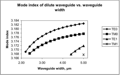
Mode index of dilute waveguide vs. waveguide width 3.166 3.168 3.170 3.172 3.174 3.176 3.178 3.180 3.182 3.184 2.00 3.00 4.00 5.00 Waveguide width, μm M o de inde x TE0 TM0 TE1 TM1
Figure 2-5. Dependence of mode effective index on ridge width in dilute ridge waveguides.
Dependence of effective indices of confined waveguide modes on waveguide width for the described layered structure are illustrated in Figure 2-5. The results are essentially similar to those for bulk waveguides of comparable dimensions. One drawback of dilute waveguides is that the discrepancy between the effective indices of TE and TM modes is increased in comparison to bulk waveguides.
2.1.2.3 Robustness of dilute ridge waveguides with respect to fabrication
variations
Robustness of the dilute ridge waveguide was accessed with respect to variations arising from wafer processing. In particular, effects of InGaAsP composition and ridge etch depth were studied. The extent of likely material composition variations wav deduced from material specifications provided by IQE, the commercial supplier of
epitaxial wafers. The bandgap wavelength for In0.79Ga0.21As0.45P0.55 material is stated as
λ=1180±20 nm. This corresponds to Arsenic content between 0.413 and 0.473 and an approximate effective index variation of about ±0.011. While waveguides fabricated with most materials within this range still support only one TE and one TM mode, the materials on the far high end of the Arsenic concentration spectrum will just start to support one higher-order TE mode. This can lead to potentially undesirable behavior in ridge waveguides. If it is in fact determined that a given wafer has higher concentration of Arsenic in its quaternaries and therefore the material has a larger overall index of refraction, the problem can be remedied by fabricating narrower passive waveguides.
We also examined the effect of varying the etch depth on the effective index of confined waveguide modes. Nominal etch depth for the designed device is 1.05 μm or 1050 nm. We calculated effective indices of ridge waveguides etched to depth of 950 nm and 1150 nm, making a generous estimate of ±100 nm deviation in etch depth. The difference in effective indices between the properly etched waveguide and an underetched or overetched waveguide was found to be only on the order of 10-4.
In conclusion, it was determined that effective waveguide index is highly insensitive to etch depth variation, but somewhat sensitive to variations in quaternary material composition. If material composition variation results in a higher index of the quaternary material, single-mode waveguide can still be fabricated by reducing the ridge width.
2.1.3 Passive ridge waveguides—Conclusions
Single-mode waveguides with a large cross-section were designed using dilute waveguide approach. Among the advantages of this method compared to single-layer
bulk quaternary material are better material quality, greater ease of material growth, and more precise control over the overall effective index of the material. Disadvantages of dilute waveguides include a more complicated layer structure causing potential
difficulties in etching and increased polarization sensitivity. Similar devices of an earlier design were fabricated with material grown in Integrated Photonic Devices and Materials Group lab by molecular beam epitaxy and were shown to support TE and TM modes.
Figure 2-6. Curved ridge waveguide.
2.2 Passive waveguide bends
Bending ridge waveguides (Figure 2-6) represent an important component in photonic circuits. Since they are inherently lossy and are used nearly as often as straight waveguides, accurate modeling is imperative. Two issues in particular need to be addressed: losses due to the waveguide curvature and losses due to mode mismatch at the transition point between waveguides of different curvature. The first problem is considerably more involved and merits a detailed discussion of available methods.
To study bent waveguides numerically, either the beam propagation methods or modal solutions approach can be applied [81, 82]. Several approaches reported in the