Deep Learning for Distributed Circuit Design
by
Hao He
Submitted to the Department of Electrical Engineering and Computer Science on December 20, 2019, in partial fulfillment of the
requirements for the degree of
Master of Science in Computer Science and Engineering
Abstract
In this thesis, we present deep learning models for designing distributed circuits. Today, designing distributed circuits is a slow process that can take months from an expert engineer. Our model both automates and speeds up the process. The model learns to simulate the electromagnetic (EM) properties of distributed circuits. Hence, it can be used to replace traditional EM simulators, which typically take tens of minutes for each design iteration. Further, by leveraging neural networks' differentiability, we can use our model to solve the inverse problem - i.e., given desirable EM specifications, we propagate the gradient to optimize the circuit parameters and topology to satisfy the specifications.
We propose two models, Circuit-Net and Circuit-GNN. Circuit-Net is a complex-valued residual network that, once trained, can accurately generate simulation results
for a specific type of circuit. Circuit-GNN is an extension of Circuit-Net, which exploits the flexibility of Graph Neural Network (GNN) to handle circuits with
different topologies.
We compare our model with a commercial simulator showing that it reduces simulation time by four orders of magnitude. We also demonstrate the value of our model by using it to design a Terahertz channelizer, a difficult task that requires a specialized expert. The results show that our model produces a channelizer whose performance is as good as a manually optimized design and can save the expert several weeks of topology and parameter optimization. Most interestingly, Circuit-GNN can come up with new designs that differ from the limited templates commonly used by engineers in the field, hence significantly expanding the design space.
Thesis Supervisor: Dina Katabi
Acknowledgments
I want to thank my advisor Dina Katabi. Her board vision and profound insight guide us through the whole project. This thesis is not possible without her generous support.
I owe many thanks to my collaborator Guo Zhang. He is a nice person. His tremendous effort in building the data generation system is indispensable for the success of this project. His diligence and optimism in research are always encouraging. I am also grateful to all the members of the NETMIT and many other folks from MIT. They provide many helpful discussions and valuable feedback for this work.
Contents
1 Introduction 15
2 Related Work 19
2.1 Learning-Based Lumped Circuit Design . . . . 19
2.2 Learning-Based Distributed Circuit Design . . . . 20
2.3 Graph Neural Networks for Relation Modeling . . . . 20
3 Methodology 23 3.1 Forward Model . . . . 23
3.2 Inverse Optimization . . . . 24
4 Circuit-Net: Learning a Single Type of Circuit 27 4.1 C ircuit-N et . . . . 27
4.2 Evaluation . . . . 28
4.2.1 D ataset . . . . 28
4.2.2 Evaluation of the Forward Task . . . . 29
4.2.3 Evaluation of the Inverse Optimization . . . . 30
4.2.4 Comparison with Past Work . . . . 31
5 Circuit-GNN: Learning a General Class of Circuits 35 5.1 Circuit-G N N . . . . 35
5.1.2 Inverse Optimization . . . . 38
5.2 Evaluation . . . . 39
5.2.1 D ataset . . . . 39
5.2.2 Evaluation of the Forward Task . . . . 41
5.2.3 Evaluation of the Inverse Optimization . . . . 43
6 Conclusion 47 A Visualizations 49 A.1 Visualization of Circuit Topologies in the Dataset . . . . 49
List of Figures
1-1 Examples of distributed circuits templates based on square resonators.
Each template has multiple control parameters like xi. . . . . 16
3-1 Illustration of our method. . . . . 23
4-1 Left: An example distributed circuit. Middle: Circuit-Net, a complex-valued
neural network model that learns the relationship between circuit geometric parameters and its transfer function; Right: An example circuit transfer
function. . . . . 27
4-2 Distributed circuits templates: (a) is a dual-band on-PCB filter composed of
6 open-loop square resonators; (b) is a single-band on-chip filter composed
of 4 open-loop square resonators; (c) is an on-chip channelizer with three
sub-filters. . . . . 28
4-3 A random example of Circuit-Net predicted transfer function for a given THz
channelizer. In the plots, dash lines and solid lines indicate the ground truth and our predictions. We display the real and imaginary parts of the transfer function in the left panel and visualize the magnitude in the right. ... 30 4-4 The transfer function of our optimized channelizer vs. the channelizer
designed by the human expert. The yellow area indicates the desired pass-bands. The Y-axis plots range from OdB to -60dB. Generally, the frequency region where the transfer function is over -6dB is considered as the pass-band
4-5 Comparison of the optimization landscapes of our model and past work. Each row contains four randomly generated 2D visualization of the gradient. In every plot, the red cross refers to the global optimum which has a zero objective value. The plots show that the gradient of our model is smooth
allowing for inverse optimization, which is not the case for past work. . . . 32
5-1 Circuit-GNN model. Step 1 maps circuit geometry to a graph; step
2 performs graph encoding using a GNN; step 3 generates a global representation of the original circuit, finally step 4 predicts the circuit's
complex-valued transfer function. . . . . 35
5-2 Data contributing to node and edge attributes. (a) shows a resonator
which is described by 4 parameters: its center position (x, y), the angular
position of its open slit 0, and its edge length a; (b) shows the definition of
gap and shift in our setting. . . . . 37
5-3 Graph examples. Each figure shows a circuit and its corresponding graph.
Note the edge between 0 and 3 disappears when these 2 nodes are far from
each other. ... .... . . . . .. . 37
5-4 Visualization of possible optimization results produced by the unconstrained
gradient descant algorithm which may give invalid circuit having self-overlaps. 38
5-5 Visualization of the allowed moving ranges for each resonator in the circuit
during one optimization step. The cyan box indicates the area where the resonator could move, and the cyan arrow shows the sampled direction during
that optimization step. . . . . 38
5-6 Qualitative results of the forward model: In each of the eight plots,
the circuit is drawn on the left and the S21 are plotted on the right. The
dashed lines and solid lines indicate the ground truth and our prediction respectively. In the circuit pictures, the position of input/output ports are indicated by two yellow arrows. We use black dashed lines to highlight the resonator pairs that are close enough to have relatively strong coupling effects. 41
5-7 Failure examples: These examples have relatively large error, however,
they still capture the trend of the 821 curve. .. . . . . 43
5-8 The transfer function of our optimized channelizer vs. the channelizer designed by the human expert. The yellow area indicate the desired pass-bands. Generally, the frequency region where the transfer function is over -6dB is considered as the pass-band. The difference from OdB is the insertion loss . ... ... ... ... .. 45
5-9 Our model versus commercial software (CST) for circuit design. Our model (in red) has higher pass-band IOU and lower insertion loss than CST (in blue). 45 A-1 All different topologies for six resonator circuits. . . . . 49
A-2 All different topologies for five resonator circuits. . . . . 50
A-3 All different topologies for four resonator circuits. . . . . 50
A-4 All different topologies for three resonator circuits . . . . . 50
A-5 Our optimized circuits topologies for each channel. Although putting four resonators as a 2 by 2 structure is standard to create a single channel filter, the positions of the slit in the resonators are very unusual compared to the human designs. . . . . 51
List of Tables
4.1 Performance of forward learning for all three templates . . . . 30
5.1 Performance of forward learning on circuits with different number of resonators. Number of training samples are also listed here.
Three-resonator and six-Three-resonator circuits are only included in testset. The table shows that the model generalizes well even to circuit topologies and sizes
Chapter 1
Introduction
Distributed circuit design refers to designing circuits at high frequencies, where the wavelength is comparable to or smaller than the circuit components. It is increasingly important since new 5G and 6G communication technologies keep moving to higher and higher frequencies. Unlike lower frequencies, where there are relatively fast tools and a large literature on design guidelines, designing distributed circuits is a slow and onerous process. The process goes as follows. An expert engineer comes up with an initial design based on desired specifications (e.g., design a bandpass filter at 300 GHz, with a bandwidth of 30 GHz). To do so, typically the engineer picks an initial template and optimizes its parameters. Figure 1-1 shows common templates used in the literature [9]. The engineer then spends extensive effort optimizing the parameters of the template (the xi's in Figure 1-1) so that the circuit satisfies the desired specifications. The optimization is done iteratively. In every iteration, the engineer sets the parameters in the template to some values, simulates the design, and compares the output of the simulation to the specifications. Each simulation takes tens of minutes during which the simulator runs mainly a brute-force numerical solution of the Maxwell EM equations. This iterative effort may turn out to be useless if the chosen template topology cannot satisfy the desired specifications, and a new template must be tried and optimized using a new set of iterations. The process can take days, weeks, or months.
X11
(a) 6-resonator filter (b) 4-resonator filter
Figure 1-1: Examples of distributed circuits templates based on square resonators. Each template has multiple control parameters like xi.
this process. Our models address both the forward and inverse design problems. The forward task takes a circuit design and produces the resulting s21 function, which
relates the signal on the circuit's output port to the signal at its input port. Said differently, the forward task produces the output of the EM simulator but using a neural network. The inverse task, on the other hand, takes the specifications, i.e., a desired s21 function, and produces a circuit that obeys the desired specifications. To
solve the inverse task, we leverage that neural networks are differentiable. Thus, given a desirable S21 and an initial circuit, we back-propagate the gradient to optimize the circuit design so that it satisfies the desired specifications.
We first introduce Circuit-Net that can optimize the circuit with a fixed topology. It is a complex-valued residual network. Given a special type of circuit, it takes the circuit design parameter as input and output the s21 function. The circuit optimization is efficiently done via applying gradient descent. Our further illustrative experiments about optimization landscape analysis explain why Circuit-Net succeeds in the first-order optimization while the prior work fails. Efficient as Circuit-Net is, it still has one main limitation that it does not work across templates which means the user needs to re-train the model every time for a new template.
To enable optimizing the circuits across a broad class of templates with one model, we proposed Circuit-GNN, a novel Graph Neural Network (GNN) model. We leverage that distributed circuits are typically designed using resonators as their building blocks. For example, it is common to use square resonators as in Fig. 1-1 ([10]), or ring resonators ([9]). By manipulating the number of resonators, their internal parameters, their relative distances, and orientations, one can design different circuits
([9]).
Ourapproach leverages this property. We model the resonators in each circuit as nodes in a graph, and their electromagnetic coupling as edges between the nodes. This allows us to design a unified model that applies across templates. Apart from sharing information across templates, this design allows the network to produce new templates beyond the ones commonly used in the field. Designing a valid circuit however by back-propagation is non-trivial because nodes have to fit in a planner space and cannot overlap. To deal with these constraints we develop a novel multi-loop gradient descent
algorithm with local re-parameterization.
This thesis makes the following contributions:
• We present Circuit-Net and Circuit-GNN which are the first models that solve the inverse distributed circuit design problem. Only
1291
tried to solve the inverse problem, but their scheme works only for circuits with one parameter, and hence is not practical. Alternatively, they propose to map the specifications to an intermediate analytical representation called the "coupling matrix", but there is no general solution that maps a coupling matrix to an actual distributed circuit design.* We present Circuit-GNN, which is the first deep learning model for distributed circuits design that works across circuits with different templates, i.e., circuits that differ in the topology and number of basic components. All past papers train a separate neural network per template
[2,
5, 6]." We introduce a novel approach for solving inverse optimizations over GNNs, where valid solutions have to maintain a planner graph with non-overlapping nodes. We do so via the re-parameterization in section 5.1.2. We believe this setup applies beyond circuit design to other graphs where nodes have a geometric and physical meaning.
" We propose an alternative approach for combining the feature maps of the nodes to generate the feature map for the whole graph in a GNN. Unlike past work on GNN where the graph is represented using the sum or pooling operation,
we propagate the information from the internal nodes to the input and output nodes, and represent the graph as a concatenation of the feature maps of the input and output nodes. We believe this is more suitable for graphs that interact with the rest of the world via specific inputs and outputs (e.g., circuits which has input and output ports). It also empirically works better for our GNN.
e We present empirical evaluations of the proposed models. The results show that our design can solve the forward task five orders of magnitudes faster than a state-of-the-art commercial simulator while maintaining accuracy. We also show the benefit of solving the inverse problem by using the model to design a Terahertz channelizer that operates at around 300 GHz and has three 30GHz-wide channels. This is a difficult task that requires a Terahertz circuit expert. The results show that our model produces a channelizer whose performance is as good as the channelizer produced by a circuit expert who spent several weeks optimizing the parameters of the template.
Chapter 2
Related Work
2.1
Learning-Based Lumped Circuit Design
Prior work on using machine learning for circuit design focuses on lumped design, where the circuit is represented as connections between lumped components: resistance, capacitance, inductance, transistor, etc. Such an approach, however, does not apply to high-frequency circuits, which require a distributed design. Further, these solutions train a separate model for each template and cannot work with unseen templates that were not used for training [3, 17, 19, 20, 21, 27, 8]. Some prior work has tried to do circuit optimization across topologies within certain regimes using genetic programming [22, 18]. These papers are different from ours both in terms of technical design and the fact that they target lumped circuits. They also face challenges including low convergence rate, slow optimization speed, and difficulty in producing meaningful designs [25].
More recently, researchers make more effort on building systems that can optimize a general family of lumped circuits instead of one select type of circuit. One idea is using reinforcement learning (RL) to learn an agent that can perform actions to improve the circuit design under any desired specifications sequentially. Another direction is to combine the traditional circuit optimization framework with deep learning models. We call them hybrid methods. Unlike the reinforcement learning methods which learn the policy from scratch, the hybrid techniques using machine
learning to assist the traditional circuit search policy where is learning is more sample efficient. For example, one work uses a learned neural network as an oracle to filter the bad offsprings generated by the evolutionary algorithm. This fast elimination of unpromising children speeds up evolution significantly. Effective as those methods are, unfortunately, they are not applied to distributed circuits design. The design space of the distributed circuit is much larger than the lumped circuit and beyond the scope of both reinforcement learning and evolutionary algorithms.
2.2
Learning-Based Distributed Circuit Design
Prior attempts at learning distributed circuit design have key limitations [2, 5, 6]. On the one hand, each of their trained models works only with a particular template and parameter setting, while our GNN model works across templates. On the other hand, unlike our model which directly predicts the values of the transfer function, s21, for different frequencies, they predict a parameterized version of the s21
function. Specifically, they leverage that the transfer function can be approximated as
s2 1(w) =:N
E
igb' where w is the frequency and ai and bi are complex parameters.Thus,instead of predicting the function 821(W), they train a neural network to predict the parameters ai and bi. This approach has several limitations. First, given a particular template even without any parameter setting, it is not clear how many parameters, as and bi, one needs to have for a good representation of the transfer function. Thus, past work, for each template, trains multiple neural networks. Second, during inference, it is not clear how to pick the best network for a particular template. Thus, past work trains an additional model that selects which network to use from the set of networks associated with that template.
2.3
Graph Neural Networks for Relation Modeling
Graph neural network (GNN) is a well-known architecture for modeling relations. Researchers have used GNN to model interaction between physical objects [28, 31, 1], chemical bonds between atoms [14, 13], and social networks [23]. GNN has also been used in computer vision for modeling the human skeleton for activity recognition [30] and person re-identification [24]. We are inspired by these prior work; however we
apply GNN to a new domain where the nodes in the graph are circuit components, and the relationships between them stem from electrical and magnetic coupling. We leverage our domain knowledge to customize GNN to our problem and ensure the model capture the underlying electromagnetics and produces valid circuits.
Chapter 3
Methodology
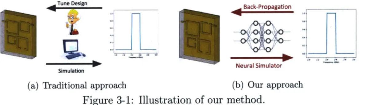
Tune Design Back-Propgtopgto
Neural Simulator
Simulation
(a) Traditional approach (b) Our approach
Figure 3-1: Illustration of our method.
Figure 3-1 illustrates our methods. We use the neural networks to replace the expert and simulator in the traditional workflow. In the forward pass, the model maps a given circuit to the corresponding transfer function (i.e., 821). In the opposite
direction, we run gradient descent to optimize the circuit parameters to produce the desired transfer function.
3.1
Forward Model
The forward model allows the designer to quickly obtain the transfer function of his/her design. It takes as input a vector x E Rn whose elements specify the values of all geometric parameters in the template. At its output, it generates a complex-valued vector y that provides a discrete representation of the circuit transfer function,
i.e., y A [ 21(W1), ... , S21(Wm)]T where {wi}i indicates the frequency samples from
the circuit working frequency Q A [Wmin, Wmax]. Our model is aim to capture the
relationship between the geometric circuit parameters x E R" and the (discretized)
transfer function y
C
C' via a neural network f, i.e. f(x; 9) ~ y(x) where 0 are the weights of our model.We use the supervised learning paradigm to train our model. The loss function contains two li-norm terms. Each of them penalizes the prediction errors in the real and the imaginary part of the transfer function respectively. Mathematical, the loss function has the following form,
£(9) E(X,Y))|R(f(x; 0)) - R(Y)|1H + |0(f(x; 0)) - a(Y)I|I (3.1)
where R and a indicate the real and the imaginary part a complex number and D is the dataset containing many samples of circuit geometric parameter and transfer function pair (x, y).
3.2
Inverse Optimization
Our model's ability to solve inverse design problem is automatically gained by the differentiable nature of the neural network. For any differentiable objective function J(y) over the transfer function y, we can apply gradient descent methods to optimize the input parameters of the neural network. In particular, consider a designer who wants to obtain a circuit geometry that satisfies a desired transfer function y*. We can define the objective function as the l2-norm of the difference between the desired transfer function and that delivered by our design, i.e. J(y) A -y - y*112. The choice
of the objective function can also change depending on the design. For example, when designing a band-pass filter, the goal is to allow signals in specific frequency bands to pass through, and block signals outside the desired bands. Since the transfer function is decided by the geometric parameters x, the objective will be imposed on x. The gradient of this objective V,J(f(x; 9)) indicates how x should be improved. Using the gradient method to optimize x via x(t+ +- x0) - VxJ(f(x(); 0)), ideally will output a geometry parameters x* with the transfer function y(x*) very close to the goal y*.
The choice of the objective function can also change depending on the design. For example, when designing a band-pass filter, the goal is to allow signals in specific
frequency bands to pass through, and block signals outside the desired bands. In this case, we can set the objective function to be the squared distance between the circuit transfer function and an ideal transfer function as shown in Equation 3.2.
j(y) = (lyil - 1)2 +
Z
yil2 (3.2)i:WiEQ* i:og(Q*
Here, Q* denotes the union of all pass-bands. An ideal transfer function satisfies
|y(W)| = 1[E-Q*] i.e. blocking all signals outside the pass-band Q*. The objective in
Equation 3.2 promotes the circuit transfer functions that are close the ideal one. The choice of objective is not unique. An alternative is using the logarithm of that ratio of the output energy between the signal in the pass-bands and the signal outside the pass-bands. This objective, shown in Equation 3.3, encourages the transfer function to have high magnitude in the pass-bands while keep low magnitude outside.
Chapter 4
Circuit-Net:
Learning a Single Type of Circuit
Forward: EM behavio predoc
0 e
Gradien Descen Iense Dese
Comnplex-vaued Fully Con enagn re ra pa rt
* IfWneay part 0.6 0.4 0.2 0.0 -0.2 -0.4 -0.6 *Sampled RetSn) *Sampled rn(sz1) 200 225 250 275 300 325 350 375 400 Frequency (G~z)
Figure 4-1: Left: An example distributed circuit. Middle: Circuit-Net, a complex-valued neural network model that learns the relationship between circuit geometric parameters and its transfer function; Right: An example circuit transfer function.
In this chapter, we introduce Circuit-Net. We first explain the model architecture and then present the evaluation results.
4.1
Circuit-Net
Figure 5-1 illustrates the neural network architecture of Circuit-Net. In contrast to past work, our model is based on a complex-valued neural network. Specifically we use fully-connected layer with complex-valued weights and complex-valued hidden units. This choice is more adequate given that signals and transfer functions have complex values. Such model allows for capturing the interaction between real and
s
xX2
(a) 6-resonator filter (b) 4-resonator filter (c) THz channelizer
Figure 4-2: Distributed circuits templates: (a) is a dual-band on-PCB filter composed of 6 open-loop square resonators; (b) is a single-band on-chip filter composed of 4 open-loop square resonators; (c) is an on-chip channelizer with three sub-filters.
imaginary values that occurs as the signal traverses the circuit. The choice of the activation function in complex-valued neural networks is more involved. The author of [26] describes three complex versions of ReLU activation, ModReLU, CReLU and zReLU. In our experiments, we use CReLU which is also the recommended choice in [26]. As shown in figure 5-1, our model also leverages the technique of residual links. In all experiments, we use a six layers neural network with a hidden size of 512. To find the best architecture for Circuit-Net, we perform a grid search on neural network hyper-parameters and try depth from four to ten, and hidden layer size from 64 to 512.
4.2
Evaluation
In this section, we first introduce the circuits templates used to test Circuit-Net.
We then present our model's performance on predicting a circuit's transfer function as
well as the performance on design a circuit. Finally, we conduct an in-depth analysis to demonstrate Circuit-Net's advantage on circuit optimization comparing to the previous state-of-the-art method.
4.2.1
Dataset
We experiment with three distributed circuits templates: a dual-band on-PCB open-loop coupling square resonator filter (figure 4-2(a)), a single-band on-chip open-open-loop coupling square resonator filter (figure 2(b)) and an on-chip THz channelizer (figure
4-2(c)).
substrate is Al203 with a thickness of 1.27mm, which is a common choice in microwave
component. The filter has 5 parameters: x1,... X5, which refer to the spacing between
resonators. All parameters take values in the range [5mm, 50mm].
Four-resonator filter. The filter operates between 200 GHz and 400 GHz. It is designed on the metal layers of an integrated chip based on IHP SG13G2 process [111. The filter has 5 parameters: X1, ... , X5, which refer to the spacing between resonators.
In our experiments, xi varies in [60pm, 100pm] while X2, -- - , X5 vary in [5pm, 50pm].
THz channelizer. Designing a Terahertz circuit is very challenging. We consider a real-world THz channelizer, which is used for a 100-Gbps-level chip-to-chip communica-tion IC. The channelizer is designed by a senior Ph.D. student in the Terahertz research group in our department. This design took him weeks and involved simulations on a supercomputer. The channelizer operates from 200 GHz to 400 GHz and has three chan-nels centered at 235, 275 and 315 GHz, each having a bandwidth of 30 GHz. As shown in figure 4-2(c), the channelizer has 3 sub-modules that correspond to the three channels. The geometric parameters of each sub-module are as follows: X1 E [1.75pm, 10pm]
denotes the width of metal; x2 E [2pm, 6.5pm], x3 E [1.9pm, 10pm], x4 E [4pm, 16pm]
define the shape of folded structure; X5, X6 E [4pm, 10pm] are the horizontal and vertical distances between different folded structures.
To train Circuit-Net, we generate labeled examples using the CST STUDIO SUIT
14],
a commercial EM simulator. Generally, it takes about 10 to 50 CPU minutes to simulate one circuit (i.e., one configuration of the parameters in the template). For every template in figure 4-2, we generate about 30,000 to 70,000 samples by using a distributed computing cluster with 800 virtual CPU cores. For each template, we use 80% of the data for training and the rest for testing.4.2.2
Evaluation of the Forward Task
We evaluate our model's prediction ability on all three templates introduced in section 4.2.1, and report the results table 4.1. As common in circuit literature, we express the error in dB. The error is computed as the mean value of the absolute difference error between the prediction value
9
and the ground truth y in dB, i.e.Table 4.1: Performance of forward learning for all three templates
Circuit Number of Examples Avg. Training Error Avg. Test Error
4-resonator filter 41087 0.22 dB 0.25 dB 6-resonator filter 32742 0.27 dB 0.30 dB THz channelizer 65850 0.57 dB 0.58 dB 0.6- 0.6-Re(521)-G IS211GT 0.4 - rn(s21 0.5- --- is1| Ours - Re(s21) Ours/ 0.2r- - In(s2n) Ours 0.4 . 0.0 - =0.3 --0.2 - 0.2--0.4 - 0.1 . 0.6. 200 225 250 275 300 325 350 375 400 200 225 250 275 300 325 350 375 400 Frequency (GHz) Frequency (GHz)
Figure 4-3: A random example of Circuit-Net predicted transfer function for a given THz channelizer. In the plots, dash lines and solid lines indicate the ground truth and our predictions. We display the real and imaginary parts of the transfer function in the left panel and visualize the magnitude in the right.
Table 4.1 shows that our model achieves a mean test error of 0.25dB, 0.30dB, 0.58dB on the three templates, respectively. Such an error is very small, indicating that our model is highly accurate. For qualitative evaluation, we visualize a random test sample in figure 4-3. The figure shows an example from the Terahertz channelizer dataset. The graphs on the left show both the real and imaginary values of the S21, whereas the graphs on the right show its magnitude. Although the Terahertz channelizer is the hardest design problem in our experiments, as we can see in figure 4-3, our model's prediction error is negligible. Visualization on other random samples performs no difference as the example we showed. In terms of the run-time for prediction, our model conducts one prediction within two milliseconds on a single NVIDIA 1080Ti GPU which is five orders faster than running one simulation using CST Studio on a modern desktop.
4.2.3
Evaluation of the Inverse Optimization
We evaluate Circuit-Net's ability to solve the inverse design problem by using it to design the Terahertz channelizer described in section 4.2.1. We optimize each sub-modules of the channelizer individually as the human expert did. For every sub-module, we use the gradient back-propagation method as introduced in section 3.2. Since the design goal here is the same as designing a uni-band filter, we employ the
~' -20 rd~ile6ponse
1
-20--40 - --6 - - ~ - u -ni6ein' -20 - -40--6-- --- - Gurs -20--40 200 220 240 260 280 300 320 340 400 Frequency (GHz)Figure 4-4: The transfer function of our optimized channelizer vs. the channelizer designed
by the human expert. The yellow area indicates the desired pass-bands. The Y-axis plots
range from OdB to -60dB. Generally, the frequency region where the transfer function is
over -6dB is considered as the pass-band of the circuit.
filter design objective function in Equation 3.2. The optimization procedure goes as follows. We first uniformly sample 32 random initial values for the geometric parameters in the design space. We then iteratively apply gradient descent 100 times on those geometric parameters in parallel using Adam [15]. We pick the geometric parameters that produces the largest objective value as our inverse design result. The whole process is fast and completes in less than two seconds on a single GPU.
We compare the transfer function produced by our model with the transfer function for the channelizer designed by the human expert using the CST simulator. figure 5-8 shows the transfer functions for both designs. The figure shows that both designs have a good inter-channel isolation and meet the pass-band requirement. Finally, we note that the human expert spent several weeks optimizing the parameters in the channelizer's template to obtain his design, This indicates that the model could save the expert weeks of work.
4.2.4
Comparison with Past Work
As explained in section 1, past neural network models for distributed circuit design learn the parameters of the transfer function as opposed to the function itself [5, 6, 2]. As a result, their approach does not lend itself to solving the inverse problem since
(a) Our model
(b) Model in [6]
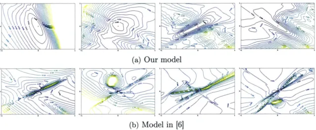
Figure 4-5: Comparison of the optimization landscapes of our model and past work. Each row contains four randomly generated 2D visualization of the gradient. In every plot, the red cross refers to the global optimum which has a zero objective value. The plots show that the gradient of our model is smooth allowing for inverse optimization, which is not the case for past work.
the gradient is not smooth. In this section, we support this intuition with empirical results.
We compare our model with the most recent prior work [6], on the 4-resonator template. We train both models on the forward task, and use the trained models to solve the inverse problem. To test their performance on the inverse problem, we randomly pick a parameter setting for the template, x*, and use the commercial simulator to generate the circuit's actual transfer function, denoted as y*. We then consider the inverse problem, where given y* the objective is to use the neural network to generate a parameter setting that satisfies this transfer function.
To evaluate the hardness of finding the optimal parameters via first-order methods, we visualize the value of the objective function near x*, which is a valid solution for the inverse problem. Since this is a high dimensional space, we leverage a 2D
visualization technique, commonly used in the literature [16, 7, 12]. Specifically, we
randomly sample two directions xi, Xk from the parameter space X, and project the
objective function on the plane created by them.
The objective function is set to 3(y) = ||y - y*||j, where y* is the desired transfer
function and y is the function returned by the model. For our model, the objective
approximates the transfer function as y(W) = EN I and returns the parameters ai's and bi's. Thus, to compute the value of the objective function, we substitute the parameters returned by the model in the above equation, then compute the objective function.
Figure 4-5 shows random examples of the optimization landscape of our model and the model in [6]. The red cross marks the projection of x*. The figure shows that our landscape has a shape close to a convex function. In contrast, the landscape of the model in [6] is highly non-convex. In our landscape, there are always large basins around x* which attract intermediate solutions to the global optimum during the gradient descent process. On the contrary, the landscape of past work is far from smooth, which can prevent the gradient method from converging to the optimal solution.
Chapter 5
Circuit-GNN:
Learning a General Class of Circuits
Step 1 - 1 Step 2 - Step3' Step 4 - GNN - Predictor
P Forward input node attributes Input edge attributes - Output node features - Output edge features
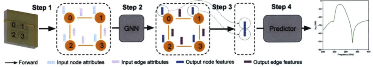
Figure 5-1: Circuit-GNN model. Step 1 maps circuit geometry to a graph; step 2 performs graph encoding using a GNN; step 3 generates a global representation of the original circuit, finally step 4 predicts the circuit's complex-valued transfer function.
In this chapter, we introduce Circuit-GNN. We first explain the pipeline of the forward model. We then present a general challenge of optimization circuits with multiple components as well as our novel re-parameterization technique to solve this issue. Finally, we discuss the experiments that demonstrate Circuit-GNN's value in both circuit simulation and circuit design.
5.1
Circuit-GNN
5.1.1
Forward Model
Figure 5-1 shows a detailed description of the forward model. The figure shows that the model has four steps, which we describe below.
STEP 1: From Circuit to Graph. In the first step, we map the circuit geometric representation to a graph, where each node refers to a resonator and each edge refers to the interaction (i.e., the electromagnetic coupling) between a pair of resonators.
A circuit having N square resonators has N raw parameter vectors. Each square resonator has a parameter vector [x, y, a, O]T as shown in Figure 5-2(a), where (x, y) is the center position of the square, a is the side length of the square, and 0 is the angular position of the slit. From this raw input, we generate a graph circuit representation with node attributes and edge attributes. Node i has attributes ni containing [ai, Q,]T which is a subset of the raw parameters. Notice that the resonator center position information are not provided to the node because the absolute positions of the circuit is meaningless. Edge attributes eij between node i and node
j
contain[0i, 6j, xi - x,, yi - y3, gip, si]T where xi - xj and yj - yj are the relative position of
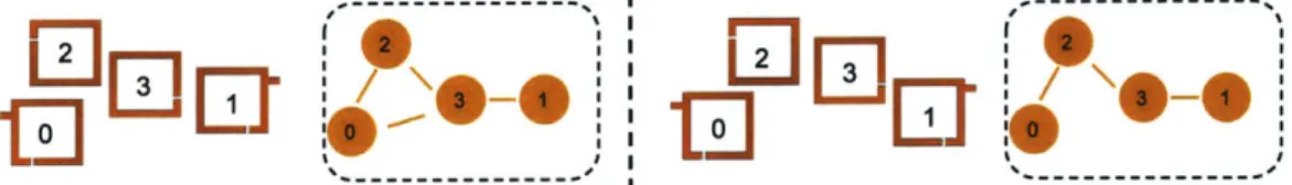
the two components. gij and sij indicate the length of the gap and shift between two square resonators as demonstrated in Figure 5-2(b). Gap and shift information are included in the edge attributes because they are important to infer the coupling coefficient between two resonators [10]. Note that not all pairs of nodes in the graph have an edge. Since electromagnetic coupling decays with distance, we leverage the data in [9] to set a threshold on distance beyond which two resonators do not share an edge. (See graphs in Figure 5-3.)
STEP 2: Graph Encoding. In this step, we use GNN to extract the nodes' and edges' features. We process the graph circuit input using a k-layer graph neural network. The th GNN layer has two sub-nets node processor
fi
and edge processorfe.
The input node features q1 are transformed to outputs as follows. First we compute the coupling effect that every resonator receives from its neighbors. We use Eij to denote the coupling effect imposed on resonator i by its nearby resonator
j.
For this edge effect Ec , we call i andj
the receiver node and sender node respectively. We use the edge processorfl
to learn this effect. Its input is the concatenation of receiver node features, sender node features and the edge attributes. Mathematically, we can calculate the edge effect from nodej
to node i as follows, et =fl(i,q
t, et').2
pap shift
(X gap
0
a
(a) Resonator (b) Gap and Shift
Figure 5-2: Data contributing to node and edge attributes. (a) shows a resonator which is described by 4 parameters: its center position (x, y), the angular position of its open slit 9, and its edge length a; (b) shows the definition of gap and shift in our setting.
--- --- --- ---
I---Figure 5-3: Graph examples. Each figure shows a circuit and its corresponding graph. Note the edge between 0 and 3 disappears when these 2 nodes are far from each other. Then the node processor is used to update the node features based on its current node features and the total coupling effect this node received. Thus the new features for
node i, q can be calculate as q =
f.
-1, E ,). In implementation, we modelnode and edge processors
f,, fl
as Multilayer perceptrons (MLP) with LeakyReLUactivation.
STEP 3: Graph Summarization. In this step, we transform all graph node
features into a fixed length global graph features g. To do so, we concatenate the features of two special nodes that represent the components that connect the circuit
to the input and output ports. Mathematically, g A [0 , g] since we have manually
indexed the square resonators connected to input/output ports as 0 and 1.
STEP 4: Prediction. Finally, in the last stage, we use the prediction network to
predict the circuit's transfer function. The prediction network outputs the prediction
y
of the s2 1 parameter for the circuit graph g. Since the transfer function iscomplex-valued we design the prediction network as a multi-layer fully connected network with residual links and complex-valued weights. The output is a complex-valued
vector y that provides a discrete representation of the circuit transfer function, i.e.,
yA [s2 1( 1),--- , S21(Wm)]T where {ow}j 1 indicates the frequency samples from the
The model represented by the above four steps is a composition of neural networks, and hence it can be represented as an end-to-end neural network. Denoting the raw circuit parameter as r E RNx4, our model is taught to capture the relationship y(r) between circuit parameters r and the true (discretized) transfer function y E C".
5.1.2
Inverse Optimization
r,
(a) valid circuit (b) invalid circuit
Figure 5-4: Visualization of possible optimization results produced by the unconstrained gradient descant algorithm which may give invalid circuit having self-overlaps.
E1E
(a) 4-resonator (b) 5-resonator
Figure 5-5: Visualization of the allowed moving ranges for each resonator in the circuit during one optimization step. The cyan box indicates the area where the resonator could move, and the cyan arrow shows the sampled direction during that optimization step.
Using the gradient descent method (introduced in section 3.2) to optimize cir-cuits with Circuit-GNN needs more elaboration. The challenge is that simply back-propagating the gradient without any constrains may lead to invalid circuit design. The feasible set of the solution space (the space for all valid circuits) is not convex. For example, in a circuit, Component A could be on the left of Component B or the right of Component B. But if we interpolate the two cases, component A and Component
B will overlap resulting in an invalid circuit. Thus, we need to design a gradient projection mechanism to make sure that during the optimization the circuit will never be outside the space of valid circuits. Or, alternatively, we can re-parameterize the circuit such that all solutions in the new parameter space are guaranteed to be valid. Among all raw input parameters, only the change of resonator center positions may cause an invalid circuit. To address this issue, we introduce a novel re-parameterization to the center positions {pi = (xi, yi)}f 1. First, we make a constraint that in each
optimization step, a resonator can move along only one of the four directions: left, right, up and down. To do this, we uniformly sample a direction vector di for each resonator from the space {(-1,0),(1,0),(0,-1),(0,1)}. Second, we compute the maximum distance mi that a resonator can move along the chosen direction. The maximum distance is decided to ensure that no two resonators collide even if all resonators move the furthest allowed. We then re-parameterize the center position of a resonator pi by the parameter qi E R as follows, pi = p* + o(qi)midi where -(-) is the sigmoid
function and p* is the original center position of the resonator. Since the sigmoid function is limited between 0 and 1, this re-parameterization ensures that the center position of a resonator does not move by more than the maximum allowable distance mi in the direction di. Figure 5-5 shows two random examples of acceptable moving ranges for all resonators in the circuit during one optimization step. Notice that the direction that a resonator can move could be different in two optimization steps since the acceptable moving ranges are re-sampled in every step. Thus, although in each optimization step the resonator can only move in one direction, in the longer run, a resonator is still able to go everywhere by zig-zaging.
5.2
Evaluation
5.2.1
Dataset
Templates with square resonators. We experiment with a broad class of distributed circuits templates based on open-loop square resonators. Each such circuit is a composition of a number of square resonators with different width, relative location, and orientation. As illustrated in Figure 5-2, each resonator is characterized
by four parameters, its center position (x, y), the angular position of its open slit 0, and the square width a. These templates are designed and simulated on the metal layers of an integrated chip based on the IHP SG13G2 process [111, a real world high frequency IC platform. The operation frequency of these circuits varies between 200 GHz to 400 GHz. In our experiments, during the data generation stage, we force all the resonators in one circuit to have an equal width a. The range of a is set to [50pm, 75pm]. Resonator center position (xi, yi) is sampled in a manner that fulfill the constraint that the gap between two nearby resonators should be in a reasonable range such as [Li, }]. The slit position 0 of each resonator is independently sampled from U[0, 27r). As for the circuit topology, it is sampled from some predefined topology patterns. An overview of all topologies in our dataset* is included in appendix A.1.
THz channelizer. It is the same channelizer introduced in section 4.2.1 as we used to evaluate Circuit-Net. However, the settings are different between evaluating Net and GNN. Previously to evaluate Net, we provide Circuit-Net with the expert design template, shown in figure 4-2(c) and ask the model to optimize the geometric parameters. In the evaluation of Circuit-GNN, we do not show the human design to Circuit-GNN and directly ask the model to design the circuit with square resonators. We will show that Circuit-GNN can design a THz channelizer using square resonators which outperforms the human design for the desired specifications. To train Circuit-GNN, we generate labeled examples using the commercial software, CST STUDIO SUIT [4]. Generally, it takes about 10 to 50 CPU minutes to simulate one circuit. In total, we generate about 100,000 circuit samples made of 3 to 6 resonators on a distributed computing cluster with 800 virtual CPU cores. We train on 80% of the data with 4 and 5 resonators, and test on the rest, including the data with 3 and 6 resonators which are 100% reserved for testing.
C--j-
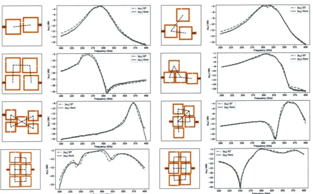
D---®r E
R.-5050 -4. -IftilW 10 z-12. 200 225250 25 30 325 330 375 400 LO!WW (50(322 2 -30 200 225 250 275 300 325 350 375 400 -4Figure 5-6: Qualitative results of the forward model: In each of the eight plots, the circuit is drawn on the left and the s21 are plotted on the right. The dashed lines and solid lines indicate the ground truth and our prediction respectively. In the circuit pictures, the position of input/output ports are indicated by two yellow arrows. We use black dashed lines to highlight the resonator pairs that are close enough to have relatively strong coupling effects.
5.2.2
Evaluation of the Forward Task
We train our model on circuits with 4 and 5 resonators and test on circuits with 3, 4, 5, and 6 resonators. For each test case, we compute the error as the mean value of the absolute difference between the magnitude of the predicted 821 parameter
y
andthe ground truth y in dB, i.e. Ed(, y) A 1 |20log0(IyIl) - 20 logio(§il)|. As
common in circuit literature, we express the error in the dB domain.
Table 5.1 shows the evaluation results of the forward model prediction. The table shows that our model achieves a mean training error of 0.92dB, and 1.10dB on circuits with four and five resonators respectively. Such an error is fairly small, indicating that a single model is able to fit the data and captures the electromagnetic properties of both 4-resonator and 5-resonator circuits.
In terms of generalization, we consider both the model's ability to generalize to circuits with the same number of resonators as those it trained on (4 and 5 resonators), and circuits with different numbers of resonators that the model had never seen (3
[]
'I'
I.-2iO 2i5 2k 63 3iC 3iS Ilk 3iS 400
I-12~ 200 225 250 275 300 325 000 375 40 ~-24 20 225 250 275 300 325 NO0 375 400 -nY(50 -4 WW OT1 -10 5fl0 -0 -5 200 222 250 2i 375 3i5 250 375 40 Fmu( CH.)
Table 5.1: Performance of forward learning on circuits with different number
of resonators. Number of training samples are also listed here. Three-resonator and six-resonator circuits are only included in testset. The table shows that the model generalizes well even to circuit topologies and sizes that never seen in training.
Number of Resonators Number of Examples Training Error Test Error
3 5790 - 1.423 dB
4 46423 0.923 dB 1.386 dB
5 37488 1.097 dB 1.785 dB
6 5859 - 2.552 dB
and 6 resonators). We refer to these two cases as same-topology-size and different-topology-size. The table shows that for topologies of 4 and 5 resonators, the test error is 1.40dB and 1.79dB. While these errors are larger than the training errors, they are still reasonably good. We believe that the difference in error between training and testing is due to limited data. With a larger training dataset, the error can be smaller. A key characteristic of our GNN mode is its ability to generalize to new topologies with a different number of resonators than those used in training. Table 5.1 shows that error on three-resonator circuits are about the same as the errors on four or five-resonator circuits, while the error of six-resonator circuits is slightly higher than that of four and five resonators. Since an error of a few dB at such high frequencies is still reasonable, we believe our model does learn the relational effects between resonators and has the ability to generalize to new circuits templates unseen in the training.
For qualitative evaluation, we visualize randomly sampled prediction results for all kinds of circuits in Figure 5-6. Every row in the figure corresponds circuits with the same number of resonators. In each raw, we display two circuits with different topologies to illustrate that our model is robust to topology variations. As we can see, the model predicts accurate S21 parameter. Some tiny error appears in the less important frequency range in the stopband which are far from the passband of the filter. Prediction results on six resonator circuits is the most difficult. Although not exactly recovering the s21, our model still accurately predicts the peak position and the filter cut-offs.
Number of Resonators Number of Examples Training Error Test Error
3 5790 - 1.423 dB
4 46423 0.923 dB 1.386 dB
5 37488 1.097 dB 1.785 dB
-10- W1% -. 0.dGT IftI 2 I 20- 5lO 2510120l i i i - -I2.I0 s-20oos--0 &. ~ -25.0 -11 _0.0i
Figure 5-7: Failure examples: These examples have relatively large error, however, they
still capture the trend of the s21 curve.
In terms of the run-time for prediction, our model conducts one prediction in 50 milliseconds on a single NVIDIA 1080Ti GPU which is four orders of magnitude faster than running one simulation using CST on a modern desktop.
Finally, we show example cases where the model fails and generates large prediction error. For further analysis, we visualize some bad examples in Figure 5-7. In these cases, our model outputs the right trend of the s21 parameters, but mistakenly predicts
the position of peaks (upside and downside) or predicts a wrong peak value.
Overall we believe these results show a significant leap in learning distributed circuit design. They enable engineers to quickly simulate their designs to ensure that they are within a few dB of the desired specifications. If more accuracy is desired, the engineers may then fine tune the final design using a commercial simulator. We will next show that the model can be used to automatically generate new circuit designs and expand the design space.
5.2.3
Evaluation of the Inverse Optimization
We evaluate our model's ability to solve the inverse design problem by comparing it with both a human expert and commercial software.
Comparison with Human Expert
We compete with a human expert on the task of designing the Terahertz channelizer described in section 5.2.1. We design each sub-modules of the channelizer individually as the human expert did. To design a sub-module which basically is a uni-band filter, we employ the filter design objective function introduced in Equation 3.2. We start from 200 random initialized circuits with different number of resonators and topologies. We then iteratively apply the local reparameterization and gradient descent steps 5000 times to optimize those circuits in parallel. At the end, we pick the circuit that
produces the best objective value as our inverse design result. The whole process is fast and completes in less than 2 minutes on a single GPU.
We compare the transfer function produced by our model with the transfer function of the channelizer designed by the human expert using the CST simulator. Figure 5-8 shows the transfer functions for both designs. Recall that the channelizer is required to have three bandpass filters, which we highlight with the shaded regions in the figure. Generally, the frequency region where the transfer function is over -6dB is considered as the pass-band of the circuit. By comparing the expert design with the automated design from our model, we see that both designs are centered perfectly in the desired frequency bands. Further, by looking at the area above the -6dB line, we see that the filter designed by our model has better insertion loss -i.e., it delivers more power in the desired bands. In appendix A.2, we show the circuit designed by the model, which is different from the human picked circuit shown in Figure 4-2(c). This shows that the model has figured out a new circuit design that differs from the one produced by the human expert.
Finally, we note that the human expert spent several weeks optimizing the param-eters in the channelizer's template to obtain his design, This indicates that the model could save the expert weeks of work. Even if the expert may not use the output of the model as is, starting from such a close design can save the expert much time and effort and this method is always fail-safe.
Comparison with Commercial Software
Commercial circuit simulators provide automatic parameter tuning tools that engineers may use to tune their design. In this section, we compare our model with CST parameter tuning, for the task of designing a uni-band bandpass filter. The filter bandwidth and center frequency are randomly chosen in [20, 40] GHz and [235, 315] GHz respectively. CST is allowed to run 450 simulations to search for a suitable design using the particle swarm method. In total, each CST design takes about 8 hours. In contrast, our model proposes only 10 design candidates. Running simulations to verify the candidates and pick the best one takes around ten minutes.
---Ieal Respons -12-0 -12 0 --- Ours -12-200 220 240 260 280 300 320 340 400 Frequency (GHz)
Figure 5-8: The transfer function of our optimized channelizer vs. the channelizer designed
by the human expert. The yellow area indicate the desired pass-bands. Generally, the
frequency region where the transfer function is over -6dB is considered as the pass-band. The difference from OdB is the insertion loss.
1.00 1.00 -- CST 0.75 - - our 0.75 --- _ur _ 0 0.50 D 0.50 U U 0.25 0.25 0.00 0.00_ 0.0 0.2 0.4 0.6 0.8 1.0 0 1 2 3 4 5 6 Pass-band IOU Insertion Loss
(a) CDF of Pass-band IOU (b) CDF of Insertion Loss
Figure 5-9: Our model versus commercial software (CST) for circuit design. Our model (in red) has higher pass-band IOU and lower insertion loss than CST (in blue).
To evaluate the resulting filters, we use two metrics corresponding to two crucial filter properties: Pass-band IOU is used to measure how close the pass-band of the circuit is to the target band. Specifically, the pass-band of a circuit is defined as the frequency region where the transfer function magnitude is higher than its
maximum magnitude minus 3db. Assume the circuit's pass-band is Q = [WL, WR] and
the pass-band wanted is Q*, the pass-band IOU is the intersection over union between
Q and Q*, i.e fluQ*. Insertion Loss is defined as the negative of the maximum
transfer function magnitude. The smaller the insertion loss is, the more power the circuit delivers in the desired bands, and hence the better the circuit is.
The results shown in figure 5-9 demonstrate that the circuits produced by our model have better pass-band IOU and insertion loss. On average across all 60 design tasks,
the circuits produced by our model have 0.80 pass-band IOU and 4.13db insertion loss while the circuits delivered by CST have 0.73 pass-band IOU and 4.92db insertion
Chapter 6
Conclusion
We present two neural network models, Circuit-Net and Circuit-GNN, that can be used both for simulating distributed circuits and automating the design process. When designing a circuit with fixed topology, Circuit-Net is a very efficient optimization tool. When the circuit topology is undecided, we propose to use Circuit-GNN who captures various circuits that differ in their topologies and sizes. We show that both models can reduce circuit simulation time by four orders of magnitude while maintaining reasonable accuracy. We believe engineers can use the models to hone in on a good design quickly. They may then leverage a commercial simulator for final tuning. We also show that both models can generate circuit designs to match the desired specifications. Interestingly Circuit-GNN can create circuits that are intrinsically different from the regular standard templates which confine today's designs. This capability is helpful for both automating circuit design and also expanding the design space.
I
Appendix A
Visualizations
A.1
Visualization of Circuit Topologies in the Dataset
AI
., -D,
[711
Il-I
12]
Figure A-1: All different topologies for six resonator circuits.
V- -- 7..1
LHFE
Figre. - 2:Aldfeettplge-frfv eoao icis
--- I '-I .1'
II2~
4--I--Figure A-3: All different topologies for four resonator circuits.
Figure A-4: All different topologies for three resonator circuits.
I]
r
-- - I