DEMOUNTABLE RESISTIVE JOINT DESIGN FOR HIGH CURRENT SUPERCONDUCTORS
Jean-Marie Noterdaeme
Research Report PFC/RR-78-11 October 1978
DEMOUNTABLE RESISTIVE JOINT DESIGN FOR HIGH CURRENT SUPERCONDUCTORS
by
Jean-Marie Noterdaeme
Burgerlijk Werktuigkundig Electrotechnisch Ingenieur
Rijksuniversiteit Gent, Belgium
1977
Submitted in partial fulfillment
of the requirements for the
Degree of
Master of Science
at the
Massachusetts Institute of Technology
May 1978
Jean-Marie Noterdaeme 1978
Signature of Author . . . . . . . .. .
Department of Nuclear Engineering, May 12, 1978
Certified by . . . . . . . .
Thesis Supervisor
Accepted by . . . . . . . . . . . . . . . .
..
. ...2
DEMOUNTABLE RESISTIVE JOINT DESIGNFOR HIGH CURRENT SUPERCONDUCTORS by
Jean-Marie Noterdaeme
Submitted to the Department of Nuclear Engineering on May 12th, in partial fulfillment of the requirements for the
Degree of Master of Science
ABSTRACT
Recent fusion reactor designs show the need for data on the resistance of demountable joints in superconductors. An experiment was set up to measure this resistance at dif-ferent pressures. The resistance is calculated from the measured decay time of the current in a superconductive loop. This method proved to be much better than the usual volt-ammeter method. Calibrated compression washers were used to provide the pressure. A resistance of 1.5xlO~9Qcm2 was achieved with silverplated joints 24000 psi. Data are provided for other contact materials.
Name of Thesis Supervisor: Lawrence M, Lidsky
3 ACKNOWLEDGEMENTS
This year of study in the United States was made pos-sible by the B.A.E.F. (Belgian American Educational Founda-tion). I am very indebted to this foundation and I grate-fully acknowledge their support.
I would like to thank my professors and especially Professor L.M. Lidsky, my thesis advisor, for the time he devoted to me. My thanks also to Professor Politzer for showing true interest in the experiment.
At the Francis Bitter National Magnet Lab the work was more directly supervised by Dr. B. Montgomery and Dr. Y. Iwasa. Dr. Montgomery helped me to focus on the parameter range the experiment was to be built for. Dr. Iwasa made the equip-ment for the experiequip-ment available and his experience was val-uable to me.
Dr. R.D. Hay of the Plasma Fusion Center shared his knowledge on the subject through very interesting conver-sations.
I am also very grateful to Mr. J. Davis and Mr. Leupold for suggestions about the engineering design of the parts.
My thanks also to the librarians in the M.I.T. libraries, and to Roger, Dick, Mike, Bruce of the N.M.L. for helping to find my way in a new environment.
4 A special word of thanks to Sheldon Rich who machined with true craftsmanship some parts and gave some very
practical hints when I made others. Thanks also to Cathy Lydon for typing this thesis,
5
DEDICATIONTo my parents.
To Michele6 TABLE OF CONTENTS Page No. ABSTRACT --- 2 ACKNOWLEDGEMENTS --- 3 DEDICATION --- 5 TABLE OF CONTENTS --- 6 LIST OF FIGURES --- 8 LIST OF TABLES --- 10 LIST OF PICTURES --- 11 CHAPTER 1. INTRODUCTION --- 12 A. Background --- 12
B. Superconductivity and Joints --- 13
C. Demountable Joints --- 20
CHAPTER 2. THE MEASUREMENT OF SMALL RESISTANCE --- 23
A. General --- 23
B. Persistent Current Decay Measurement --- 25
CHAPTER 3. THE EXPERIMENT --- 33
A. Experimental Set Up --- 33
B. The Measurements --- 38
1. Magnetic Field --- 38
2. Calibration of the Inductances --- 40
2.1 Selfinductance of the Loop --- 40
2.2 The Mutual Inductances --- 45
3. Behavior of the Ribbon Under Pressure --- 49
4. Measurements of the Resistance --- 51
4.1 Soldered Joint --- 51
4.2 Silverplated Joint --- 57
4.3 Copper Joint --- 64
7 Table of Contents (continued)
Page No. CHAPTER 4. DISCUSSION OF RESULTS AND
CONCLUSION ---1. DISCUSSION
1.1 Soldered Joint ----1.2 Silverplated Joint ---1.3 Copper to Copper Contact
---1.4 Other Contact Materials ---1.5 Components of the Resistance ---2. CONCLUSION ---APPENDIX A REFERENCES ---77 77 79 86 87 88 89 90 92
LIST OF FIGURES Figure No.
l.a. Intermediate State of Superconductive Material
---b. Mixed State of Superconductive Material
---2. Critical Characteristics of High Field Superconductors ---3. Schematic Representation of the
Mag-netic Circuits ---4.a. Current in the External Magnets
---b. Current Induced in the Loop ---c. Voltage from the Search Coil ---d. Integrated Voltage from the
Search Coil
---5. Overall View of the Experiment ---6. The Sample Holder
---7. Two Types of Joints ---8. Search Coil
---9. On Axis Magnetic Field ---1G. Recorded Voltage of the Search
Coil for Sample #4 ---11. Soldered Joint, Surface Resistance ---12. Silverplated Joint #2, Surface
Resistance ---13. Silverplated Joint #3, Surface
Resistance ---14. Recording of the Integrated Voltage
for Sample #11 ---15. Silverplated Joint #4, Induced Current
Versus Inducing Current
---Page No. 15 15 17 28 32 32 32 32 34 36 37 39
41
52 56 5860
61 63 8List of Figures (cont'd)
Page No. 16. Silverplated Joint #4, Surface
Resistance --- 65 17. Clean Copper to Copper Joint
(#5, 11, 12), Induced Current
Versus Inducing Current --- 67 18. Clean Copper to Copper Joint
(#5, 11, 12) Surface Resistance --- 68 19. Oxidized Copper to Copper Joint
(#6-10) Induced Current Versus
Inducing Current --- 70 20. Oxidized Copper to Copper Joint
(#6-10) Surface Resistance --- 71 21. Summary of the Results for the Surface
Resistance --- 74 9
10
LIST OF TABLESTable No.
1.
2.
Page No.Behavior of the Ribbon
Under Pressure --- 50
LIST OF PICTURES 11
Picture No, Page No.
1 Cross Section of the Superconductor --- 42 2 Copper Surface (5000x) --- 42 3 Middle Part of the Cross Section
(50x) --- 44 4 End Part of the Cross Section
(x)--- 44 5 Soldered Joints, Cross Section
(40x) --- 54 6 Soldered Joint, Cross Section
(.40x) --- 54 7 Detail of the Solder,
Thick-ness 40ptm (200x) --- 55 8 Detail of the Solder,
Thick-ness l0pm (200x) --- 55 9 Silverplated Surface, Unpressed,
Sample #2 (5000x) --- 82 10 Silverplated Surface, Pressed,
Sample #2 (5000x) --- 82 11 Silverplated surface, Unpressed,
Sample #4 (5000x) --- 83 12 Silverplated Surface, Pressed,
Sample #4 (5000x) --- 83 13 Idem (1000x) --- 84 14 Cross Section of the Silver Layer,
Pressed, Sample #2 (20000x) --- 85 15 Cross Section of the Silver Layer
Pressed, Sample #4 (20000x) --- 85
CHAPTER 1 12
INTRODUCTION
A. Background
When Kamerlingh Onnes liquified helium in 1908 and discovered in 1911 the superconductive state of matter he was certainly far from the thought that his pioneer work in low temperature physics might eventually be
in-strumental in the achievement of the highest temperature on earth. Superconductivity is the property of material in some range of temperature, magnetic field, current den-sity and pressure to loose all resistance. It is not our purpose to go in detail into the phenomenon. In Appendix A some books on the subject are listed together with a brief comment to guide the interested reader. In the next chapter a brief review will be given.
The most widely used material of this moment is
NbTi on which some more information can be gathered from (1). Data about the critical current density, in function of
temperature and external magnetic field can be found in
(2).
Another material which has higher critical current density and can be used in higher fields is Nb3Sn. The
material, however, is brittle and special methods have to be used to make it into useable conductors (3,4).
B. Superconductivity and Joints 13 While the phenomenon is known for many years, it is only recently that technological applications of super-conductivity have appeared. An excellent review article on superconductivity and its application has been written by B.B. Schwartz and S. Foner (5). They report on four main areas of applications: electrical motors and
generators; superconducting magnets, including those for magnetohydrodynamic and fusion power generation; power transmission and magnetic levitation for high-speed ground transportation. Focusing more on the fusion power ap-plication of superconducting magnet is the article by P. Komareck (6).
When using superconductors for application, one has to be aware of two major limitations.
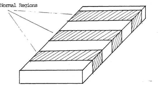
The first one is the range of parameters at which superconductivity occurs. We will only consider ourselves with atompheric pressures; for tests at higher pressure we refer to (7). At zero field, the change from normal to superconductive state is abrupt and no problem arise in defining a critical temperature and current. In the presence of a magnetic field superconductors behave in two different patterns. (A third pattern, the surface super-conductivity does not occur for superconductive material
embedded in metal). Type I superconductors go in the gen-eral case from the superconductive to the normal state
14 through an intermediate state in which normal and super-conductive regions are intermixed (Fig. la). The superconductive regions do not contain any magnetic flux (Meisner effect) while the normal regions do. When we increase the magnetic field the normal regions will grow and the superconductive regions shrink. This inter-mediate state will not occur and the Type I
superconductor will go from the superconductive to the normal state abruptly in the case of a long thick cylinder with parallel magnetic field. For type II superconductors
the transition occurs through a so called mixed state (even for a cylinder) where the normal regions form an array of narrow cylinders of material in the normal state
surrounded by the remaining superconductive material (Fig. lb).
In a higher magnetic field the thickness of those normal filaments will not increase but more filaments will be formed. Each normal filament can be seen as the center of a vortex of current. A conduction current
through the superconductor will cause the vortex line to move due to the Lorentz force. This motion would cause
an electric field, and accordingly the sample has become resistive. However, motion of those lines can be pre-Vented by metallurgical defects which pin the vortex
15
Normal Regions
Figure la Internediate State of surerconducting Naterial
Nornal Regions
Figure TB Mixed State of superconducting aterial -W0
16 lines. The sample retains its zero resistance
proper-ties up through the critical field Hc where the transi-2
tion to total normal state occurs. The domain in which a material is superconductive can be concisely shown in a
three dimensional plot. Figure 2 gives the critical
characteristics of high field superconductors (taken from Ref. 5).
The transition to normal state can occur inadvertently,
due to heat generation by friction, sudden motion of the
vortices (flux jump), etc. This would lead toun-acceptable catastrophic results in case of magnets with large stored energy. In order to avoid these problems the superconductors are stabilized by dividing the super-conductors into fine filaments and embedding it in a matrix of highly.conducting normal metal (copper or aluminum). Several approaches are persued (8). In cryostatic stab-ilization a low resistance path is provided for the current in case some part of the superconductive material goes
normal. The cooling is sufficient enough to remove the ohmic heating, to prevent the normal region to extend and the conductor will be brought back to the superconductive state. Cryostatically stabilized conductors are safe against instability due to flux jumping and to mechanical
17 J,(A/cm2) 107 Niobium-titanium alloy Nb3Sn 10 Nb3Ge (sputtered film) 104 5100 200 15 300 20 e/400 25 500 600 T (K) 4rPbMosSG 2CkG)
Critical characteristics of high-field superconductors. The critical current density Jc (on a log scale) is shown as a function of the critical upper magnetic field HC2 and the temperature Tfor three
readily available superconductors. A plot of H.2 versus T is also shown for the ultrahigh-freld compound PbMosS6. (After J. R. Gavaler and S. Foner.) Figure 2
stability against flux jumping but not against mechanical 18 instability. They rely on the fine subdivision of the
superconductor and on the embedding in a metal. The high thermal conductivity of the metal prevents a local flux instability to grow by removing the heat fast enough (ad-iabatic stabilization). The high electrical conductivity magnetically damps the motion of the vortices
so that more time is allowed for heat conduction (dynamic stabilization).
The solution of this problem brings about the second limitation. Due to technological factors in the manufactur-ing, the superconductor are available in limited length only. If longer lengths are required, one has to come up with an acceptable way of making joints. A good state of the art in joint design is given in (9). Depending on the
specific applications, some required characteristics of joints will be more emphasized than others. The report lists 6 basic characteristics.
1. Compatibility with cryogenic environment, 2. Strength,
3. Electrical characteristics, 4. Ease of fabrication,
5. Ease of inspection,
19 Depending on the types of conductors to be joined, and
the required characteristics,different bonding techniques and joint designs will be used. Where very low resistance is important and increased cross section a minor disadvan-tage one tries to come as close as possible to supercon-ductor-superconductor contact by cold pressing of twisted superconductor wire in a metal sleeve (10), some-times after stripping them first from the stabilization
material (11).
Other methods are spot welding (12,13), or
butt welding (14). In the case a continuous cross sec-tion is given the priority, a scarf joint will be the candidate joint design. As bonding techniques we list ultrasonic welding (15), explosive welding (16). Elec-tron beam welding, laser welding, are more advanced methods. Various types of soft solder, with differentjoint designs (lap, lap with reinforcement,
scarf joint) give good results and have the advantage of easy fabrication (17). There are, however,other cases where it is not limited length of the superconductor which brings about the need of making a joint. In those cases other characteristics than listed above will be required, A switch between the terminals of a superconducting coil is necessary to allow its use in the persistent mode.
20 which can be in its normal state (during the charging of
the coil) and in its superconductive state (for the persis-tent mode). For large coils the energy losses during the charging process would be too high so that an actual dis-connect is desirable (18,19). Requirements for those kind of switch., are low resistance, ease of opening and closing the switch, withstanding of a sufficient number of switching operation, reliability (19). When very low resistance, rather than a compact switch is the goal spec-ial multilam louvered bands are used with success, (20) In between the permanent joint and the switch we have de-mountable joints. This area seems to be very little ex-plored and is the main topic of our thesis.
C. Demountable Joints
There are some specific applications where semi perma-nent joints are the type of joint that would best be
suited. The joint is essentially made to carry current and its ability to be demounted is primary for non-electrical reasons (unlike the switch where the main reason is an electrical one).
A typical application is the removing of the current leadsthat charged up a superconducting magnet. These
current leads present a very high heat input due to the good thermal conductivity and the connection with the outside world. Although part of the problem was circumvented by
21 by special designs (vapor cooled leads, allowance of a low thermal gradient) the problem would be circumvented altogether if the leads could be removed. Steady state magnets for
mirror fusion machines would very much benefit from such a development.
Another application appeared as the likelihood of mod-ular design of toroidal machines became more evident. In
this application it is mainly the removal of the mechanical link that the superconductor achieves between the dif-ferent modules that is the sought after property of the de-mountable joint.
The demountable joint is a type that has its own re-quirements different from the permanent joint and the
switch. For a permanent joint very often the space allow-ance is quite strict, the low resistallow-ance, however, can be achieved by increasing the contact area ( scarf joint) and very intimate bonding between the two surfaces. For a switch the lesser bonding is compensated by more freedom on the space allowance. A demountable joint doesn't have the generous space allowance of the switch nor the very intimate bonding of the two surfaces. This is the dark side. But it is not all bad. As the joint doesn't have to be switched frequently and rapidly, more rugged mech-anical devices can be used and higher pressures applied.
22 The mechanical strength doesn't have to be provided by the
joint itself, as in the permanent joint, but can be sup-plied through the support that provides the pressure. In the next chapter, when discussing our results we will have to compare our results with data from soldered joints and switches.
CHAPTER 2 23 THE MEASUREMENT OF SMALL RESISTANCE
A. General
Every relationship containing R, the resistance is a potential basis for a method to measure the resistance. Three come easily to mind. The usual ohms law, V=RI, is the basis of several methods, which are used for a wide range of resistance measurements. The relation P = RI2 could be another basis. Measuring the power dissipated could allow to measure the resistance for a known current. Induction methods is the general name for the third series of methods. For low resistance (we are speaking of the order of 10- 8), of course, great care has to be taken in applying those methods: Contact resistance can be of the order of 10- 3.
The first method(2 1) developed into:
1. The volt and ammeter methods, where- the
vol-tage drop across potential tapsis measured for a known cur-rent through the samples. This is the most widely used method but gives often rise to problems (the voltage to be measured are of the IV range).
2. The potentiometer method; the low resistance is compared with a standard resistance of the same order magnitude. Those standard resistanceshowever, are only
24 available to 0.00010.
3. Several bridge methods are reported. The Kelvin Double Bridge is less suitable for low temperature work since the thick copper leads that are essential for its use provide a high terminal input (22).
The second method is rather theoretical than practi-cal at these power levels. For 1000A and 10- 80 the power boils off 4x10⁻³ cm3 liquid helium per second. This is a volume of approximately 2.5 cm 3/sec of helium gas at room
temperature and pressure.
The third method, although in recent years super-ceeded by the volt and ammeter method, because of its convenience is actually the most suitable one for low
re-sistance,measurements. Induction methods have definite advantages. One very important advantage is that no large
current carryng leads have to be brought down into the dewar. However, as Meaden(2 2 ) writes "electrodeless
induction methods have not as yet proved very popular for purposes of resistance measurement. This is perhaps because
they are essentially comparison methods and do not always give the resistance directly and simply. In some cases, also, the auxiliary equipment is rather elaborate, and possibly the procedure is considered laborious". For re-sistances lower than 10~ 0 this method is the only available one. Three distinct approaches are feasible of which two
measure-25 ments.
The introduction of an electrical conductor into the field of an inductor modifies the resistive and inductive components of the inductance. From this the resistivity of the sample can be calculated (23).
The second approach is that of the rotating magnetic field (24). The conductivity of the specimen is determined from the magnitude of the torque on the specimen by the rotating magnetic field.
A method that can be used for bulk materials as well as for loopsis the eddy current method for measuring the resistivity of metals. For bulk materials the method is described in (25). The method can also be used for loops. As this is the approach that was persued a more detailed description is given in the next paragraph.
B. Persistent Current Decay Measurement
With this method the resistance can be easily calculated from the decay rate of a current in a loop and the knowledge of the inductance of that loop. Lenz's law states that
- = RI + L d
26 R resistance of the loop
I current in the loop L inductance of the loop
flux due to external magnetic fields
external magnetic field t time
dS surface element. The integral is per-formed over any surface that has the loop as its boundary. The unit vector on the surface is chosen in accordance with the direction of current and the right hand rule.
Suppose the external magnetic field is kept zero, or a constant, and that the current at some initial time is
= I0. Then the solution of the equation is given by I(t) 0 et/T where 0 T = L is called the time constant ofR the system. On semilog paper the equation is a line
t
lnI = lnI - t from which slope, the time constant T can
0 T
be measured. The inductance L of the loop can be measured or calculated (we will go into more detail when describing the experiment). The resistance then follows easily from R
Onnes was the first one to use the method in 1914. More recently the method was used by Iwasa (26). As
men-27 tioned before the method is used mainly for extremely
low resistance measurements (101 Q). For our experiment, preliminary calculations based on data on the resistance of soldered joints and switches made clear that for suitable choice of the surface area of the joint and the inductance of the loop, we could achieve very comfortable time con-stants in the range of 2 to 200 sec for range of two de-cades of resistance values in the expected range.
The measurement of the decay rate of the circuit can be done in several ways. A Hall probe can be used which measures the magnetic field of the current in the loop. Another way is using a Ragowski coil. Integrating the output of the coil gives at any time the current through the loop. When the time constant of the system is large drift of the integrator can become a problem. The current can be measured at time intervals by moving a search
coil in the field of the loop and integrating the output from zero field to maximum field.
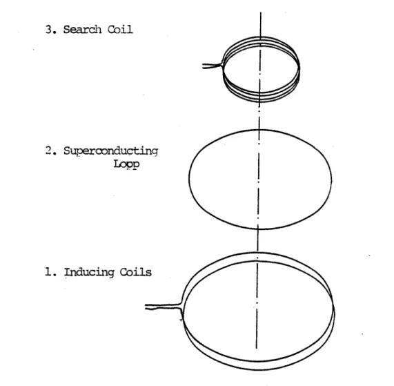
We used a fixed search coil; its voltage or integrated voltage, depending on the situation, was recorded. Let us clarify the behavior of the system. The numbers 1, 2, 3 in Figure 3 refer respectively to the external magnets, the superconductive loop and the search coil. We use as
notation L. for the self inductance of the coil i and M.. for the mutual inductance between coil i and
j.
With the3. Search Coil 2. Superconduct LCpp 1. Inducing Coi
Lng
LsFigure 3. Schematic Reoresentation of the Magnetic Circuit.
29 correct sign of the mutual inductances the circuit is gov-erned by the following equations:
VRI LdI dI 2 dI3
1 1I1 l dt +l2 dt + Ml3 dt
dI dI dI
V2-R2 2 '2 dt 2 t+ M23 dt
dI dI dI3
V-_RI
3 3 3M
l3dt-+M
2 3 dt+3
3-Those equations can be simplified in the following way. The search coil 3 is connected to a high impedance
ampli-fier so that no current is flowing 13 0. The loop 2 is closed so that there is no terminal voltage V2 E 0. Let us further consider ourselves only with the last three
equations dI dI 2 2 t 2 dt+ 212 dI dI 2
V
3 =13
t+
M23 dtWe can distinguish between two periods. First when the change of current in the external coils creates a changing flux, thus inducing a current in the loop 2 and a voltage in the search coil 3. Second when there is no
30 change in external magnetic field and the current in 2
decaysexponentially. We look at the first case. If we
dI assume = - C dI 2 2C L2 d R2 2 Solution
M
1 2CL2
I2(t)
=(-et/T)
with T = 222
Let t be time at which the current in the external
sole-0
noid 1 becomes and remains zero. This time was much lower than the time constant T (this is not true in case the current carrying velocity of the joint is exceeded. This
M 1 2C t
was never the case). Thus
I
=();
( withI (o) L2
2
12
C = t and T= , We have that I2 (t) I ().1
2
In the same approximation
I(o) M M12
V3 t 13 + L
_ 1 (0EM +
2323M1
t
Ii(o)
M
M
V3 dt = [-M 3 + 23L 12 t
31 dI2 2+
R2
2 dI2 3 23 at with I (t ) =I
(o) 2 o2 1 Solution: 1 2 12(t) e-(t-to)/T V3 23 12(t -(t-t )/T 2 t fV
3dt = -Ml31
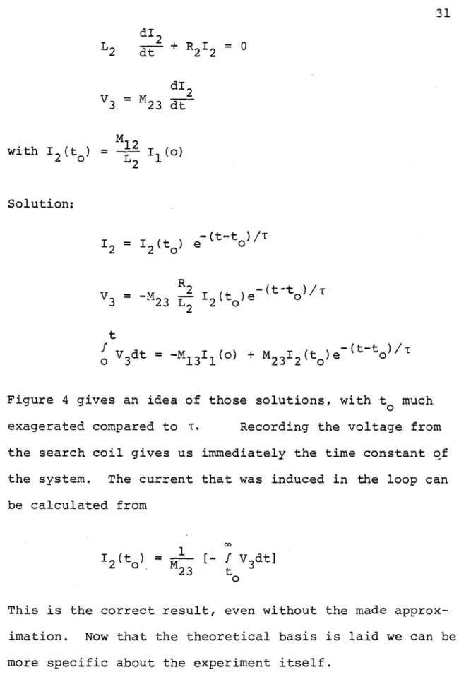
() + M2 3 2 (t )e- (t-t) /aTFigure 4 gives an idea of those solutions, with t much exagerated compared to T. Recording the voltage from
the search coil gives us immediately the time constant of the system. The current that was induced in the loop can be calculated from
12 (t
)
= [ V3dt]2 3 t
This is the correct result, even without the made approx-imation. Now that the theoretical basis is laid we can be more specific about the experiment itself.
32 Current in external Magnets
Current induced in the Loop
Voltage from the Search Coil
Integrated Voltage from the Search Coil
Figure 4.
IV
I,vE
y433
CHAPTER 3THE EXPERIMENT A. The Experimental Set Up
From the theory in the previous chapter it is clear that there are three main parts, the external magnet, the sample holder, and the search coal. These will be discussed separately after the reader has been familiarized with the complete set up.
Figure 5 gives an overall view of the experiment. The scale is 1/10. The two external solenoids, connected in
series, encircle the bottom of the deward. The sample
holder is suspended in the dewar by a 1/2" stainless steel rod. Two more stainless steel rods are used to provide a passage through the insulation material for the wires and for the dip stick (stick used to measure the liquid helium level). The search coil itself, not visible in Figure 5is located inside the sample holder; this will become clearer after the explanation of the holder. The dewar was
sup-ported by a woodenframe.
The two external magnets are commercially available solenoids (Alpha Scientific Laboratories, Inc. , Model Solenoid Coils, Serial No. 732/3340-1 and no. 732/3340-2). Internal Diameter 6 inches, External Diameter 14 inches, thickness 2 1/4 inches. Both magnets were cooled with water
34
Figure 5. Scale 1/lo Dim. in inches
35 cylinder, while the upper one rested on a wQQden support which at the same time provided the spacing between the
two magnets.
Figure 6 clarifies the design of the sample holder. The superconductive loop is supported by a thin walled cylinder of phenolic.Grooves in this cylinder secure the ribbon. The tube is partly cut out in order to support a 3/8" thick, flat stainless steel plate, again with
grooves. A second plate can be bolted to the first one with two 1/2" bolts. The ribbon is led around the cylinder
in the grooves. The joint is made by overlapping the two ends of the loop and clamping them between the two stain-less steel plates. Two type of joints can be made. Fig-ure 7 explains schematically the location of the grooves for the two types of joints.
The pressure applied on the joint can be adjusted by using one or more calibrated stainless steel compression
-washers. Solon stainless steel compression washers #8-M-89301 were used for this purpose.
Inner Diameter: 33/64" Outer Diameter: 1 - 3/16" Material Thickness: 0.089"
Deflection (flat): 0.023" Load (flat): 2600 lb. Type 301 stainless steel.
36
A
~F7
0L
U'I rZ. ............. i7VF
37N
0
0 to ~~4-L-4
38 The stainless steel rod which supports the sample holder and the search coil is soldered to the brass piece at the top of the holder. The fitting in the brass piece at the bottom is a free fitting. This way it was possible to work on the sample holder alone, whenver needed (for ex-ample to put in a new sex-ample, or to change the pressure). By unscrewing the four screws that attach the upper brass support to the plastic tube and sliding the stainless steel tube out of the lower brass holder, we can com-pletely separate the sample holder from the rest. The upper brass support, as well as the search coil remain attached to the tube. More room is now available inside the tube to bolt and unbolt the nuts and the delicate search coil can remain in a safe place.
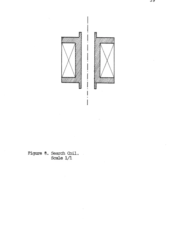
Figure 8 is a more detailed view of the search coil. The search coil was made of 45000 turns of #40 wire. Dia-meter 3.145 mills at 20*C. Resistance at 200C 1,049.00
per 1000 ft. Weight 0.02993 lb. per 1000 ft. The wires connecting the search coil to the amplifiers were a twisted pair of #24 wire. The total resistance was measured to be l9kQ of room temperature.
B. The Measurements 1. Magnetic Field
First the field produced by the magnets was measured. Ten amperes d.c.was put through the coils (in series). A
39
Figure 13. Search Coil.
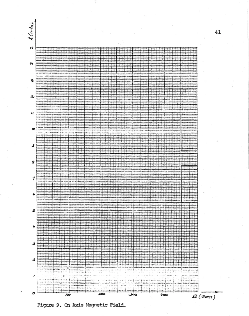
40 Hall probe was used to measure the field, the H-all probe was connected to a gaussmeter with digital read out, To locate the probe precisely in the Dewar (horizontally as well as vertically) we put it in a stainless steel tube which was held in position inside the Dewar by means of two quard rings, one at the top, in which the tube could slide, and one at the bottom, attached to the tube, sliding in the Dewar. Figure 9 gives the result on axis, the dis-tance is measured from the inner bottom of the Dewar. At the left the location of the coils is indicated schematic-ally.
2. Calibration of the Inductances 2.1 Self-Inductance of the Loop
Let us first consider some data about the loop, The ribbon was made by magnetic corporation of America
size .394"x.035it W.O. No. M14-19 Billet No. 460
Cu-Superconductor Ratio 2.6/1 # Filaments 132
Twist 1.2 turns per inch No insulation.
A typical cross section can be seen in Picture 1. Pic-ture 2 shows an S,E.M. photograph of the surface, magnifica-tion 5000.
::L:~z: -I--- ~~----W7 - -tT~~ I ~
-2oo Vc
Figure 9. On Axis Magnetic Field.
41 "N II Jo~ h 4-4 H H ill --£ if 0 Ii. -4
-6
I...
- 77 --- 1- i I . I i i , A i -t- ! i42
- 49 4-4**
0 s0 a0 trn4-N
X #43 The white band at the bottom is 10pm long, Pictures 3 and 4 show in more detail the cross section (those two pictures were made from the ends-of sample #12). The magnification is 50X,
The reader will remember that the loop was
D-shaped (flattened where the joint was clamped between the plates). An exact calculation of the inductance would be much too complicated. Calculations were made in several
idealized cases.
One filament can be approximated by a wire of ellip-tical cross section, with 2a = 0.0325 cm and 2b = 7.5xl0-3 cm. The inductance of one filament is, for a circular loop with as radius the radius of the circular part of the real loop, 4.9x10⁷ H. If all the filaments were perfectly
coupled the inductance for the 132 filaments would also be 4.9x10 7H.
The inductance for a circular loop, with a rectangular cross section, and distributed current is 1.OxlO 7H.
The inductance was finally measured with a Wayne Kerr Bridge. (Universal Bridge type B 221A Serial No. 1814). The design of the bridge is based on the transformer ratio arm principle. A full explanation of the theory of op-eration is given in Wayne Kerr Monograph No. 1, "The trans-former Ratio-Arm Bridge" available on request from the Wayne Kerr Laboratories Limited, Chessington Surrey, England. The normal range of the transformer bridge
ex-44
0 -rI U C U, 0 t.45 tends down to L = 0.9MH, A low impedance adaptor, how-ever enables us to measure inductances as low as lxlO-8 H. For certain choice of settings on the bridge and on the adapter different ranges can be selected, The measurements were made at W = 104 cycles/sec. The
skin depthat this frequency is 6 = 2 = 1.5mm. Recall that the ribbon is 10mm x 0.9mm. At this frequency the distribution of the current will be close to the current distribution in the superconducting state. We first
measured a calibrated inductance of 15x10 7H to check the procedure, then the inductance of the loop was measured, the leads were as short as possible (2 cm) and twisted. The range 0 - lyH (bridge on range 5, C on 0.1 and adaptor on range 1) was used with the first division at 0.02pH. The measured inductance was 2.OxlO7 H. The bridge could be equilibrated within 0.lxl0 7H. Then, with similar leads the inductance of a piece of wire 3cm long, c 1.5mm was measured and was within the measurement error. The con-tributor of the leads can thus be neglected. For the calculation of the resistance the measured value of L
-2.0 x 10 7H was used.
2.2 The Mutual Inductances
From the end of the second chapter it is clear that M2 3 has to be known, in order to be able to calculate the in-duced current from the formula
46,
I2 (t ) [1 V2dt],2 3 t
The mutual inductance M23 between the loop and the search coil is completely fixed by the geometry of the sample holder with the search coil, and independent of its po-sition relative to the external magnets. M2 3 is thus really invariant. The mutual inductances M1 3 and M
depend on the position of the sample holder relative to the external magnets. The sample was very precisely located
for the calibration at the maximum of the magnetic field. M
13
was measured to check the design of the search coil and N1 2 can be used to have an idea of the maximum currentthat can be induced with the formula I2 (t0 ) = I (0)I .
2
In order to measure M23 a dummy sample was made. Rather than making a joint in the loop, the two ends where
in-sulated from each other, leads were connected and brought up outside the Dewar. We put lA through the loop, inter-rupted the current and integrated the voltage from the search coil.
dI
1dI2
dI
3V
-RI
M
-i_+ .M
di+L
i3
3 3 3 13 dt 23 dt 3 dt- V 3dt= M2 3 x lA.
con-47 verter and a counter with digital display.
To measure M12 the same dummy sample was used. However, now the current was put through the external magnets, in-terrupted, and the voltage induced in the loop was inte-grated
dI dI dI3
V R I = 1 + L 2 + M
2
2
2
12 dt
2 dt+M23 dt
-
fV
2dt = 1 2 xlA.
The measure M1 3 no sample was inserted and a lA cur-rent through the external coil was interrupted. The vol-tage from the search coil was integrated,
dI1 dI2 dI
V3 - 313 = l3 + M23 t+ L3
-- vdt =M13 xA.
This method gives the correct inductances independent of any additional closed loop (like the Dewar for example). Indeed the current in such a loop is zero before the change of the magnetic field, and dies out for t so that
di.
any additional term M 3 will not contribute after
in-ij
dt
tegration. A Hall probe was located in the plane of the sample so that the sample holder could be lowered exactly
48 to the point of maximum filed of the external coils,
We obtained
M12 = 4.0 ± 0.5 x 10⁻⁵ H M2 3 = 6.0 ± 0.5 x 10 4H
N
13 = 0.15 ± 0.02H.That M1 2 agrees with the calculation can quickly be
verified.
The
field on axis for 10A through the coil
1 is maximum 340G = 0.034T. The area of the loop is approx-imately 100cm2.01m2 . Using < 12 M 21 =f 1-dS2(
surface 2
yields for the mutual inductance Ml2 1 x B x S2
or M1 2 = x 0.034 x 0.01 = 3.4 x 10⁻⁵H. The difference
12 10
being due, of course, to the fact that the field on axis is smaller than in the rest of the plane.
M13 can also be calculated. An average area is 10cm2 and we have 45000 turns. Thus M3
13 -
x 0.034 x -x0~4 x1
-0
03xlxO
x
45000 = 0.153H. A way to check M is using
V
3M
(1) 1(t ) e-(t-t
o)/[
At t=tV3 t
1
2 (t)
where 12 (t0 ) can be estimated from
I2 t)= 1 2 1 (0). 12 t0 2
49
Take, for example, Figure 10
,
which is the recorded
vol-tage of the search coil for a typical data point
V3 = - 2.7 x 10⁻³
V
t = 200 sec.
The calculated value of 1
2(to)
=
1000A. So that we can
calculate V
36.0xl1
4-3
V3 =- 200 x 1000 = - 3.QxlO
V.
The agreement of the calculated value with the measured is
a check for M
2 3'
3. Behavior of the Ribbon Under Pressure
In order to check the behavior of the ribbon under
dif-ferent pressures, two samples of ribbon approximately 5cm
long, were laid one above the other at an angle of 90*
2
and pressed together. The contact area is then 1 cm
The following table gives an overview of our findings. Note
that the yield strength (0.2% Y.S.) of NbTi is approximately
68000 psi (1) and the yield strength of copper is in
the range 10000 to 26000 psi. The pressure was applied and
removed immediately. One sample was subjected to the
pres-sure of 19400 psi for 2 hours and did not show any
dif-TABLE 1.
BEHAVIOR QF THE RIBBON UNDER PRESSURE
50
Applied Force Pressure Comment(kg) (psi)
12000
77500
Thickness reduced, large lateral
flow of the copper. Definite
im-pression marks.
The
supercon-ductors gives a pattern at the
contact surface.
9000
58000
Light pattern at the contact
sur-face, light lateral flow of the
copper, marks on the copper by
the pressure plates.
6000
38700
Pattern only at the sides of the
contact surface, light lateral
flow, marks on outer surface.
5000
32300
Same pattern, no lateral flow,
marks on outer surface.
4000
25800
idem
3000
19400
idem
2500
16000
idem
2000
12900
No more pattern at contact
surface only slight marks on
the outer surface.
1500
9700
Slighter marks on the outer
sur-face.
No marks on the outer surface. 50
TABLE 1. BEHAVIOR OF THE RIBBON UNDER PRESSURE
51 ference with the sample where the pressure was removed im-mediately.
4. Measurements of the Resistance
4.1 Soldered Joint
Our first sample was a soldered joint to check the proper operation of the whole system. The voltage from
the search coil was amplified and recorded on a x.y re-corder with the time in the x direction and the amplified voltage in the y direction. The charts were numbered in
sequence, the scales were written down, as well as the current in the external coils. Figure 10 is not from the
soldered joint (it is from sample No. 4), but is repsentative for those cases in which the voltage was re-corded. In (a) we located the pen, and in (b) we traced the zero line. The voltage oscillations in (c) are due to the fact that the current, although regulated, still has
some ripple. In (d) the current in the outer coil was interrupted, giving at first a very high voltage (out of scale), afterwards the current decays exponentially
un-til (e), where current was put through a wire wrapped around the superconductor. This drives the superconductor normal. A very rapid d gives us an out-of-scale voltage and in
dIt
(f) dI = 0. The current decayed completely to zero. May
dt
we suggest the reader compares this with the graphs at the end of Chapter 2 (Figure 4b) keeping in mind that in
---.... ---- -- --- 4-7__- -_ _ _ 1 - - 17: _____ 4~ i: .7 .-.. -.-.. ,... ... . I. .__ .... . . ... - .:S:. 7. '272.1:~1 77 1f
:
4
-
...7 -T 1 2I..:27 V. T77. :4.. 7. 7~~~~
: zv: .>-zr 7 .. 1-- --.~~~
... .... -.1
_ _ __ _ _~
l l .
_ _ _ _~....
I
...-53
Chapter 2 the time to was grossly exagerated compared to
t.The heater was put off. The current through the outer coils restored (at the same or a different value). The heater is activated again to damp out the current induced; the procedure can be started over again.
The way the joint was made was by cleaning the sur-faces with a nylon sponge, fluxing and tinning them sep-arately. We then pressed them together and heated them. A regular soldering iron was used. Solder was of the
2
50/50 type. The contact area was 3.6xm2. Microscopic inspection of the joint afterwards revealed some air
bubbles, and an uneven thickness of the solder layer (be-tween 40pim and l0pm). We refer to the pictures 5,6,7,8. Picture 5 shows a cross section of the soldered joint under a 40x magnification. So does Picture 6. The darker areas
are the filaments of NbTi. One can see an airbubble at the joint surface in Picture 6. Picture 7 shows the solder near the air bubble under a 200x magnification. The
thick-ness of the solderlayer is smaller at some places
(Pic-ture 8, same magnification 200x). The measured resistance
9
-10
were in the range 1.5xl0~9 to 2.6x10- Q so that we had
time constants from 120 to 750 sec.
The induced current
was not measured. At those time constants the drift of54
0a
U3 45 t 0i
2I
0 .f-4~
c~
* NN
*s -. * N'X" *~" ~ *- -.. ~1 .- -~ . N-- z ,2~J ~ 4 -- -*--. ~55
U) ul 4-4 0 0 P-4 a C-0I-I
K~N
-T -
T--- --- 4- 1 -~ F ~.. ~ 4.".... I- H H t~il:L FE~ i.
-~FF~
____ ~zz~T:-2z 4 - . ;- ~1~ ~+*~* 1~I
Z.., 56 k7 -i-i In '2 -44r LAI -1-=h ttt .±Ltt I L I57
the integrator would become a problem. Figure 11 summarizes
the results.4.2 Silver Plated Joint
A first sample (#2) was made in the following way. The copper surface was first rubbed with a nylon sponge until it was shiny. It was then put for 10 min. in a mixture of nitric and sulfuric acid (brite dip #2); it was
rinsed with water and dried with acetone. A silver elec-trode was used to electroplate it. The electrode was covered with cloth, and this cloth was moistened with an electrolyt. The plating was done by rubbing the
elec-trode several times gently over the surface that would pro-vide the joint. The sample was rinsed and dried with a
piece of cotton wool. The joint was clamped between the
stainless steel plates, three shims of 0.016" each were used to diminish the depth of the grooves. One compression washer was used for each of the two bolts. The voltage was measured and time constants in the range 375sec to 401 secobtained for resistances of 5.3x10-100 to 5.0x101 0. The
contact area was measured when the sample was taken out. The contact area can easily be distinguished from the rest by its shiny look. We measured 1.4cm2. In this case the joint stuck together but could easily be loosened with a screwdriver. Figure 12 summarizes the results for the
-- i--III i i1 !1 , + - - 4 00 . \0
t
'58
LztKz6~
-4T-77 '4-; CN C-i -1rIt-59 surface resistivity.
The same sample was left in the open air for one day, rebolted and new measurements were made (#3). Higher
sistances were obtained. Figure 13 summarizes the re-sults.
In order to check the reproducibility of the results, a new silver plated sample was made. In making the joint the same procedure was used except that the sample was silverplated in an electrolitic bath. The thickness of the plating was smaller. The thickness was actually so small that the color of the copper underneath the silver gave a slight tint to the plated surface. More will be
said later about the difference in plating method. The voltage was amplified and recorded.
This time measurements were also made were the vol-tage was integrated and recorded. A regular operational amplifier with a capacitor in the feed-back loop was used as integrator. Figure 14 is a typical recording of an
integrated voltage (although it is from another sample).
We again suggest the reader to compare this with the sketches at the end of the second chapter, (Figure 4d). In (a)
the drift of the amplifier was adjusted if needed. The current in the external coils is interrupted in 0 giving a sudden drop (b). The current in the loop decays
-4. - - I-. - -- - --- - --- - h---- .-.-.--- 4--. -~ 4 -.--. 4. _ L..~.u~riIrj~: ~-it-:>~ - - -~-+--- ~-.---1-~4L~L444 ~
I
60
~I4
.4 1iIT5
4A2~z~' ~' - ~ .- L-~-..-.- -to- - ,--- - -r---I i I . 4 r--.* I - ..- I -I
~DI
61
* T *~
...~. I I i I7~-H
-ii-
77
I-7--. : - -A7-7
... . . ... . ... .. .. ... ... -..H
.717
ChI
~pi~
71
...
the superconductor normal and the current goes rapidly to 62 zero. We continue to record the integrated voltage at
the end in order to check again the drift of the amplifier. 12 (t0 ) can be calculted easily from the integrated vol-tage. Remember that:
I2 (to)= [ V dt]
23 t
=-
[
0 V3dt- 0 V3 dt]23
o
o
We can plot 12 (t0 ) as a function of I . The relation should be linear as long as the current carrying capacity of the joint is not exceeded. We can also compare this to
I2(t ) = M 12 I (0)
12 t
0L
21
where we had M1 2 = 4.OxlO -5H (±0.5x10⁻⁵) L2 = 2.OxlO H (±0.lxlO )
so that = 200 35. From Figure 5 we obtain 12 = 145 Il. 2
If we take into' account the uncertainty on M
2 3,
which comes through in the calculation of 12 we obtain 12 (145 ± 12) I * There is a difference which does not fall within the uncertainties of the measurements, This dif-ference can be due to several factors. M1 2 too high, L2
I
63
H---4--I-.-.
r-4- -t~. -7' 1---I r ~ -~t~4z~4~4~
--- i--il'-: - - -. . . ~--. --- -> .--A- -...S*-.**~-~a
- ~ 0 3 0L A
1 N -- " 1 H --t = -, t
E
It
= z
Lt 4i re4Ot
I . .PA-64 too low, M2 3 too high. Remember that M12 as well as M
1 3
depends on the location of the sample holder in the magnetic field, while M2 3 only depends on the fixed geometry of the sample holder. From the integrated voltage M1 3 can be calculated using M 3 f 0 V3dt. Lower values (0.12
-13 3
0.13H) than the previous measurements (0.15H) might mean that the location of the sample holder was not exactly the
sameas when the inductances were calibrated. This would also mean a lower M1 2 which could account for the differ-ence. If we assume (worst case) that the total difference
is due to an L2 which would be larger in the superconductive state than what we measured in the normal state then it
would mean that L2 = 2.75 x 10 H rather than the measured L2 = 2 x 10 7H. The impact on this for the resistance calculating would be an increase of 37.5%. The surface resistivity are summarized on Figure 16.
4.3 Copper Joint
We also investigated a regular copper to copper joint
in order to check whether a copper to copper contact could achieve the same low resistance as the silverplated contact. The surface was prepared in the following way._7-H, ---- 4----~XL~ .---.-.-. ~. .~i.T, -____ _____
ii
L~:R-...: I. Lt~ -~ *..l-~ ~- ~ ... 1.ZIL ____ 4... -t~r r4.±~ ~ -~ ... ... 0 4-i U! tr .4-. U! C S~).2
I-, 4~4 H H Ut -'.4 - :1 - Qt
65
r~ -t 1*t66 - cleaned with a nylon sponge,
-
cleaned with acetone to remove any oil
staining.
- put in brite dip #2 for 20 min.
- cleaned with nylon sponge and water, - dried with aceton,
-
it was then put in a tank with boiling
freon.
The vapors condensed on the
surface and removed the thin residue acetone
leaves.
Four 0.016"
shims
were used and the joint clamped together
with one washer for each bolt. Figure 18 gives the results
2
for the surface resistance. The area was 1.43cm2. The
calculated 12 as a function and I appears on Figure 17.
We obtain 12
=
145 I which agrees with what we found for
the silverplated joint.
The sample was left overnight in the Dewar with the
two surfaces still in contact. We were led to the
conclu-sion that oxygen had condensed in the Dewar and formed CuO
2on
the contact surfaces on the basis of two observations:
i) the sample holder was stuck in the Dewar,
ii) when this problem was solved and the
measure-ments resumed, much higher resistances were
I~ I . ... - I - - -
-6 7
4.) -4-3 67 0 ci 14b IT
68
Th~~ 4 z~tz~zzz-z-~.~.
4...i
_______ - --tI
->1
~K
I- -- I- .-t---.--- I. :~4~-rm~ I---- I-- - I~T*~~ ~Lrj~ _________ -H--'-,- '. - --1~
~
~
~
~
- ---- --- -.--.---. -* -----.-.--*--4:.~--I.
_7 7 7-. 01 0 z LU t4 co4~ f&
69 Measurements were made with 2 compression washers
(#6), l compression washer (#7), 2 compression washers again to see if the bolting and unbolting had any effect on the measurements (#8) and 3 compression washers (#9). The
sample was left overnight in helium and some measurements were done again (#10) yielding the same results. The
re-sults are summarized in Figure 19 and Figure 20.
In order to see whether the data for a clean surface could be reproduced, new measurements were made. The
sur-face was again rubbed with the nylon sponge, put in brite dip for 15 sec, rinsed with water', dried with acetone and cleaned with freon vapor. The data are summarized on
Figure 17 and Figure 18 for comparison (#11). To see whether unbolting and rebolting the sample had any influence on the measurements,new measurements were made after the sample had been taken out, unbolted, rebolted, and put back again
(#12). Figures 17, 18.
Measurements were also made for a sample where a piece of copper (38/1000 thick) was inserted between the two
sur-faces to be jointed. We obtained R =l.5x10-80. It was not possible to relate this quantitatively to the previous measurements because when we unbolted the sample it was noticed that when the joint was made the copper piece had moved slightly so that the geometry was too complicated
K7
Lzzt ~iwt~ztz±-rw±-~4~ZZ7Z7
to 43) U0a
t7-7.4 Z~
LNiiiiiil , -i
ttttt, ::It-tt Vi- 70I
~-
71 I', zzzzzzzxzzzztrrnzzffi2zzrrz±--77:w I--- --- I '44 0i
.f-72 have two additional resistances. First one more contact re-sistance, second the resistance in the additional copper piece. The results are compatible with the assumption that for a normal joint the resistanceis due for the major part to the contact resistance.
4.4 Summary of the Results
We give briefly an overview of the different samples. #1 Soldered (50/50 solder).
#2 Silverplated.
The surface was first cleaned with a nylon sponge, put in brite dip, rinsed with water and dried
with acetone. Silverplated by hand, rinsed and dried. This sample was so clean that when we unbolted the joint it was still sticking to-gether.
#3 Same sample, allowed to oxidize in the air for 1 day.
#4 Silverplated, same procedure as for sample #2 except that the silverplating was done in an electrolytic bath.
#5 Clean copper to copper surfaces.
Cleaned with a nylon sponge, brite dip, water and aceton, freon vapors were used to re-move the film left by the acetone.