Design of a High Speed 1/f Noise Test Station
by
Kent A. Kuhler B.S.E.E University of Arizona (1990) Submitted to theDEPARTMENT OF ELECTRICAL ENGINEERING AND COMPUTER SCIENCE in partial fulfillment of the requirements for the degree of
MASTER OF SCIENCE at the
MASSACHUSETTS INSTITUTE OF TECHNOLOGY February, 1997
@1997 Kent A. Kuhler. All rights reserved.
The author hereby grants to MIT permission to reproduce and to distribute publicly paper and electronic copies of this thesis document in whole or part.
Signature of Author:
Department of Electrical Engineering and Computer Science February 3, 1997 Certified by:_
J. Francis Reintjes
Professor of Electrical Engineering Academic Thesis Supervisor
Certified by: Nancy Hartle,
Lockheed Martin IR Imaging Systems - dn •tlanvThesiispervisor
Accepted by:
, Jaur C. Smith Chairman, Committee on Graduate Students Department of Electrical Engineering and Computer Science
STAR 0
6
1997
Design of a High Speed 1/f Noise Test Station
by
Kent A. Kuhler
Submitted to the Department of Electrical and Computer Science on February 3, 1997 in partial fulfillment of the requirements for the degree of
Master of Science in Electrical Engineering
ABSTRACT
The design, operation and verification of a real time 1/f noise test station for and Infrared Focal Plane Array is described. This 1/f noise test station is based on a Personal Computer DSP card with two Analog Devices ADSP 21026 SHARC processors. The operation of the DSP card, the software written to control it, and hardware designed to interface with a Beltronics Data Acquisition System are discussed in detail.
The final system, described in this thesis, is shown to perform an accurate 8192 point FFT in real time with data rates up to 1.67 MHz.
Thesis Supervisor: J. Francis Reintjes Title: Professor of Electrical Engineering
Acknowledgments
There are many people who I wish to thank for helping me with this thesis. They have provided me with encouragement and support for which I am extremely grateful. Those most helpful to me include Nancy Hartle who managed the technical aspects of this thesis. By making resources available when I needed them, I was able to focus on the work presented and meet the goals I set out to achieve. She kept me on target and guaranteed that I was free from other tasks when it was required. Thank you, Nancy.
Ron Briggs, equally as helpful, served as an excellent resource and good friend. Many times I found myself drawing upon Ron's technical expertise in the field of electrical engineering. Through our stimulating and productive conversations, we were able to put our heads together and solve problems more easily. He is a wealth of knowledge.
Don Grays, my boss, for as long as I have known him, has provided me with encouragement and support. He has helped motivate me to see the light at the end of the tunnel on several long-range projects. He also helped make sure I was free from other tasks and prevented me from
getting side tracked.
As my academic thesis supervisor an advisor, Professor Reintjes served as a liaison between Lockheed Martin and MIT. He has offered his time and experience to make this thesis possible and to continue to strengthen the relationship my company has with the school. He kept me under his wing even through his retirement and I am grateful for that sacrifice.
My parents have granted me a life-time of love and support. For this, I can not thank them enough. Through their weekly calls from Arizona, they have motivated me and kept me reminded of the high expectations they have for me and the type of dedication and hard worked it takes to achieve the great things in life. They will never let me falter. For this, I dedicate this work to them. I would also like to thank several of my friends who have helped keep me sane throughout this
scholastic endeavor.
And finally, my new wife, who is very special to me, has shared most of what I have experienced at MIT. We were married during my final semester and most of the way through this thesis. It was a trying time for us and we have grown closer through it. We plan to continue
Table of Contents
1 Introduction ... 6
1.1 Background ... 6
1.2 Problem Statement ... ... 7
1.3 Overview of Solution ... ... 7
2.0 Comm ercial System Components ... ... 9
2.1 DSP Processor ... ... 9
2.2 DSP System ... ... 9
2.3 Comm ercial Software Packages... ... 10
2.4 Data Acquisition System ... ... 10
3 Custom System Components ... 11
3.1 Custom DAS to HSDIO Interface ... ... 11
3.2 Custom DSP Processor code... 16
3.2.1 Processor 0 code... ... 16
3.2.2 Processor 1 code ... ... 22
4 Final System Performance and Beyond ... ... 26
4.1 Final System Performance ... ... 26
4.1.1 Accuracy... ... 26
4.1.2 Data Throughput ... ... 30
4.1.3 Overall Perform ance versus Thesis Goals... ... 31
4.2 Potential Upgrades to the System ... ... 31
Bibliography ... ... 33
Appendix A Processor Code Listing ... ... 34
A.1 Processor 0 C Code for 8192 point FFT (8KFFTPO.C): ... 34
A.2 Processor 0 Assembly Code (FFTPO.ASM ): ... ... 42
A.3 Processor 1 C Code for 8192 point FFT (8KFFTP1.C): ... 44
A.4 Processor 1 Assembly Code (FFTP1.ASM ): ... 49
A.5 Comm on Include File (FFTPX.H): ... ... 51
Tables and Figures
List of Figures
Figure 1: Block diagram of working system ... 8
Figure 2: Schematic of DAS to HSDIO Custom Interface Box ... .... 12
Figure 3: Processor 0 Calculation Flow ... ... 21
Figure 4: Processor 1 Calculation Flow ... ... 25
Figure 5: Stepped Wave Form Used to Test Data Integrity...27
Figure 6: Plot of Eight Noise Spectra of Stepped Input...27
Figure 7: Noise Spectra from Ground Input Test...28
Figure 8: FFT of 5 KH z Sine W ave ... ... 30
Figure 9: Oscilloscope Photo of DAS to HSDIO Interface Operating at Maximum Speed ... 31
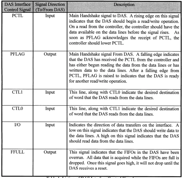
List of Tables Table 1: Listing of DAS Interface Control Signals... 13
Table 2: Listing of HSDIO Interface Control Signals ... ... 15
Table 3: Listing of D A S D ata ports... .... 15
Table 4: D ata Packing and Sort order ... ... 18
1 Introduction
1.1 Background
Seventy-five years ago, 1/f noise was first observed in electronics, and has since been extensively studied.' It is natural phenomenon that has been observed in many systems. "In fact, noise obeying the inverse frequency (1/f) law is known nowadays to exist in particularly all electronic materials and devices, including homogeneous semiconductors and junctions devices, metal films and whiskers, liquid metals, electrolytic solutions, thermionic tubes, superconductors, and Josephson junctions: and usually, irrespective of where the phenomenon occurs it goes under the generic name of 1/f noise."2 It manifests itself as a voltage or current with a power spectral density which varies with
I
fI where a usually lies between .8 and 1.3.3In Mercury Cadmium Telluride (HgCdTe) Infrared (IR) detectors, 1/f noise research is in the early stages, and measurement techniques to rapidly characterize 1/f noise are needed to obtain data for this research. In addition, the performance of imaging systems based on HgCdTe Focal Plane Arrays (FPA) can be sensitive to detector I/f noise. As a result, many specifications for FPAs require that a 1/f noise measurement be made on each and every detector in the array. To meet this need for complete FPA noise characterization a 1/f noise measurement system have been needed for both research and production.
Early attempts at building 1/f noise measurement systems have been successful but these systems take anywhere from several hours to more than a day to completely test a single FPA. The time required to make this measurement is limited by the computational power required to perform
a Fast Fourier Transform (FFT) on data from the FPA.
For many years, a class of micro processors have been developing that are heavily optimized for making the sort of calculations required for a class computations known collectively as Digital Signal Processing (DSP) which include FFTs. Now, due to the recent explosion in DSP intensive tasks such as those commonly found in an average personal computer multimedia application, and in such devices as cellular phones, modems, and home entertainment systems, the price of DSP processors has plummeted, while the power available from even the cheapest processors has grown exponentially.
DSP processor have now developed to the point where it is possible for them to perform an
FFT in real time. Performing an FFT in real time simply means that it takes less time to perform the FFT than it takes the FPA to generate the data for the FFT. A 1/f noise test station is now required that can make it's measurements in real time thereby reducing the time required to measure the 1/f noise on an FPA from several hours to its minimum of several minuets.
1 J. B. Johnson (1925), "The Schottky effect in low frequency circuits", Physics Review, 26 pp. 71-85
2 M. J. Buckingham (1983), Noise In Electronic Devices and Systems, Ellis Horwood Limited, p. 143
1.2 Problem Statement
The objective of this thesis was to develop a generic 1/f noise test station that is able to receive data from an FPA, then perform an FFT on it faster than the data for the next FFT is received. As a minimum the station must be able to make real time 1/f noise measurements on the IR line scanning FPA. The baseline for the requirements of this system was a typical high performance IR line scanning FPA that reads out multiplexed data for 480 active pixels on 16 outputs. Each output provides data for 30 active pixels and 2 reference pixels per line. Outputs are clocked at 1.4 Mega-Pixels/Sec, producing data for complete lines at a rate of 43.8 KHz. To achieve the performance goal, the 1/f noise measurement system must process data faster than the 1.4 MHz data rate of the FPA Systems previously used to measure 1/f noise on this type of FPA have included a spectrum analyzer and an older VME based DSP system. Both of these measurement systems were far too slow to perform real time data calculations. In this thesis, an advanced new approach, consisting of a combination of commercial hardware and software and custom hardware and software, was implemented to perform real time measurements on this FPA.
In order to meet the 1.4 MHz requirement, the station must be able to achieve at least two important goals. First, it must have enough computational power to perform all necessary calculations in real time. This means that in less than 6.2 ms, or the time it takes to collect 8192 samples of a single pixel, it must be able to compute an 8192 point real to complex FFT, compute the power of each of the resulting 4096 complex points, and add this power to an accumulator array. The accumulator array contains a running sum of FFT results for later use in calculating the average of multiple FFTs.
Second, it must keep up with all of the overhead associated with memory management to support both the calculations in progress and the sorting and storage of raw data as it comes in from the FPA. This quickly becomes complicated due to high data rates, and the complex data shuffling that must occur. For instance, the station must be able to store raw data in a temporary holding area as it comes in from the Data Acquisition System (DAS). At the same time, it must be able to sort and transfer data already in its temporary holding area to a processor where it is needed for calculation. In addition, it must be able to retrieve the 4096 point accumulator array, then re-store the array after it has been updated.
1.3 Overview of Solution
The final configuration of the system which achieves the goals set forth for this thesis is described in this section. The system includes both commercially available hardware and software as well as hardware and software developed specifically for this thesis. The system consists of a 120 MHz Pentium computer with a Bittware Snaggletooth DSP board. The Snaggletooth is a standard PC based ISA board with 2 40 MHz Analog Devices ADSP 21062 processors. The Snaggletooth is also equipped with an optional memory board that contains 16 megabytes of RAM and an optional High Speed Digital I/O (HSDIO) board. The HSDIO board is connected to an interface box, designed and built for this project, which allows the HSDIO board to interface with a Beltronics 16 bit Data Acquisition System. Figure 1 is a block diagram of the final system.
Software was developed for this task to use the resources of the Snaggletooth board and it's two processors in an efficient way to achieve the thesis goals. The software developed for the
system took advantage of a commercial available optimized FFT library to minimize system development time.
1/F Noise Test Station Block Diagram
2.0 Commercial System Components
2.1 DSP Processor
The system chosen for this project is based on the Analog Devices ADSP 2106X Super Harvard Architecture Computer (SHARC) family of processors. It is a new (approximately 2 years old) line of processors that has been optimized for such applications as "full-motion video, wireless digital networks, radar systems, speech recognition and satellite communications.' 4 Several of it's features made it particularly useful in this application.
Computationally, the SHARC processor is one of the fastest commercially available. For instance, it can do a 8192 point real to complex FFT in 2.83 ms5. The processor has several features that allow it to accomplish this. For instance, it can do two floating point adds, a floating point multiply, two loads from internal memory and an instruction load (from it's instruction cache) all in a single clock cycle. It has a hardware based loop counter that allows it to loop through a section of code with only a single cycle of setup time and no overhead once it enters the loop. All counter incrementing and end of loop checks are taken care of in hardware by the loop counter. For more complicated applications, the loop counter can even handle up to six nested loops at once. And finally the SHARC has a hardware based pointer system. This pointer system can automatically increment pointers by any value when the are used to access a memory location. This makes any sort of memory access extremely efficient.
Several other commercially available processors offer computation speeds that were nearly as fast or faster. However, due to the amount of data handling required for this task, the SHARC has one very important advantage. It has extensive DMA capabilities that allow several memory transfers to occur without processor intervention. In addition, the internal memory is configured such that the DMA processes can access internal memory or external memory while the processor is performing calculations on data in internal memory. This almost entirely removes the time required for memory shuffling from the minimum time required to perform an FFT.
2.2 DSP System
The SHARC processors are used in many different DSP systems by several vendors. Many types of systems ranging from more expensive and capable VME based systems to cheaper PC based system were studied for this project. The requirements of the 1/f noise system necessitated an architecture which included at least two processors to perform the calculations quickly in parallel, a large amount of fast memory that was accessible by both processors and a digital interface capable of communicating with the DAS at the rate required by the system.
The Snaggletooth board by Bittware Research Systems was chosen because it met the requirements of the system for the lowest price. The base Snaggletooth board is a PC based ISA card with two ADSP 21062 processors. It can be upgraded to have 16 MB of 1 wait state RAM,
4 Analog Devices Digital Signal Processing Data Sheet, (1994) Analog Devices, Inc.
and a high speed digital I/O interface. After some initial problems with the delivery of the product, and a few undocumented software issues, the system has performed admirably.
2.3 Commercial Software Packages
The objective of this thesis was to get a system functioning that was able to perform the required task, as quickly and cheaply as possible. For this reason, it was important that there were commercially available libraries that performed the FFTs, and as many other necessary functions as possible. Fortunately, there was a company (Ixthos) offering a library of optimized DSP routines that met the requirements for this project. In addition, Bittware and Analog devices had extensive libraries that were helpful in reducing development time.
The development effort required for this type of system is usually very deceptive. If the system developer is not intimately aware of the properties of the hardware and software involved, it quite often involves a huge learning curve. This leads to an abundance of situations where tasks that seemed trivial based your current knowledge base suddenly become impossible due to some
aspect of the system that you have just discovered. This was especially true for this system.
Again due to the young age of the Analog Devices ADSP 2106X product line, this project encountered many problems with the commercial software used by system. The initial release of the libraries purchased from Ixthos contained several bugs varying in severity. The most major was that none of the FFT routines provided produced the correct result. Their technical support was very helpful in resolving the issues, and provided a temporary patch and eventually an update to the product that solved all problems with the product. Similarly, the libraries provided by Bittware exhibited similar difficulties. Routines simply did not function properly, and there were no warnings of this fact in any of the documentation. In every case there was a patch or work around readily available to resolve the problem. Unfortunately the real loss was the debug time required to find these problems. Finding bugs in a commercial software library is extremely time consuming because of the tendency to doubt the custom code around the commercial software.
Another side effect of the infancy of these products that contributed significantly to the design time of the system was incomplete or obscure documentation. The fact that the Ixthos FFT libraries disabled interrupts from being serviced while the FFT was being performed was not mentioned anywhere in the documentation that described each of the functions. This fact was a major inconvenience and significantly altered the design of the system late in the development cycle. Bittware's documentation neglected to mention that it's software used one of the four DMA channels on both processors. These types of problems seem to be common on new systems and should be expected.
2.4 Data Acquisition System
The DAS used for this project is the latest version of the standard system used in all of Lockheed Martin IR Imaging Systems FPA test stations. The system was developed jointly by Lockheed Martin and Beltronics specifically for testing IR FPAs. At the heart of the system is a 3 MHz sample rate 16 bit Analog to Digital converter. The DAS high performance analog front end has a 30 MHz bandwidth, with four gain modes, a + 10 volt offset and a ± 5 volt dynamic range (at a gain of 1).
3 Custom System Components
3.1 Custom DAS to HSDIO Interface.
The custom interface box was designed for this thesis to convert between the different interfaces used by the HSDIO and the Beltronics DAS. Both the HSDIO and the DAS use 16 bit bi-directional interfaces, but are implemented quite differently and are completely incompatible. Both are passive (i.e. must be written to and read from), and have different handshaking methodology. In addition, the HSDIO uses 16 bi-directional lines to send and receive data, while the DAS interface uses 16 dedicated output lines and 16 dedicated input lines. In addition to simply converting the between the two interfaces, the interface box was designed with to be as fast as possible while still minimizing the probability of errors being introduced into the data.
Figure 2 is the schematic of the custom interface box, which successfully bridges the interface gap by using some simple buffers and a Programmable Logic Device (PLD). Table 1 and Table 2 are listings of the control signals and a description of their function for the HSDIO and DAS interfaces respectively.
j-4/ 7 25544252 K .2Ph2I2GN522PC ,I
Pz
-.o:
s=
2lnGND-PC P' RZ1>D-SnPE
3=4
nOSLXS 30ND-PCP,GSND-PC 11 P, 24 GNO: 8 n*IBh= PC 252P.5222. = L42-Ph55N22Cs- JlPhoIGD-SDA P 7 MID -PC nP AGND-PC nP 9GND-PC nPhioGND-PC P.IIGND-PC ... Ph2GNPC Ph 3 GND-PC PM14MID-MP P. GND-M-P P 18IGND-PC P-GND-ND-P P 2OGND-PC Ph21GND-PC P555GN52PC P MGND-PC .22542222PC PM4 5522522 IO _ _ _ -. 2 24 A4G G L. Y2 2 7,C240 U7A Y, 7•C2'• u78 2.5... 24..,... Y4 A yI ii ' A* 7- ~ um A3 YYý Alay 7ýC240 uSsF-
-i
---
p
.. ... - J ft301011 -PC , P 32CIIX-PCJ2 P 33 DIML PC J2 P. 34 07 PC > J2 P. 5 DIM P '2P MD'Oli-P J2 Ph 37 D104PC 12 PI 311) 1 PC 12 J2Ph P. . DID' 41 .10- PCPC --- ---U2A IJ P 6 O ( - -P 7ý14 ~....~~~..~..c ·· · ·~P~ WC IMPF w +5v P. 47 - Ck, - PC 7"CI4. mI INPUTOIC' K, AU4C "I0 lr I I'" IOC14 ll~L-~-~l pF'
. Ph 20M WAS. .... R
M ~1~2 Ph, 49 -Wm Sýn PC
30 7C14 UID m IPUT - -*- [(WI I Im
U41)2 1,4 INPUT Al2 ... ... WWEO
...A.. . INPUT .. .{...7...s...4An 2 .(J2 . ... Ph 49 o Ro y.s- PC
30 7"CI4 wOCVD ýýNUT a P~~mFIOO U4E IPUT Z R5 INPU JlP*hMCTLI-SD AS 32 --- f ::>2 Ph 42 E W VM -P l"C 14 w I ~ I 7ýiMOC1C) UO UWA J2 R Ph44 22222C hf :J2 Ph 43 E I~ PC -2ýCI4 wCC R114 JPh 45 Eý* Sre -P 0 ;) u 0 4-) 0cý 0 CI) (NI
hi
1ý N- T l Sthi ý Sý lIhIII C rnf~~ J i n~in~Pru-srR JI P 44 F- -SDA (W.F l*C11,,+5vU4 1II nu. EPMSOý
Rý-.i 2__ L.... 7ýC14 U.U 13 Pl···· r-t'~~'-''--~.. J2 0 10131- PC A2 Y,-f--- ~ nh~llo3P Al . 0112-7ýC20 J;P 310011-SD MI ;~ j i Ph32 DOIO: SDA R Pl33 DM D*SPh 34 DIM -SIM ji H. U ý -S DAS -i c WEE 7. ý14
PCTIL
Table 1: Listing of DAS Interface Control Signals
input
PFLAG CTL1 CTLO I/O FFULLMain Handshake signal to DAS. A rising edge on this signal indicates that the DAS should begin a read/write operation. On a read from the controller, the controller should have the data available on the data lines before the signal rises. As soon as PFLAG acknowledges the receipt of PCTL, the controller should lower PCTL.
Main Handshake signal From DAS. A falling edge indicates that the DAS has received the PCTL from the controller and has either begun reading the data from the data lines or has written data to the data lines. After a falling edge from PCTL, PFLAG is raised to indicates that the DAS is ready for another read/write operation.
This line, along with CTLO indicate the desired destination of word that the DAS reads from the data lines.
This line, along with CTL1 indicate the desired destination of word that the DAS reads from the data lines.
Indicates the direction of data transfers on the interface. A low on this signal indicates that the DAS should write data to the data lines. A high on this signal indicates that the DAS should read data from the data lines.
This signal indicates that the FIFOs in the DAS have been overrun. All data that is acquired while the FIFOs are full is dropped. Once this signal goes high, it will not drop until the DAS receives a reset.
Output
Input
Input
Input
IOS Internal Clear Internal Sync Internal Ready External Read External Write External Clear Output
Output
Output OutputInput
Input
Input
Indicates the direction of data transfers on the interface. When this signal is low, the HSDIO may be written to. When it is high, the HSDIO may be read from. This signal is controlled by the either processor on the Snaggletooth board.
A low on this signal indicates that the HSDIO interface is being cleared by either processor on the Snaggletooth board. A generic signal that can be toggled by either processor on the Snaggletooth board.
This signal indicates the status of the HSDIO FIFOs. When IOS is high, a low on this signal indicates that the HSDIO FIFOs are empty and should not be read from. A high indicates that there is data in the FIFOs and the HSDIO interface may be read from. When IOS is low, a low on this signal indicates that the HSDIO FIFOs are full and should not be written to. A high indicates that the FIFOs are not full and the HSDIO interface may be written to. The state of this line becomes invalid immediately after either a read or a write. It becomes valid again 45 ns after the falling edge of External Read on a read from the HSDIO interface or after the rising edge of External Write on a write to the HSDIO interface.
A falling edge on this signal initiates a read from the HSDIO interface. Before External Read falls, it must have been high for at least 15 ns and must stay low for at least 45 ns. In addition, the data to be read from the HSDIO becomes available 45 ns after External Write goes low and remains valid for 10 ns after it goes high.
A rising edge on this signal initiates a write to the HSDIO interface. Before External Write rises, it must have been low for at least 20 ns and must stay high for at least 20 ns. In addition, the data to be written to the HSDIO must have been present and settled on the data lines for at least 15 ns before it rises.
External Sync
Input
interface. It Can be configured to cause an interrupt on either processor on the Snaggletooth board.
A generic signal that can be used by the external device to signal the Snaggletooth board. It can be configured to cause an interrupt on either processor on the Snaggletooth board when this signal goes low.
Table 2: Listing of HSDIO Interface Control Signals
The PLD is the heart of the interface, and actively reads from and writes to both the SDAS and HSDIO depending on the state of each interfaces control lines. To achieve this, it first determines the direction of the data flow by the state of the HSDIO's IOS line. Because this line exactly matches the functionality of the DAS I/O signal, except for polarity, the PLD inverts this signal and passes it directly to the DAS. If IOS is high, the PLD attempts to read data from the HSDIO interface and write it to the DAS.
To write to the DAS, the state of it's CTLO and CTL1 lines must first be set to determine the destination of the data to be written. Table 3 lists the destination of the data for each of the possible combinations of CTLO and CTL1. Because the HSDIO interface does not have the facilities to accomplish this, the PLD must read two words from the HSDIO interface for every one word it writes to the DAS. The first word is not sent on to the DAS. Instead, Bits 15 and 16 are latched by the PLD to drive CTLO and CTL1 respectively. The second word is then passed on to the DAS. The reduction in throughput that this causes is negligible because very few words are written to the DAS at the beginning of each FFT test to configure it.
I It nI I it 13 I 15114 I uutput wora I
0 1 Bit 16 Bit 15 Bit 14 Iteration Count
1 0 Bit 16 Bit 15 Bit 14 Pixel Count
0
0
1
1
1
Gain
0 0 0 0 1 Offset
0
0
1
0
1
Delay
o
o
0 1 1 Configuration wordTable 3: Listing of DAS Data ports
To begin the process of writing to the DAS the PLD first monitors the state of the HSDIO's Internal Ready line. If it is high, then data is available for reading. If it is low the PLD simply waits until it goes high. The handshaking proceeds as follows: if Internal Ready is high (The FIFOs are not empty) and Internal Clear is high (HSDIO is not being cleared), the PLD lowers External Read. 160 ns later it raises External Read. At the same time it latches the data from Bit 16 on CTL1 and the data from Bit 15 on CTLO. 40 ns after that it checks the state of Internal Ready and Internal Clear again. If both are still high, it starts the second read by lowering External Read. 160 ns later it begins the DAS write cycle by raising PCTL. It holds in this condition until the DAS lowers PFLAG acknowledging the write command. When the PLD receives the low signal on PFLAG it immediately lowers PCTL and raises External Read. When the DAS Raises PFLAG again, this
signifies the end of the process. The PLD begins the cycle once again by monitoring the state of Internal Ready.
If the IOS line is low, the PLD must read data from the DAS and write it to the HSDIO. To begin this process it once again monitors the status of the Internal Ready line. If it is high, then the HSDIO's FIFOs have enough room in them to accept more data. If it is low the PLD simply waits until it goes high. The handshaking proceeds as follows: if Internal Ready is high (The FIFOs are not full) and Internal Clear is high (HSDIO is not being cleared), the PLD raises PCTL and lowers External Write. When the DAS responds by raising PFLAG, meaning the data requested is available on the data lines, the PLD lowers PCTL and raises External Write. To end the process the PLD waits for 120 ns then checks to see if PFLAG is low. If it isn't, the PLD continues waiting until PFALG goes low. At this point the process starts over again.
The remaining lines on both interfaces (FFULL on the DAS and External Clear, External Sync, Internal Clear and Internal Sync on the HSDIO) are used for communicating special situations. FFULL on the DAS indicates that it's FIFOs are full. If this occurs during a test, then data is being generated faster than it is being processed, and the test being performed exceeds the maximum rate allowed by the system. The PLD senses FFULL and if the HSDIO is currently reading from the DAS it lowers External Clear. This halts any further data transfers to the HSDIO and generates an interrupt in Processor 0 on the Snaggletooth board.
External Sync set low by PLD to indicate to the HSDIO board that the DAS has been sent a reset and has acknowledged it's completion. When External Sync goes low, an interrupt is generated in both processors on the Snaggletooth board. Because every command sequence sent to the DAS ends with a reset, this interrupt informs the processors when the DAS has received a command sequence and is ready for further action. External Sync is raised again by the PLD when either the HSDIO interface is cleared (Internal Clear goes low) or a processor lowers Internal Sync.
3.2 Custom DSP Processor code.
To process the data fast enough to keep up with the data coming in from the DAS, great care must be taken in how the data gets handled once it is read from the HSDIO interface. The great bulk of the work done for this thesis involved perfecting this process given the characteristics of the ADSP 2106X processors and the various pieces of commercial software used for the project. Figures 3 and 4 show flow diagrams for the working software for processor 0 and processor 1 respectively.
The tasks the two processors perform are slightly different for 2 major reasons. First, the HSDIO interface can only be written to by processor 1 and read from by processor 0. Second, 2 clock cycles per data point could be saved by having processor 0 unpack the raw data from the DAS for both processors while processor 1 accumulates the power from both FFTs' results.
3.2.1 Processor 0 code.
The flow for processor O's program is as follows (see Appendix A.1 for a listing or Figure 3 for a flow diagram): processor 0 starts by setting FLAGO. FLAGO is a readable by the host PC and is used to inform the PC when the DSP processors have finish the FFT's. Next, processor 0 starts it's initialization routine. This does several tasks. First, it sets the processor up in the proper state.
The ADSP 2106X SHARC processor has several registers that determine the characteristics of it's operation, such as how it accesses external memory, which interrupts it responds to and a variety of other features. It then initializes and configures the DMA channels that will be used during the test. It's last task is to initialize all of the variables that will be used during the test.
After initialization, processor 0 waits for processor 1 to finish it's initialization. It does this using a message register. Each of the processors has 8 message registers that are specifically for inter-processor communication. Several of these registers are used throughout the program to keep the two processors synchronized. The registers are used just like handshake lines on a digital interface. An example of their usage is as follows: processor 0 writes a specific value to a message register in processor 1. It then monitors it's own corresponding message register for a response. Processor 1, after finding that the proper value in it's message register, writes the proper response value in the corresponding message register in processor 0. After receiving the proper value in it's
message register, each processor clears that message register so that it can sense the next use of that message register. In this manner, both processors can be synchronized to a particular point in their respective programs independent of which processor reaches the synchronization routine first.
Processor 0 then initializes it's link port interface with the HSDIO interface. It waits until this point before opening the link to the HSDIO interface, because it must be sure that the HSDIO interface has been reset. Processor 1 resets the HSDIO interface just before the most recent synchronization in it's own initialization routine. At this point both processors are ready to begin processing. Processor 0 calls it's start_das 2 hsdio routine which begins by waiting for the reset_comp flag to be set.
The reset_comp flag is set by another routine (hsdioisr) that is an interrupt service routine. This interrupt service routine is called by the processor when an interrupt is generated by the HSDIO interface. When the hsdio isr routine is called it checks the HSDIO's status word. The status word indicates what signal from the DAS/HSDIO interface box caused the interrupt. For this project, the HSDIO interface is configure such that, two things can cause it to generate an interrupt, and both are as a result of signals from the DAS/HSDIO interface box. The first is when the DAS/HSDIO interface raises the External Clear signal. The DAS/HSDIO interface raises this signal to indicate that the DAS has overrun it's FIFO. This indicates that the 1/f noise test station is not keeping up with the data being generated.
The second signal that can an interrupt is the External Sync signal. The HSDIO/DAS interface raises this signal after the DAS acknowledges that it has been reset. When the hsdio_isr receives this signal it sets the reset_comp flag and exits.
After the start_das_2_ hsdio routine sees the reset_comp flag, it resets the HSDIO interface and configures it to read data from the DAS. It then transfers one data point plus ten frames of data from the DAS and discards it. The single data point is discarded because the HSDIO interface has a pipeline that contains a bogus piece of data after a reset. The ten frames of data are discarded because of the possibility of the first several data points from the DAS being noisier than data that is taken later. This sort of start up phenomena is common in the Beltronics style DAS's and must be corrected for.
When this initial data transfer is complete processor 0 begins transferring in the first full set of data. Table 4 lists the order in which the data, which is packed and unsorted, is transferred in from the DAS. Because of this ordering, data can not be processed as soon as it is transferred in. Instead, the first full 32 channel by 8192 data point data set is transferred in. It can now be
processed while the next full data set is transferred in. Once the first data set is in, the start_das 2 hsdio routine completes and processor 0 is ready to start processing FFTs.
2 15 16 17 131071 131072 (8192*32/2) 4 30 32 2 30 32 1 1 1 2 8192 8192 3 29 31 1 29 31 1 1 1 2 8192 8192
Table 4: Data Packing and Sort order
At this point, two loops are initiated. The outer loop counts the number of averages or complete data sets processed. This loop is executed as many times as specified by the host PC. At the beginning of each average, the data for the first two pixels is moved from global memory to processor O's local memory. In this transfer process, the data is properly sorted, but is not unpacked. Also, before the last average, processor 0 stops reading data from the HSDIO interface. Both processors can then perform FFTs on the last data set at their maximum rate without waiting for data to be acquired by the DAS. This can save significant time when performing FFTs on FPAs that have very slow data rates. For the FPA this system was designed for, the time savings are minimal.
The inner loop counts the number of pixels processed in the current data set. This loop is executed once for every two pixels in a single frame of data. The number of pixels in a frame of data is also downloaded by the host PC. Inside this loop the processor starts by reading the next segment of data from the HSDIO interface. The size of the segment of data is the same as the length of the FFT, even though two FFT are being processed (one by each processor). This is because the two data points are packed into each word read from the HSDIO interface, as in Table 4.
Next, processor 0 calls a routine called decode_raw (see Appendix A.2 for a listing of this routine). Decode_raw is an assembly routine written for this project that unpacks the raw data and performs all of the operations on it that are necessary to prepare it for processing. Below is a listing of what this routine accomplishes on each raw data word:
* Load window value
* Unpack least significant 16 bit word from 32 bit raw data word * Convert from integer to floating point
* Multiply by window value
* Unpack most significant 16 bit word from 32 bit raw data word * Convert from integer to floating point
* Multiply by window value
* Store in processor O's local memory
By carefully designing this routine, it was made to perform all of this in just three clock cycles per data point. The completion of this routine leaves each processor with a complete set of data in it's local memory that is ready for processing.
At this point the two processors are re-synchronized. Processor 0 then initiates FFT routine which takes approximately 13.8 clock cycles per data point.
After the FFT, if this is not the last two pixels data in the current average, the next set of raw packed data is read into internal memory. The raw data is not transferred in for the last two pixels processed because the last segment of data in the next data set is still being transferred in from the DAS. As explained earlier, because of the way the data is sorted, processing cannot begin on a data set until it has been completely transferred in from the DAS. Unfortunately, the processor must wait for this DMA transfer to complete before continuing. This is because either the external bus or the array that holds this data is in use during the entire time spent inside the loops. This transfer from external memory takes two cycles per data point.
The last step in the loop is to wait for the data transfer from the DAS to complete, then transfer this segment of data out to external memory. Since initiating this transfer was the first step in the loop, this allows the processors to process data during the entire time that data is being transferred in from the DAS. The only time when data is not being transferred in from the DAS is while the segment of data is transferred out to external memory. This only takes two clock cycles per data point, and it's effect is minimized by the FIFOs on both the DAS and the HSDIO interface.
This marks the end of the inner loop. Counting up all of the cycles used in the inner loop gives a good estimate of the maximum speed that may be achieved by the system. The steps listed above total 20.8 processor clock cycles per data point. With a processor clock speed of 40 MHz, this gives a maximum data rate from the FPA of:
40 MHz clock rate/20.8 cycles per data point per processor*2 processors = 3.84 MHz.
If the inner loop terminates at this point, marking the completion of an average, processor 0 checks to see if the DAS has overrun it's buffers. If it has, processor 0 uses it's flags to indicate to the host PC that it encountered an error, and that the DSP processors have stopped processing. Processor 0 then immediately halts. The DAS data overrun check is performed here for two reasons. First, because the overrun occurred on the data that is about to be processed, all results from FFTs that have already been calculated are uncorrupted and can potentially be salvaged (although no provisions have been made for this in the existing code). In addition, it allows for the simple addition of a future optimization. If processor 0 detects a data overrun, it could request that processor 1 resets the DAS, then it could collect another set of data. This would allow the system to operate in the mode where it collected data, then processed it in serial, which would trade off total test time for a higher maximum data rate from the FPA.
After the completion of both loops, processor 0 waits for processor 1 to finish up all of it's final calculations. It then calls the final_power calc routine which converts the accumulated power results to average bits RMS. It is left up to the host PC to finish converting the results to the most
frequently used units of Volts per root Hz. This is because this conversion involves information that the DSP processor does not have such as DAS analog gain and FPA frame rate.
At this point processor 0 signals the host PC that it has finished performing the required FFTs and terminates. The host PC can then retrieve the results it requires from the Snaggletooth boards external memory when the PC senses that the processors have completed their task.
Processor
0
Calculation Flow
3.2.2 Processor 1 code.
The flow for processor l's program is similar that of processor O's but is far simpler. A description of it follows (see Appendix A.3 for a listing, or Figure 4 for a block diagram). Processor 1 starts by running it's initialization routine (initialize_memory). This routine is similar to the processor O's initialization routine and begins by setting up the processor's configuration registers. Processor 1 then initializes and configures the DMA channels that will be used during the test. And finally, it initializes all of the variables that will be used during the test. This includes initializing the accumulator array to zero.
When the initialization routine returns, processor 1 calls the HSDIO initialization routine (initialize_hsdio). This routine resets the HSDIO interface then configures it to write to the DAS. It also initializes the link port through which the processor is able to write to the DAS via the HSDIO interface.
At this point the two processors synchronize by the method described in the section 3.2.1. Processor 1 then calls the reset_sdas routine which simply writes the value to the HSDIO interface that resets the DAS. This is the extent of the communication required by this processor with the DAS as the software is currently configured. To implement the upgrade described in section 3.2.1 that would allow processor 0 to request that processor 1 reset the DAS upon sensing that the DAS had overrun its FIFOs, the reset_sdas routine would have to be rewritten. It would have to be implemented as an interrupt service routine that was callable through the ADSP 2106X's virpt feature. This feature allows one processor to cause an interrupt on another processor, and give it the address of the interrupt service routine that should handle it.
Processor 1 then enters two nested loops similar to the ones described for processor 0. The outer loop counts the number of averages that have been completed, while the inner one counts the number of pixels completed within the current data set. Upon starting each of these loops, processor 1 sets the status of it's FLAG 0 and FLAG 1 for the pixel number loop and the average number loops respectively. It sets the FLAG 0 based on the current pixel number and FLAG 1 on the current average. Because these flags control LED's on the Snaggletooth board, they provide the system operator with valuable visual feedback on the operational status of the system.
Immediately after entering the loops, processor 1 synchronizes with processor 0. It then starts a DMA process that transfers the previous accumulated results out to external memory. Next it waits 40 cycles then starts a DMA process that loads the next 2 pixels accumulated results into it's local memory. This seemingly simple set of memory transfers is configured this way for several complicated reasons. Processor 1 uses a routine called add to_accum to add the results from both processor's current FFT results to the accumulated results from their respective pixels previous FFTs. This routine performs the operation in place, which simply means that it reads the previous accumulated results from the same location that it writes the new accumulated results to. The result of this is that the location from which the first DMA process reads the previous pixels accumulator is the same as the location that the second DMA process writes the new pixels accumulator.
The intent of starting these DMA processes at this point is that they complete during the time that the FFTs are being computed, while the external bus is not in use. During the rest of the loop, the external bus is in heavy demand, and any use of it would increase the minimum time required to compute each FFT. Because the two memory transfers are acting on the same memory location, it is very important that the DMA process that is reading the next accumulators results into the array do so after the results from the previous accumulation have been written to external
memory. Normally the two DMA processes would be done serially, with the first DMA process generating an interrupt upon completion. The interrupts service routine would then start the next DMA process. In this case, however, interrupts are not an option because the commercial FFT library takes liberties with the configuration of the processor that require them to disable interrupts from occurring while the routine is being executed. This is to prevent any interrupt service routine from trying to execute with the processor so configured.
In this case, an alternative to using interrupts is to take advantage of the way that the SHARC processors DMA engine decides which DMA process has access to the external bus. The four external DMA channels are 6, 7, 8 and 9. The DMA engine gives priority to the lowest numbered channel that is requesting access to the external bus. The DMA process that is transferring the previous pixels data out to external memory is performed on the lower channel number. Therefore, it is always given access to the external bus, and is guaranteed to complete first without interference by the second DMA process. The 40 cycle delay between starting the two process is to give the first process time to get started, and give some buffer in case there are any delays that case the first process to stall for a short period of time.
Immediately after the second DMA process is initiated, the processor begins executing the FFT, which takes 13.8 cycles per data point. When processor 1 finishes the FFT, it verifies that both DMA processes have completed their transfers. When they are complete, processor 1 calls an assembly routine called add_to_accum (see appendix A.4). This routine performs the accumulation process on the FFT results. Below is a listing of the what this routine accomplishes:
* Load the real FFT results into a register * Load the imaginary FFT results into a register * Square the real portion of the FFT
* Load the accumulator results into a register * Add the squared real portion to the accumulator * Square the imaginary portion of the FFT
* Add the squared imaginary portion to the accumulator * Store the new accumulator
Again by carefully designing this assembly routine, the processor is able to perform all of this in just three clock cycles per data point. The routine performs these operation on the results from Processor l's FFT first. Next it verifies that processor 0 has completed writing it's FFT results in processor l's local memory, then performs the same steps on processor O's results.
During the last average, if the host PC set processor l's debug flag, processor 1 stores the results of last data sets FFT in external memory. This can be useful for debugging many aspects of the system. When processor 1's debug flag is set, at the completion of the program external memory contains the average FFT results, the result of the last FFT and the last data set. If the debug flag is not set, external memory contains the average FFT results, and the last two data sets. Typically this flag should not be set because it requires additional time to transfer the last FFT's results to external memory.
Upon completion of these two loops, processor 1 transfers the last accumulator result from local memory to external memory. Next, processor 1 synchronizes with processor 0 to let it know that all of the data is now available in external memory. Finally, Processor 1 turns off its flags and terminates. Adding up the number of cycles it takes processors 1 to complete its tasks shows that
processor 1 is only busy for about 16.8 cycles per data point (compared to processor O's 20.8). This leaves the theoretical maximum FFT speed at 3.84 MHz as dictated by processor 0.
The placement of the synchronization points within the loops of the two processors is intended to force them into a lock-step mode that optimizes usage of the external bus. The sequence that result is that both processors perform an FFT. Next processor 0 performs some necessary memory overhead. And finally processor 0 prepares the next 2 pixels data points while processor 1 adds the results from the last 2 pixels FFT's to their respective accumulators.
Processor
1
Calculation Flow
4 Final System Performance and Beyond
4.1 Final System Performance
4.1.1 Accuracy
The task of verifying the accuracy of the 1/f noise test station is a difficult one. There are several areas were errors might be introduced into the system. From the system perspective, the performance of the analog signal chain in the DAS and the effects of the analog to digital conversion process are extremely important, and a potential source of many types of errors. However, the performance of the analog portion of the DAS is extremely complicated, and it's complete characterization has the potential being a thesis level project in and of itself. For the purposes of this thesis, the analog input from the DAS is assumed to be acceptable. It is after all a
commercially purchased piece of equipment whose performance is beyond the scope of this task. Beyond the Analog portion of the DAS, the first and most basic check involves verifying the integrity of the digital data through the entire process. Potential data errors are:
1) Dropped data words e.g. sequence 0x12, 0x16, 0x14 is received as 0x12, 0x14 (most probable source: DAS or DAS to HSDIO interface)
2) Bit errors e.g. 0x12 is received as Ox15 (most probable source: DAS to HSDIO interface) 3) Data sorting errors e.g. sequence 0x12, 0x16, 0x14 is received as 0x12, 0x14, Oxl6 (most probable source: software inconsistencies)
To aid in calibration and diagnostics, the DAS is able to generate a stepped wave form. The wave form (shown in Figure 5) consists of a repeating signal that contains eight equally sized discrete steps. The eight steps are approximately -2.1 Volts, 2.1 Volts, -1.5 Volts, 1.5 Volts, -0.9 Volts, 0.9 Volts, -0.3 Volts and 0.3 Volts. To test data integrity, the stepped wave form was input into the DAS. The DAS then samples the wave form once at each level. By passing the proper parameters to the DSP processors (setting the number pixels per frame to 8), they will then perform an FFTs on the data from each of the 8 levels. The FFT from each of the levels should appear as a low noise signal with a the proper DC level.
This type of wave form tests for all three data errors described above. 1) If the system drops even a single data word during the test, the result is a significant amount of noise on all eight of the steps. 2) Bit errors are most likely to occur when many bits are changing, and the step wave form swings a very large part of the DAS's input dynamic range (which in turn causes many bits to change), bit errors are likely to be detected. Bit errors will manifest themselves as additional noise on one, some or all of the steps. 3) If the system does not sort the data properly, it will show up in one of two ways. First, if the system mixes the data between channels, the error will manifest itself as a significant amount of noise on some or all of the channels. Second, if the system mixes the data for whole FFTs, the steps in the results will not be in the same order as the input wave form.
Stepped Waveform
O.E+O0 1. E-07 2. E-07 3. E-07
Time (se,
4.E-07 5.E-07 6.E-07 7.E-07
Figure 5: Stepped Wave Form Used to Test Data Integrity
Average FFT Results for Stepped Source
S-2 V Source S2 V Source -1.5 V Source x 1.5 V Source x-1 V Source S1 V Source +-.3 V Source .3 V Source 0 5000 10000 15000 20000 25000 Frequency (Hz)
Figure 6: Plot of Eight Noise Spectra of Stepped Input
0 0
3
0 -3 1.E-05 1.E-0 U1Figure 6 is a plot of the noise spectra for all eight of the steps. From these plots, it can be seen that there are no noise effects that are consistent with the types of errors listed above. Although the noise measured on each of the eight levels is slightly higher than the minimum noise measurable by the system (see Figure 7), it is less than that the noise that would be contributed by the errors this test was designed to catch. The additional noise is consistent with the performance of the test circuit used to generate the signals as measured DAS during is acceptance testing. In addition, the eight steps came out in the expected order, which indicates that there were no data re-ordering problems.
After verifying the integrity of the data being obtained from the DAS, it is necessary to make sure the 1/f noise test station is not adversely affecting the performance of the DAS by introducing noise into the sensitive analog portion of its circuitry. The simplest way to measure this is by grounding the analog input of the DAS. This type of measurement is routinely performed on the DAS to verify that it is operating properly. The results from this type of test are well known. With its input grounded and configured for a gain of two and zero offset, the DAS typically produces between 90 ýpV and 120pV RMS noise. When this test was performed using the 1/f noise test station, it produced 96 jiV RMS (see Table 5). The noise spectra from this test should appear relatively flat with no significant spikes. A spike in the spectra indicates an external noise source that is adversely affecting the performance of the DAS. Figure 8 shows the very flat noise spectra resulting from this test which indicates the system is functioning properly.
Average FFT Data on DAS Internal Ground Reference 1.E-06 , + ,:::::::: ·I~ N· sil·~ .c· · ~ ~~11~~~J~~~~~~~j78 ·
i~·.~1::'~i.X ~/t~·:i.·· ~.·;·;~il
I : ~ ·-· ·· ·· · .· · ·-.~ ·· .; .. :.. :::.'···· .· · ( ;~ ·'··`'-1,, 0 0 Co 1 E07 0 5000 10000 15000 20000 Frequency
Figure 7: Noise Spectra from Ground Input Test
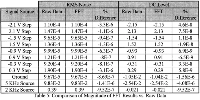
The final step in validating the accuracy of the 1/f noise test stations results is to verify the magnitude and frequency of the FFT results. To verify the magnitude of the results, all of the tests performed in this section were run with the debug flag described in Section 3.2.2 set. This left the last raw data set and results of the FFTs performed on it in memory at the end of the test. If the magnitude of the DC signal and the RMS noise calculated from both the FFT results and the raw
::::::::::::: :::: : : : : : :::::::: :::::::: : ..._ :::::::: ::: : ::: ::: :::::: : :::::::::::::::::: ::::: ::::::::: : : :::: : : : ::: ..._ :::: :: : ::: :::: :::: ::::::::::::::: : ::: :::::::::::::::: :::: :::: :::: ::::: : : :: : ::::: :: :: : : ::: 1::::::::::::: :: : :::: : : :: ::: :::::::::::::::::: :::::: : : ::::: : ::: :: *-i-i ii *iiiiiiiiiiiiiiiiiiiiiiiii:iiiiiii-:i-::::::: --- :: --- ---- :: : -- :' : : : ::: : : : : : : : : : : : ::: : :: : : : :: :: : ' :::::: : :::: : ::: :: :: :: -- : :-: -:- : :: ':-:-- : : :--: -: : : :':: : - : : :-: :- -- :--" '--- -::::::: :--::::- : ::-::::-:::::: -:::::':- ::: : ::'
data match, then all of the power from the raw data is being reflected in the FFT results. The power is not guaranteed to be in the proper frequency bin, but it is present.
Table 5 is a summary of the results from the all of the test performed in this section. During this test, the debug flag described in Section 3.2.2 was set. This table compares the DC signal level and RMS noise obtained from the output of the last averages FFT with that obtained from the raw data. In all cases, the percentage difference between the raw data and the FFT results is within 1E-6 percent. This is a good indication that the magnitude of the FFT results is very accurate.
-2.1 V Step 2.1 V Step -1.5 V Step 1.5 V Step -0.9 V Step 0.9 V Step -0.3 V Step 0.3 V Step Ground 5 KHz Source 2 KHz Source 1.10E-4 1.47E-4 9.65E-5 1.36E-4 9.99E-5 1.21E-4 9.20E-4 1.90E-4 9.67E-5 9.83E-2 0.39 1.10E-4 1.47E-4 9.65E-5 1.36E-4 9.99E-5 1.21E-4 9.20E-4 1.90E-4 9.67E-5 9.83E-2 0.39 -3.3E-6 -1.1E-6 -9.4E-7 -1.3E-6 -6.3E-7 -8E-7 -8.1E-7 -3.1E-6 -8.69E-7 -1.41E-6 -9.52E-7 -2.15 2.13 -1.54 1.52 -0.93 0.91 -0.31 0.29 -1.05E-2 -2.54E-2 -0.021 -2.15 2.13 -1.54 1.52 -0.93 0.91 -0.31 0.29 -1.04E-2 -2.54E-2 -0.021
Table 5: Comparison of Magnitude of FFT Results vs. Raw Data
4.6E-8 7.5E-8 1.1E-8 -1.9E-8 6.9E-9 -6.5E-9 3.3E-8 5.8E-9 -1.56E-6 -4.08E-6 -9.52E-7
The frequency accuracy of the system was verified by performing an FFT on a pure sine source with a known frequency. Two different sine sources were measured with both the 1/f noise test station and an Hewlett Packard 3561A spectrum analyzer. Both systems produced similar result for both frequency and magnitude. The 3561A is a calibrated piece of equipment and is sufficient to verify the performance of the station. Figure 8 shows the results of an FFT performed on a 5 KHz sine source.
Average FFT Data on 5 KHz 100 mV RMS Source 1.E+00 1.E-01 1.E-02 N . 1.E-03 1.E-04 1.E-05 1.E-06 0 5000 10000 15000 20000 Frequency
Figure 8: FFT of 5 KHz Sine Wave
4.1.2 Data Throughput
In terms of computational performance, the maximum data rate that the system could sustain real time calculations was measured to be 1.675 MHz. While this is fast enough to meet the requirements for this thesis, the value is significantly lower than the value estimated by the number
of clock cycles used by each portion of the program. Upon closer inspection, it was found that the transfer rate from the DAS to the HSDIO is currently limiting the performance of the system. Figure 9 shows an oscilloscope photo of the DAS interface's PCTL and PFLAG, as well as the HSDIO interface's External Write while the interface is operating at it's maximum speed. Note that all three of the signals in the picture are inverted. From the rising edge of PCTL (falling edge in picture) to the rising edge of PFLAG (falling edge in picture), it takes the DAS 400 ns to complete a read operation. It takes the HSDIO interface 200 ns to complete it's write operation (from rising edge of External Write to falling edge of External Write again inverted in photo).
For characterization purposes, DSP software was modified such that processor 0 no longer waited for the link port DMA to complete. Under these conditions, the system was able to perform FFTs on data coming in at 3.62 MHz, which is very close the predicted performance of the system.
'---PCTL
PFLAG
External write
Figure 9: Oscilloscope Photo of DAS to HSDIO Interface Operating at Maximum Speed
4.1.3 Overall Performance versus Thesis Goals
In addition to the verification tests as described in Section 4.1, this 1/f noise system was integrated into a production FPA test station. The 1/f noise system was able to perform the FFTs on the FPAs data at the rate that it was generated (1.4 MHz). This level of performance reduced test time by a factor of 20. Thus clearly the 1/f noise test station met or exceeded all of it's goals.
4.2 Potential Upgrades to the System
The system was designed with flexibility in mind. It should be useful for most FPA configurations with a minimum of work. The most beneficial upgrade to the system would be investigating the cause of the slow transfer rate from the DAS to the HSDIO interface. A simple change to the PLD could move the HSDIO write phase to very soon after PFLAG goes low. The data is available at this point, but it was decided that it should be given time to settle. This simple change would increase the interfaces data rate to 2.5 MHz. Any increase beyond this would involve modification to the DAS design. This should eventually be looked into.
Another optimization to the system that could make operate at much higher speeds is implementing the FIFO data overrun reset mentioned in section 3.2.1. This would make the system operate in a mode were it collected data then performed FFTs on it in serial. This trades significantly higher data rates for longer total test time.
The final optimization that should be considered is expanding the utilization of the system. A simple DSP program could be written that calculated average signal level and RMS noise on data acquired from the DAS. All current methods of doing this involve reading the data from the DAS into a host computer which does the necessary calculations. Unfortunately, getting data into the host computers is limited to a maximum of 500 KHz on all of the interfaces currently available to the computers used for testing. The DSP system has already proven that it could read data at much
higher rates. Using the system in this way would reduce test times for nearly every test station in use.
Bibliography
A.W. Drake, Fundamentals of Applied Probability Theory, New York, McGraw-Hill Book Company, 1967.
M. P. Niles, Reducing the Effects of l/f Noise in Infrared Imaging Systems, MIT Masters Thesis,
1991.
C. D. Motchenbacher, F. C. Fitchen, Low Noise Electronic Design, John Wiley & Sons, 1973
M. J, Buckingham, Noise in Electronic Devices and Systems, John Wiley & Sons, 1983
A. V. Oppenheim, R. W. Schafer, Digital Signal Processing, Prentice Hall Inc, 1975