Defect-Driven Processing of Two-Dimensional
Transition Metal Dichalcogenides
by
Kevin Christopher Bogaert
B.S. in Materials Science and Engineering Georgia Institute of Technology, 2014
Submitted to the Department of Materials Science and Engineering in Partial Fulfillment of the Requirements for the Degree of
Doctor of Philosophy
in Materials Science and Engineering at the Massachusetts Institute of Technology
June 2019
© 2019 Massachusetts Institute of Technology. All rights reserved.
Author: _______________________________________________________________________ Department of Materials Science and Engineering
April 30, 2019
Certified by: ___________________________________________________________________ Silvija Gradečak Professor of Materials Science and Engineering Thesis Supervisor
Accepted by: __________________________________________________________________ Donald R. Sadoway Chairman, Departmental Committee on Graduate Studies
3
Defect-Driven Processing of Two-Dimensional
Transition Metal Dichalcogenides
by Kevin C. Bogaert
Submitted to the Department of Materials Science and Engineering on April 30, 2019, in Partial Fulfillment of the
Requirements for the Degree of Doctor of Philosophy in Materials Science and Engineering
Abstract
Two-dimensional transition metal dichalcogenides (TMDs) are an emerging class of semiconductor materials that offer exciting new properties for future electronic and optoelectronic applications. However, many ongoing challenges related to synthesis and processing must be overcome before this nascent technology can become industrially viable. In this thesis, processing-related phenomena relevant to the fabrication of TMD heterostructures, alloys, and nanoporous membranes are presented.
This thesis begins with an investigation of the role of substrate temperature in two-step chemical vapor deposition (CVD) growth of MoS2/WS2 heterostructures. We demonstrate diffusion-mediated synthesis of inverted lateral heterostructures following low MoS2 growth temperatures in the second CVD step and homogeneous MoxW1-xS2 alloyed crystals following
higher MoS2 growth temperatures.
Investigating the nature of this diffusion-mediated process, we identify an energetically favorable atomistic model proposing that transition metal diffusion is driven by a heterogeneous distribution of sulfur vacancies. This model is corroborated by the synthesis of a composition-graded MoxW1-xS2 alloy crystals in which the final-stage spatial distribution of transition metal
4
atoms correlates with intermediate-stage distribution of point defects. These heterogeneous crystals allow for correlation of the local optical properties with the local composition,
demonstrating a variation in photoluminescence intensity spanning two orders of magnitude and reaching the maximum value for equicompositional alloy Mo0.5W0.5S2 (x=0.5).
Furthermore, the correlation between intermediate-stage distribution of point defects and final-stage spatial distribution of transition metal atoms enables the opportunity for bespoke patterning. Utilizing a laser annealing technique, we demonstrate the ability to locally induce defects that define the regions of preferential nucleation during subsequent CVD growth.
Finally, defect processing is also demonstrated in nanoporous TMD membrane applications. Combining modeling with experimentation, we demonstrate the relationship between vacuum annealing time and temperature with nanopore properties such as average radius and edge structure. Control of these properties is essential for the fabrication of functional nanoporous membrane devices for sensing, filtration, and energy applications.
This thesis motivates further work on TMD processing in pursuit of developing a fundamental understanding of the defect-driven diffusion mechanism, a larger library of interesting TMD compositions and structures, as well as industrially viable TMD devices.
Thesis Supervisor: Silvija Gradečak
5
Acknowledgements
I would like to thank my advisor, Prof. Silvija Gradečak. She provided a number of
opportunities for me to grow, professionally and personally, and supported me as the founding member of the two-dimensional materials branch of the lab. I would also like to thank Prof. Jeffrey Grossman and Prof. Carl Thompson for serving as members of my thesis committee and for offering support and advice throughout the course of this research.
I would also like to thank the current and former members of the Gradečak group. Jordan Chesin was an invaluable mentor to me during the early stages of my research, helping me to construct our first 2D materials CVD system and forming a journal club to stay up-to-date in the rapidly changing field of 2D research. Akshay Singh, Jian-An Ke, and Haeyeon Lee have spent countless hours working alongside me to improve growth recipes and develop various processing and characterization techniques. To the rest of the group – Hadi Dastjerdi, Sarah Goodman, Olivia Hentz, Zhibo Zhao, Nina Andrejevic, Jayce Cheng, Paul Rekemeyer, Sema Ermez, Eric Jones, John Hanson, and Denis Titow – for contributing technical expertise, listening to countless practice talks and research updates, sharing wisdom, and providing guidance and support.
I would also like to thank Prof. Slaven Garaj and the Garaj group at the National University of Singapore. Prof. Garaj hosted me as a visiting researcher in his lab four times for seven cumulative months, allowing me access to some of the most advanced equipment and leading experts in the field of 2D materials. My thesis would be an entirely different document if it were not for these opportunities. Over the course of my numerous visits to the Garaj group, I
developed meaningful research collaborations and friendships with members of the Garaj group. I would especially like to thank Song Liu, Tao Liu, Massimo Spina, Rajesh Sharma, and Milan Blašković. Also in the Singapore community, I would like to thank Prof. Chun Zhang and Na Guo of NUS for their DFT contributions to the work presented in Chapter 4 and Prof. Martial Duchamp and Chris Boothroyd of Nanyang Technological University for their TEM
contributions to the work presented in Chapter 6.
I would like to thank my friends and family for their support throughout this journey. I would like to thank Owen Morris, Jérôme Michon, Jonathan Hwang, and Seth Cazzell for the time we shared at our Seckel St. apartment as well as Erica Lai, Derek Kita, Chris Couch, and Jason Adams for their friendship and support. I owe an enormous debt of gratitude to Sarah Schwartz for providing the emotional support to help me savor the highs and survive the lows of graduate school. Lastly and most importantly, I am thankful for my parents, Debra and Paul, as well as my sister, Lauren, and my extended family for instilling the values and providing the never-ending support and love to help me pursue my dreams, wherever that journey takes me.
6
Table of Contents
List of Figures ... 8
List of Tables ... 14
List of Abbreviations ... 15
Chapter 1: Introduction and Motivation ... 17
1.1 Two-dimensional transition metal dichalcogenides... 18
1.1.1 Properties ... 18
1.1.2 Heterostructures ... 19
1.1.3 Alloys... 22
1.1.4 Defects... 23
1.2 Thesis outline ... 25
Chapter 2: Experimental Methods ... 29
2.1 Preparation of two-dimensional crystals ... 29
2.1.1 Mechanical exfoliation... 29
2.1.2 Chemical vapor deposition ... 32
2.1.3 Crystal transfer ... 45
2.2 Characterization techniques ... 49
2.2.1 Raman spectroscopy ... 50
2.2.2 Photoluminescence ... 55
2.2.3 Atomic force microscopy... 57
2.2.4 Scanning transmission electron microscopy ... 59
2.3 Conclusions ... 62
Chapter 3: Diffusion-Mediated Synthesis of MoS2/WS2 Heterostructures ... 63
3.1 Introduction ... 63
3.2 Results ... 65
3.2.1 Two-step growth process ... 65
3.2.2 Synthesis of phase segregated crystals ... 66
3.2.3 Synthesis of alloyed crystals ... 71
3.3 Conclusions ... 78
Chapter 4: Two-Dimensional MoxW1-xS2 Graded Alloys: Growth and Optical Properties 79 4.1 Introduction ... 79
4.2 Results ... 81
7
4.2.2 Correlating crystal defects with composition ... 82
4.2.3 Defect-driven synthesis of graded alloys ... 85
4.2.4 Correlating optical properties with composition ... 88
4.3 Conclusions ... 91
Chapter 5: Direct-Write Patterning of Two-Dimensional Heterostructures by Laser-Induced Defect-Engineering ... 93
5.1 Introduction ... 93
5.2 Results ... 96
5.2.1 Laser-induced local annealing ... 96
5.2.2 Location-controlled heterostructure formation ... 100
5.2.3 Laser power effects ... 105
5.3 Conclusions ... 107
Chapter 6: Nanopores in Transition Metal Dichalcogenides with Controlled Size and Edge Properties ... 109
6.1 Introduction ... 109
6.2 Results ... 111
6.2.1 Analytical modeling ... 111
6.2.2 Monte Carlo modeling ... 113
6.2.3 Microscopy experimental design ... 116
6.2.4 Nanopore edge structure ... 117
6.2.5 Nanopore growth rate ... 121
6.3 Conclusions ... 125
Chapter 7: Conclusions and Future Directions... 127
7.1 Conclusions ... 127
7.2 Recent advances and future directions ... 129
7.2.1 In situ observation of diffusion ... 129
7.2.2 Expanding the TMD library ... 130
7.2.3 Large-scale patterning of heterostructure and alloy devices ... 131
7.2.4 Device testing with processed TMD nanopores... 132
Appendix ... 135
8
List of Figures
Figure 1-1. (a) Planar and (b) side views of a MoS2 crystal. The red diamond in (a) defines the unit cell... 19 Figure 1-2. Schematics of a (a) vertical and (b) lateral heterostructure with 2D TMD domains. 20 Figure 1-3. Common point defects (top row) and grain boundary dislocations (bottom row) in
MoS2. ... 24 Figure 1-4. ZZ and AC edges of 2D TMDs. ... 25 Figure 2-1. (a) Ideal (i.e., log2(𝑚)) and (b) more realistic layer isolation pathways by
mechanical exfoliation. Mechanical exfoliation often results in a distribution of layer
numbers. ... 30 Figure 2-2. WS2 crystal example of the variety of crystal thicknesses achieved following
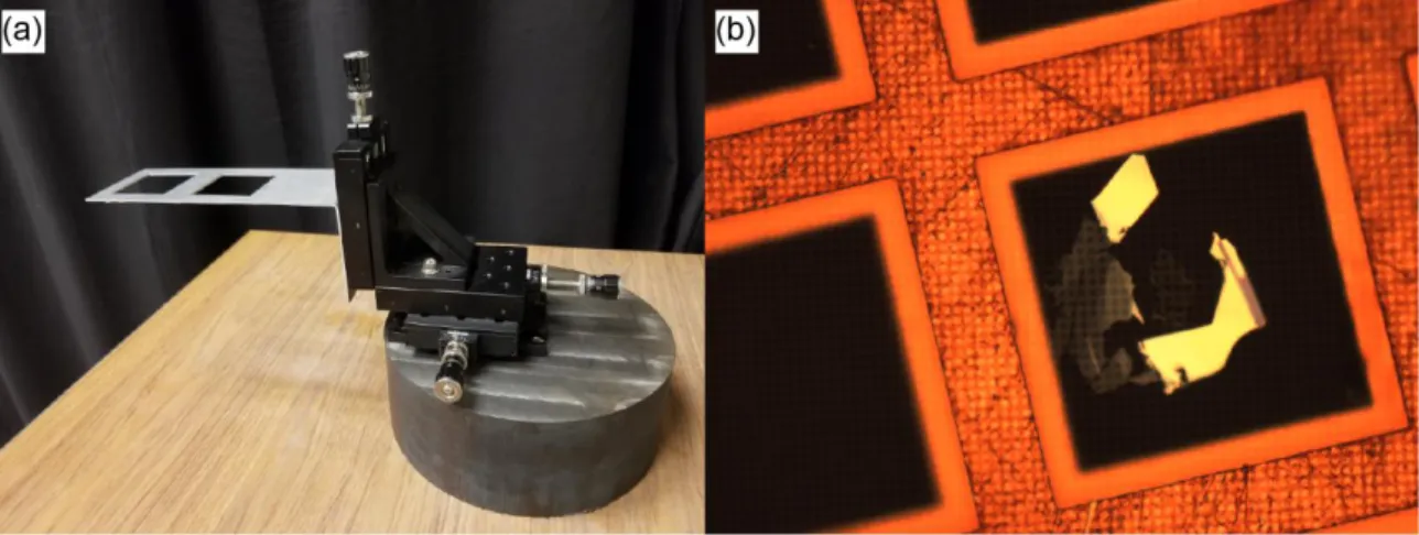
mechanical exfoliation ranging from monolayer (light purple, center) to few-layer (blue, upper left) to multi-layer (yellow, bottom and upper right). ... 31 Figure 2-3. Schematic of a typical CVD furnace set-up identifying the relative locations of key
components. ... 33 Figure 2-4. Gas flow regimes as a function of system dimensions and pressure. The approximate range of operating conditions reported throughout this thesis corresponds to the region within the grey rectangle in the viscous regime. Figure adapted from Ref. 99. ... 35 Figure 2-5. Schematics of (a) the stagnant film boundary layer, (b) concentration profile, and
fluxes. ... 36 Figure 2-6. Schematic of a three-zone CVD furnace set-up demonstrating the ability to achieve
thermal de-coupling of each precursor as well as the substrate. ... 37 Figure 2-7. Schematic plot of the temperature dependence of the growth velocity in different
growth regimes... 39 Figure 2-8. Energetics for calculating critical nucleation size and monolayer vs. multilayer
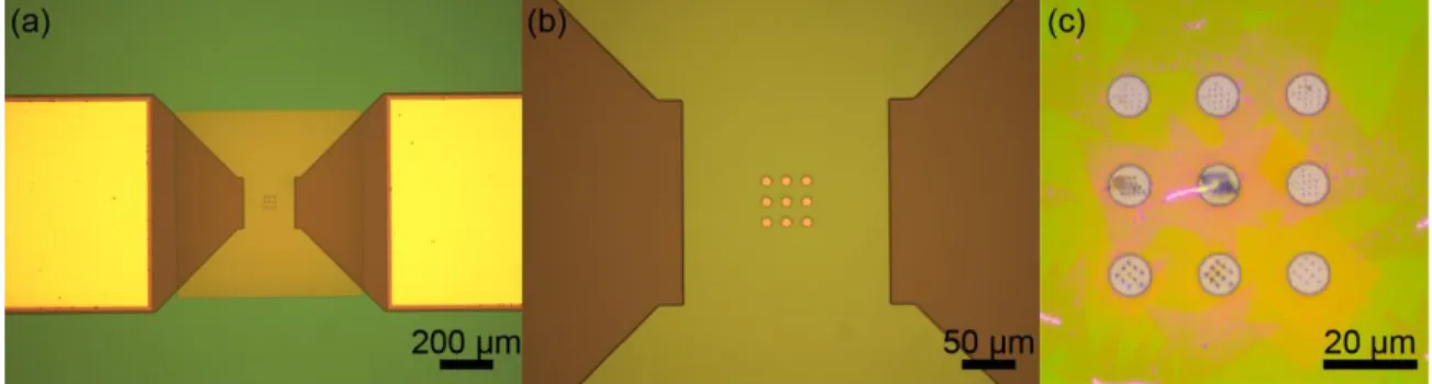
growth. Figure adapted from Ref. 32. ... 42 Figure 2-9. Schematic process of crystal transfer steps. ... 45 Figure 2-10. Photographs of (a) transfer step 1 (i.e., aligned placement of tape on the substrate)
and (b) transfer step 3 (i.e., aligned placement of crystal/tape structure on new TEM grid substrate). ... 46 Figure 2-11. (a) XYZ micromanipulator. (b) Crystal transferred onto Cu TEM grid with micron-scale precision. ... 48 Figure 2-12. Optical microscope images of Protochips Fusion in situ heating TEM grids with (a)
5×, (b) 20×, and (c) 100× objective lens magnification. MoS2 crystals are visible on the grid in (c) following the transfer technique described above. ... 49
9
Figure 2-13. (a) Schematic of vibrational energy state transitions involved in Raman scattering. (b) Schematic of relevant vibrational modes in MoS2. ... 50 Figure 2-14. Representative Raman spectra for pure monolayer MoS2 and WS2. The spectral
region of interest for most of the work presented in this thesis is defined by the grey
rectangle. ... 52 Figure 2-15. Evolution of Raman spectra in MoxW1-xS2 from x ≈ 1 (red) to x ≈ 0 (purple)... 53
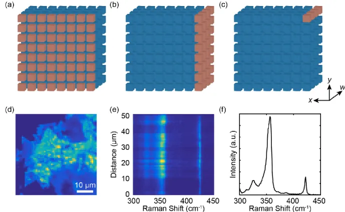
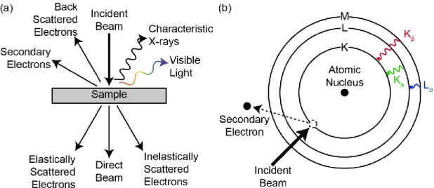
Figure 2-16. Methods of isolating components of a 3D data cube into (a) 𝑥-𝑦 maps at a given 𝑤, (b) 𝑥-𝑤 or 𝑦-𝑤 line scans at a given 𝑦 or 𝑥, respectively, or (c) individual spectra at a given (𝑥,𝑦) coordinate. Corresponding examples of a (d) map, (e) line scan, and (f) spectrum of a WS2 sample. ... 55 Figure 2-17. (a) Photoexcitation, (b) relaxation, (c) RR, and (d) SRH recombination. ... 57 Figure 2-18. Schematic of AFM measurement. ... 58 Figure 2-19. (a) Schematic representation of signals generated by electron beam irradiation.
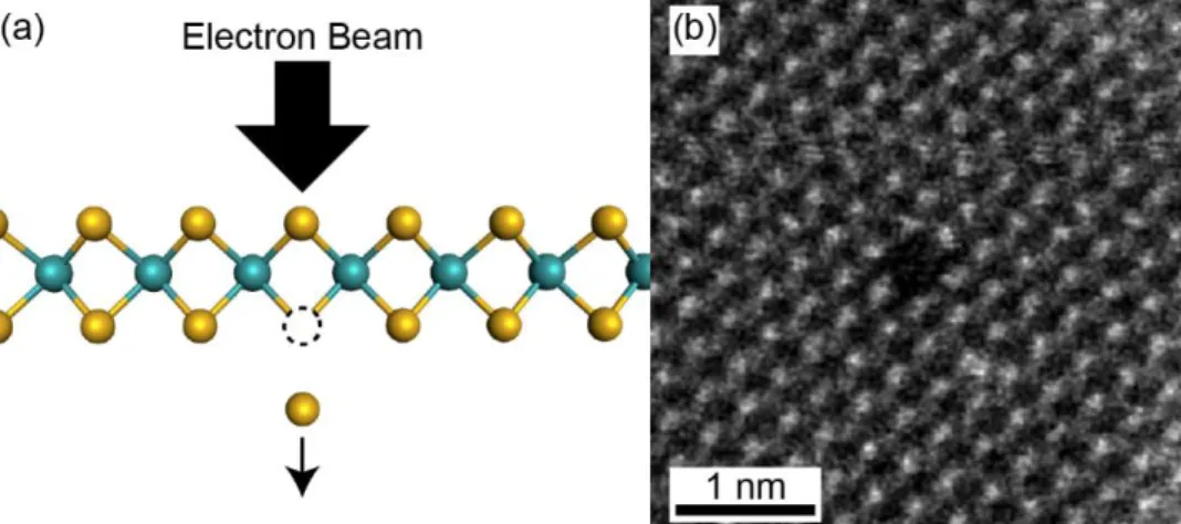
Adapted from Ref. 135. (b) Shell-to-shell transitions corresponding to the characteristic X-rays measured by EDS. ... 60 Figure 2-20. (a) Schematic of S ejection from electron beam energy transfer. (b) STEM image
of defective TMD lattice following electron beam-induced atomic ejection. ... 62 Figure 3-1. (a) Optical image of a WS2 crystal grown at 1100°C. (b) Raman spectra collected in
the points marked in Figure 3-1a. The dashed lines show the wavenumbers of the 𝐸2𝑔1 (~355 cm-1) and 𝐴1𝑔 (~420 cm-1) vibrational modes of WS2. ... 65 Figure 3-2. Proposed growth stages of MoS2/MoxW1-xS2 heterostructures (W atoms are green,
Mo atoms are red, S atoms are black). WS2 crystals are first grown at 1100°C (Stage I). MoS2 is then formed at the crystal edge after the growth temperature is reduced and MoO3 is introduced into the growth chamber (Stage II). Depending on the substrate growth
temperature during the MoS2 growth step, the crystal forms either a phase-segregated heterostructure with a Mo-core at low temperatures (Stage III-L) or a near-uniform Mox W1-xS2 alloy at high temperatures (Stage III-H). ... 66
Figure 3-3. (a) Optical, (b) AFM, and (c) SEM secondary electron images of a typical
heterostructure grown at 𝑇𝐺(2) = 650°C (Stage III-L). Scale bar in (a) applies to (a-c). (d) EDS map of a Stage III-L crystal. Yellow and purple correspond to W and Mo, respectively. Colored circles correspond to the locations of EDS spectra in (e). (e) EDS spectra of the ring (blue) and core (green). ... 67 Figure 3-4. Raman intensity maps of the 𝐸2𝑔1 vibrational modes associated with (a) MoS2, (b)
WS2, and (c) W-rich MoxW1-xS2 alloys. Scale bar in (a) applies to (a-c). (d) Raman intensity
line scan corresponding to dashed line in (b). (e) HAADF STEM image of the domain interface... 69 Figure 3-5. (a) Composite Raman intensity map of the W-rich Mo1-xWxS2 core domain (~373
cm-1, yellow) and WS2 ring domain (~355 cm-1, blue). (b) Raman intensity line scan corresponding to dashed line in (a). (c) Contact potential difference mapping of the lateral
10
heterostructure, demonstrating an abrupt interface. The high intensity region in the upper left corner is due to residual PMMA from crystal transfer and should not be considered as a meaningful feature. ... 70 Figure 3-6. Raman intensity maps of the (a-d) MoS2 and (b-h) WS2 𝐸2𝑔1 vibrational modes
and (i-l) corresponding composite images from the Raman intensity maps indicating the relative positions of MoS2 (cyan) core and WS2 (red) ring domains. ... 71 Figure 3-7. (a) Optical, (b) AFM phase, (c) PL intensity, and (d) PL peak wavelength imaging
of a representative alloy crystal grown at 𝑇𝐺(2) = 680°C (Stage III-H). (e) STEM image of a Stage III-H crystal. Colored circles correspond to the locations of EDS spectra in (f). Scale bar in (a) applies to (a-e). (f) EDS spectra of the crystal edge (blue) and interior (green). .... 73 Figure 3-8. Raman intensity maps of the (a) MoS2 and (b) WS2 𝐸2𝑔1 vibrational modes. (c)
Raman intensity line scan corresponding to dashed line in (b). ... 74 Figure 3-9. Additional examples of PL (a-d) intensity and (e-h) peak position fluctuations in
nearly uniform MoxW1-xS2 alloy crystals. ... 75
Figure 3-10. (a, d) Optical image and Raman intensity maps corresponding to the 𝐸2𝑔1 modes of (b, e) WS2 and (c, f) MoS2. Results are shown following (a-c) WS2 growth and (d-f) subsequent 710°C MoS2 growth. WS2 remains present throughout the crystal following the MoS2 growth step. However, the MoS2 Raman map indicates the inter-diffusion of Mo atoms into the TMD lattice. AFM cross-sectional contour plots in (a) and (d) show the height of the crystal to be 2.5 nm after the first and second growth. ... 76 Figure 3-11. (a) Optical image of a thicker lateral heterostructure after the second MoS2 growth
at 710°C. Raman intensity maps of the 𝐸2𝑔1 mode of (b) MoS2 and (c) WS2. MoS2 is initially deposited at the activated WS2 edge area, described in Stage II in Figure 3-2. The lack of inter-diffusion could be attributable to factors such as insufficient growth time or the crystal thickness. ... 76 Figure 4-1. Raman position of the 𝐴1𝑔 vibrational mode for (a) exfoliated WS2 (yellow)
followed by grown MoS2 (cyan) and (b) exfoliated MoS2 (cyan) followed by CVD-grown WS2 (yellow). Both growths result in a lateral heterostructure with a sharp interface and chronological core-shell configuration indicating that no significant amount of diffusion occurred... 82 Figure 4-2. Monolayer WS2 crystal configuration used for DFT calculations. The crystal
contains one S vacancy (orange) and one Mo adatom (purple). ... 83 Figure 4-3. DFT-calculated proposed reaction path and schematics of atomic configurations for
inward diffusion of a Mo atom and outward diffusion of a W atom and S vacancy. From the Initial Stage to Stage 2, a Mo adatom and S atom diffuse inward together, resulting in the outward diffusion of a S vacancy. From Stage 2 to the Final Stage, the Mo adatom
incorporates into the metal plane of atoms, displacing a W atom, which then diffuses outward through the S vacancy site to the crystal edge. This reaction is exothermic. ... 85 Figure 4-4. Averaged Raman spectrum of a WS2 crystal grown using NaCl. Inset maps the ratio
11
graded distribution of defects within the crystal with the highest concentration in the center. ... 86 Figure 4-5. (a) Raman position of the 𝐴1𝑔 vibrational mode (and thus the composition x) of a
MoxW1-xS2 graded alloy crystal. (b) Corresponding PL peak energy map. (c) Crystal
composition as a function of the position along the arrow shown in (a) determined using the Raman 𝐴1𝑔 vibrational mode. The line is a guide for eye. ... 87 Figure 4-6. (a, d) Raman position maps of the 𝐴1𝑔 vibrational mode, (b, e) PL peak energy
maps, and (c, f) Raman line scans corresponding to the dashed lines in (a) and (d),
respectively, of additional MoxW1-xS2 graded alloy crystals. ... 88
Figure 4-7. Heat map correlating the Raman position of the 𝐴1𝑔 vibrational mode and the PL peak energy from a single MoxW1-xS2 graded alloy crystal, using the data represented in
Figure 4-5a and b, respectively. ... 89 Figure 4-8. (a) Normalized PL spectral evolution from the crystal core (cyan, left-most
spectrum) toward the edge (red, right-most spectrum). (b) Spatial map of the PL intensity within the crystal shown in Figure 4-5, plotted on a log scale. (c) Color-coded map of the crystal indicates PL data points extracted for the unstrained (blue) and strained (red) regions, as shown in (d). From the crystal center, all pixels of the crystal within 1.5 degrees of the symmetry lines connecting the center to the corner are colored red, indicating regions of greatest strain. All pixels greater than 6 degrees away from the symmetry lines are colored blue, indicating regions of least strain. (d) PL peak energy vs. intensity of the graded alloy crystal. Top scale shows the corresponding composition x determined from Raman
measurements (we note that the scale is not linear due to non-linear relation between the PL peak energy and the composition). The blue(red) data points in the graph were taken from the blue(red) (i.e., unstrained(strained)) regions of (c). Dashed line is a guide for eye for the unstrained data, which mostly follows the average value of the blue data points. ... 91 Figure 5-1. (a, c, e) Schematic and (b, d, e) proof-of-concept example of three-step
heterostructure formation process. (a, b) An initial TMD crystal is identified on a flat substrate. (c, d) Laser exposure results in thermally induced defect formation. (e, f) TMD growth preferentially occurs at the previously exposed location. ... 95 Figure 5-2. Raman mapping of the 𝐴1𝑔 vibrational mode in MoS2 crystals (a) before and (b)
after 532 nm laser annealing. (c) SEM image of the same crystal after laser annealing and (d) a higher magnification SEM image corresponding to the area indicated by the yellow dashed rectangle in (c). Scale bar in (a) applies to (a-c). ... 97 Figure 5-3. (a, b) Optical microscopy, (c, d) PL intensity, (e, f) Raman WS2 E2g1 intensity, (g,
h) AFM height, and (i, j) AFM phase images of a WS2 crystal before (left) and after (right) laser exposure. Laser exposure lines for 785, 633, and 532 nm are marked in (j) by red, yellow, and green arrows, respectively. The location of Figure 5-6 is marked in (l) by the yellow dashed square. (k, l) SEM image of the same crystal after laser annealing. The
location of (l) is indicated by the yellow dashed square in (k). Scale bar in (a) applies to (a-k). ... 99 Figure 5-4. (a, b) HAADF STEM image of laser annealed WS2. EDS mapping of (c) W and (d)
12
Figure 5-5. Raman intensities maps of (a) WS2 𝐸2𝑔1 and (b) MoS2 𝐴1𝑔 vibrational modes corresponding to the region of interest indicated in Figure 5-3j indicated by the yellow dashed square. (c) AFM height map and (inset) representative height profile demonstrating the height difference between the initial WS2 crystal and the newly grown MoS2 patterned region. (d) Average Raman spectra of regions marked by the dashed rectangles in (b). ... 101 Figure 5-6. Raman mapping of (a) WS2 𝐸2𝑔1 and (b) MoS2 𝐴1𝑔 vibrational mode intensities
corresponding to the region of interest in Figure 5-1f following 532 nm laser annealing and MoS2 growth. The MoS2 intensity is stronger and the WS2 intensity is weaker along the exposed line that was laser annealed. (c) Averaged Raman spectra of the regions marked by the dashed rectangles in (b). Red corresponds to the the spectra of the laser annealed line and cyan corresponds to an unexposed region. The MoS2-like vibrational mode intensities at approximately 385 and 403 cm-1 are stronger in the red spectrum, whereas the WS2-like vibrational mode intensities at approximately 355 and 420 cm-1 are stronger in the cyan spectrum. ... 102 Figure 5-7. (a-c) Optical microscopy and (d-f) Raman mapping at each of the three processing
stages of defect-driven heterostructure formation. Both laser annealing lines were formed using a 633 nm laser. Raman intensity in (d, e) correspond to the WS2 𝐸2𝑔1 vibrational mode. Raman intensity in (f) is gray-scale for the WS2 𝐸2𝑔1 mode and red for the MoS2 𝐴1𝑔 mode. The scale bar in (a) corresponds to (a-f). (g) AFM phase and (h) height mapping following laser annealing and (i) height mapping following MoS2 growth. Scale bar in (g) applies to (g-i). ... 103 Figure 5-8. (a-c) Optical microscopy at each of the three processing stages. Raman mapping of
the final crystal at the (d) MoS2 and (e) WS2 𝐸2𝑔1 vibrational modes. Colored arrows in (e) correspond to the laser wavelengths used to anneal each of the three lines. (f) A composite image of (d, e) with the MoS2 intensity represented in red and the WS2 intensity represented in cyan. (g) PL map following laser annealing. (h) AFM height map following MoS2 growth. (i) SEM image following laser annealing. (j) Averaged Raman spectra corresponding to a 633 nm laser annealed line (red) and region of unexposed WS2 crystal (cyan) indicated by dashed rectangles in (d). The laser annealed region indicates higher Raman intensities corresponding to MoS2 and the unexposed region indicates higher Raman intensities
corresponding to WS2. All scale bars are 5 µm. Scale bar in (a) applies to (a-c). Scale bar in (d) applies to (d-f). ... 105 Figure 5-9. (a) Optical microscopy of WS2 following laser annealing. The black and white
arrows mark the laser-patterned lines using 4.625 and 9.29 mW laser powers, respectively. (b) AFM height map following patterned growth of MoS2. (c) Average Raman spectra of regions marked in (a) by the dashed rectangles. The green and blue spectra containing both MoS2 and WS2 vibrational mode intensity peaks correspond to regions with high- and low-power laser exposure, respectively, while the red spectrum containing only WS2 vibrational mode intensity peaks corresponds to an unexposed region. ... 106 Figure 6-1. Initial state of nanopore growth with one disulfur vacancy (𝑉𝑆2) and three edge Mo
atoms. ... 112 Figure 6-2. (a, b) Monte Carlo simulations of the pore perimeter, area, and morphology
13
(a, c) correspond to the iteration step when the atomic column becomes fully removed. Pore area demonstrates less statistical noise, making it a more reliable metric for pore growth. Removal probability has a positive correlation with extent of faceting. ... 114 Figure 6-3. (a) Radial growth rate G𝑅 and faceting parameter fp as a function of removal
probability pr. (b) The distribution of rough and faceted edges in the final configuration of Monte Carlo simulated nanopores as a function of removal probability. The solid lines and shaded regions represent the average and standard deviation of 30 simulations at each probability. Probability values are in increments of 0.05 in the range 𝑝𝑟 = 0.6 − 0.8 and in increments of 0.01 in the range 𝑝𝑟 = 0.8 − 1. (c) Log-log plot of the results shown in (a) such that the x-axis is linearly proportional to inverse temperature showing the Arrhenius behavior... 115 Figure 6-4. (a) Fourier filtered and contrast adjusted STEM image of nanopores in MoS2. (b)
Binary image of nanopore objects identified by built-in MATLAB Image Segmenter app. (c) Comparison of original STEM image and overlaid nanopore objects identified. ... 117 Figure 6-5. Room temperature HAADF STEM images of MoS2 nanopores annealed at (a)
400°C for 6 min and (b) 700°C for 3 min. The bright dots correspond to Mo atoms and the fainter dots correspond to pairs of S atoms. Large high-intensity areas at the pore edges are comprised of Mo and/or S atoms that have been displaced out of the monolayer crystal lattice. Klein and ZZ edges are predominantly present in (b). (c) Schematic of Mo-terminated hexagonal pore faceting demonstrated in (b). Cyan corresponds to Mo and yellow corresponds to S. ... 118 Figure 6-6. MoS2 nanopores following annealing at 400, 450, 500, 600, and 700°C. ... 119 Figure 6-7. WSe2 nanopores following annealing at 400, 500, 600, and 700°C. Images at 500
and 600°C show stability of both the ZZ and AC edge orientations. ... 119 Figure 6-8. MoxW1-xS2 (x ≈ 0.1) nanopores following annealing at 700 and 750°C. ... 120
Figure 6-9. (a) High magnification STEM image of MoS2 nanopore shown in Figure 6-5b. (b-d) Higher magnification images corresponding to colored dashed rectangles in (a)
demonstrating (b, d) Mo-Klein and (c) Mo-ZZ edges. ... 121 Figure 6-10. (a-c) A representative set of HAADF STEM images of a single nanopore in MoS2
as a function of the annealing time (indicated in the images) at 450°C. (d) Average radii of seven different nanopores (shown in different colors) of different initial sizes as a function of annealing time at 450°C. (e) Radial growth rate 𝐺𝑅 is independent of pore radius 𝑟. Dashed line represents the average growth rate and shaded region represents the standard deviation. ... 123 Figure 6-11. Combined data sets and corresponding quadratic fits of MoS2 nanopore area as a
function of annealing time at (a) 450 and 500°C, (b) 600°C, and (c) 700°C. Each marker color corresponds to a different pore. (d) Arrhenius plot of the linear fitting coefficients in (a-c) as a function of annealing temperature. The exponential coefficient of the fitted Arrhenius equation is proportional to the activation energy of nanopore growth. ... 125
14
List of Tables
Table 1-1. Optical band gaps and lattice constants of some of the most commonly studied monolayer TMDs.24–26 ... 19
15
List of Abbreviations
Abbreviations
2D Two-dimensional
AC Armchair
AFM Atomic force microscopy
CVD Chemical vapor deposition
DNA Deoxyribonucleic acid
DFT Density functional theory
EDS Energy-dispersive X-ray spectroscopy HAADF High-angle annular dark field
IQE Internal quantum efficiency
NR Non-radiative
PL Photoluminescence
PMMA Poly(methyl methacrylate)
RPM Rotations per minute
RR Radiative recombination
SEM Scanning electron microscopy
SRH Shockley-Read-Hall
STEM Scanning transmission electron microscopy TEM Transmission electron microscopy/microscope TMD Transition metal dichalcogenide
vdW van der Waals
16 Mathematical symbols
𝑎 Interatomic distance
𝛼 Average surface area per atom
𝐴 Area
𝐶 Concentration
𝑑𝑆𝐹 stagnant film boundary layer thickness
𝐷 Diffusivity 𝐸𝑎 Activation energy 𝑓𝑃 Faceting parameter 𝐹 Flux 𝛾 Surface energy 𝐺 Free energy
𝐺𝑅 Average radial growth rate
Γ Jumping rate
ℎ𝐺 Gas phase mass transport coefficient ℎ𝑉𝑎𝑝 Enthalpy of vaporization
𝑘𝐵 Boltzmann constant
𝑘𝑆 Surface reaction rate constant
𝜆 Mean free path
𝑚 Layer number
𝜇 Viscosity
𝑛 Number of clusters
𝜈 Jumping attempt frequency
𝑁 Number of atoms 𝑝𝑅 Removal probability 𝑃 Pressure 𝑟 Radius 𝜌 Density 𝑅𝑒 Evaporation rate 𝑡 Time 𝜏 Carrier lifetime 𝑇 Temperature
𝑈 Bulk gas flow velocity
𝑤 Wave number
𝑥 Spatial distance or alloy composition
𝑦 Spatial distance
17
Chapter 1: Introduction and Motivation
The 1956 Nobel Prize in Physics was awarded to William Shockley, John Bardeen, and Walter Brattain “for their researches on semiconductors and their discovery of the transistor effect.”1 Their 1947 invention of a working solid-state transistor demonstrated a scalable
replacement to the vacuum tube technology used in early computing. Over the following decades to the present day, advances in semiconductor research and transistor manufacturing for the computing industry have followed a trend known as Moore’s Law, resulting in an approximately biennial doubling in the number of components per integrated circuit.2
Alongside these advances in computing technologies, other semiconductor technologies such as photovoltaics3 and light emitting diodes4 have improved significantly due to research in materials discovery and processing. In addition to the thorough understanding of silicon-based technologies built on over a half-century of research, semiconductor device prospects have also significantly improved due to research in alternative semiconducting materials such as III-V,4 carbon nanotube,5 perovskite,6 and two-dimensional (2D) materials.7,8 These alternative semiconducting materials have the potential to enable further advancement in device performance for various applications in which their unique properties exceed those of more traditional options such as silicon. To achieve this potential, these materials must escape their relative nascence to become well-understood technologies with processing capabilities and control on par with competitive traditional devices.
In this chapter, we will introduce two-dimensional transition metal dichalcogenides (TMDs) as an emerging class of semiconducting materials. By discussing the novel properties and
18
the work discussed in the remainder of this thesis which aims to address some of these challenges.
1.1 Two-dimensional transition metal dichalcogenides
1.1.1 Properties
TMDs such as MoS2 are naturally occurring crystalline minerals. The crystal structure consists of three-atom-thick sheets (i.e., monolayers) with a hexagonal atomic arrangement (Figure 1-1).9 The hexagonal lattice consists of alternating sites of either a single transition metal atom (e.g., Mo, W) or a pair of chalcogen atoms (e.g., S, Se, Te). The transition metal atom is positioned in the central plane of the sheet whereas the pair of chalcogen atoms are split into the top and bottom planes. Ideal monolayers have no c-axis dangling chemical bonds and are only bound to their substrate or other TMD monolayers by van der Waals (vdW) bonding with a layer thickness of approximately 6.5 Å.
Due to the weak nature of vdW bonding, bulk TMDs have commonly been used as dry lubricants alongside graphite, another vdW-bonded layered material.10,11 In 2004, monolayers of graphite (i.e., graphene) were isolated and measured to be semimetals with a strong ambipolar electric field effect and room-temperature mobilities of ~10,000 cm2/Vs.12 For their isolation and characterization of graphene as a remarkable 2D conductor, Andre Geim and Konstantin
Novoselov were awarded the 2010 Nobel Prize in Physics.13 In that same year, the isolation of monolayer MoS2 was first reported. Early research on monolayer MoS2 demonstrated quantum confinement effects upon thinning to the monolayer limit such as a crossover from an indirect band gap to direct band gap and a consequent improvement in luminescence quantum yield by orders of magnitude.14–16 Shortly thereafter, MoS2 field-effect transistors were reported with a room-temperature current on/off ratio exceeding 1×10⁸ and mobility of ~200 cm2V-1s-1.17 With
19
direct band gap energies ranging from 1.55 to 1.97 eV (Table 1-1) and exciton binding energies of 320 to 570 meV,18–20 monolayer TMDs are a promising class of materials for high-speed and low-power electronic, optoelectronic and photonic applications.21–23
Figure 1-1. (a) Planar and (b) side views of a MoS2 crystal. The red diamond in (a) defines the unit cell.
Material Band Gap (eV) Lattice Constant (Å)
MoS2 1.82 3.160
WS2 1.97 3.155
MoSe2 1.55 3.299
WSe2 1.65 3.286
Table 1-1. Optical band gaps and lattice constants of some of the most commonly studied monolayer TMDs.24–26
1.1.2 Heterostructures
Due to the composition-dependent properties of 2D TMDs, there is a desire to create
20
material properties, such as a p-n junction. These 2D heterostructures are divided into two classes by the topology of their interfaces: lateral and vertical heterostructures (Figure 1-2).24 In a lateral heterostructure, the full structure is a single monolayer in which the composition of the monolayer varies in-plane. Consequently, the interface between the constituent materials is one-dimensional and comprised of chemical bonds. In a vertical heterostructure, the full structure is comprised of multiple monolayers stacked on top of one another in which the constituent materials occupy separate planes. Vertical heterostructure interfaces are two-dimensional and comprised of vdW bonds.
Figure 1-2. Schematics of a (a) vertical and (b) lateral heterostructure with 2D TMD domains. As indicated in Table 1-1, the lattice constants of TMDs sharing the same chalcogen element are virtually identical whereas the lattice constants of TMDs with different chalcogen elements vary by a few percent. Given that TMDs also share the same hexagonal monolayer crystal structure, it is relatively trivial to construct high-quality interfaces between these materials to form heterostructures, albeit with some strain or dislocations in the case of lateral
heterostructures with different chalcogen elements.
Vertical heterostructures can be synthesized by mechanical stacking techniques (see Section 2.1.1) or by chemical growth techniques (see Section 2.1.2) due to the poor bonding between layers. However, the in-plane chemical bonding within monolayers necessitates that lateral
21
heterostructures must be produced by chemical growth techniques. Lattice continuity of lateral heterostructures yields superior in-plane electronic properties, including excellent current rectification behavior and photocurrent generation characteristics.27,28 Furthermore, lateral in-plane heterostructures can act as intrinsic p-n junctions and have arbitrarily tuned bandgaps via alloying. Chemical growth presents a more scalable and reproducible method for heterostructure fabrication and so it has generated more interest within the field. Several chalcogen-changing (e.g., MoS2/MoSe2 or WS2/WSe2), metal-changing (e.g., MoS2/WS2 or MoSe2/WSe2), and dual-changing (e.g., MoS2/WSe2) lateral heterostructures grown by chemical vapor deposition (CVD) have been reported.24,27–34
In one-step lateral heterostructure growth processes, two metallic precursors are
simultaneously present in the reaction chamber during the growth; after the growth, the material with higher vapor pressure and nucleation rate is found in the core of the 2D crystal.24,29,31,34–38 In two-step growths, the core domain of the first material is grown first, followed by the exchange of precursors and the growth of the ring of the second material.27,28,30,32,39 While these growth techniques are successful, they offer little control for complexity as the radial domain
configuration is strictly a function of growth chronology.
One of the goals of the work presented in this thesis is to develop an understanding of the mechanisms that govern the growth of pure and multi-phase TMDs that will be critical for engineering more advanced heterostructures with controlled properties. This involves an investigation of the role of processing parameters, as will be discussed in Chapter 3, as well as the development of new processing techniques, as will be discussed in Chapter 5.
In addition to the work presented in this thesis, other researchers have made parallel developments in the field of 2D TMD processing. These include top-down patterning methods
22
involving masked etching,40,41 selective chalcogen conversion of MoSe2 into MoS2/MoSe2 heterostructures,42 and bottom-up methods of surface functionalization and lithographically patterned seeding to yield selective nucleation.43–47 While these techniques have provided useful contributions to the field, further research is still necessary to enable the fabrication of arbitrary heterostructures with highly controlled spatial configurations of domains with bespoke
compositions and properties. 1.1.3 Alloys
In addition to the benefits of creating atomically abrupt hetero-interfaces, there are also benefits to creating 2D TMD alloys by utilizing the similar crystal structure and lattice spacing of these materials to create crystals that possess properties that continuously span the full range of their pure counterparts. These alloyed crystals can be divided into multiple classes based on composition (i.e., metal-alloyed and/or chalcogen-alloyed) or spatial distribution (i.e., uniform or graded). Similar to one-step lateral heterostructure growth processes, composition-graded alloy growth processes often involve the delayed introduction and/or vaporization of one or more precursor, resulting in a radial composition distribution that correlates with the chronology and relative abundance of each precursor.34–36,48–51 Conversely, uniform alloy growth processes aim to maintain a constant abundance of each precursor throughout crystal growth.52–59 Beyond alloying by growth, alloying can also be achieved by post-processing of crystals through techniques such as atomic substitution.60 As with heterostructures, there is an ongoing need to improve the processing capabilities and controls of TMD alloys to enable the fabrication of crystals with high spatial control of local composition and properties, as will be discussed in Chapter 4.
23 1.1.4 Defects
Like in any other crystalline solid, defects are thermodynamically inevitable in monolayer TMDs. Limited by the dimensionality of the crystal, defects in 2D TMDs exist in no greater than two dimensions of space. Examples of common structural defects in TMDs include 2D pores,61 1D dislocations and grain boundaries,62,63 and 0D point defects (e.g., substitutions, vacancies) (Figure 1-3).64
Vacancies are especially common in chemically grown samples due to imperfections in the growth process. Monosulfur vacancies (𝑉𝑆) have the lowest formation energy among the intrinsic point defects in monolayer MoS2, followed by disulfur vacancies (𝑉𝑆2), molybdenum vacancies
(𝑉𝑀𝑜), vacancy complexes (e.g., 𝑉𝑀𝑜𝑆3), and eventually antisite defects (e.g., 𝑀𝑜𝑆2 or 𝑆2𝑀𝑜).
64
Although a non-zero concentration of monosulfur vacancies is expected to exist, an excess of vacancies beyond thermodynamic equilibrium can exist due to external factors such as sample irradiation or annealing. Under high vacancy conditions, material systems are subjected to a thermodynamic driving force to minimize the energy of the system by vacancy agglomeration. In monolayer transition metal disulfides, this has been observed to occur by a process of sulfur vacancy diffusion into 1D vacancy channels.65–68
24
Figure 1-3. Common point defects (top row) and grain boundary dislocations (bottom row) in MoS2.64
Two-dimensional pores in TMDs are often the result of thermal decomposition and/or oxidation.61,69,70 This process can be initiated during chemical growth due to a precursor
deficiency, following growth due to aging in air, or during post-growth processing steps. While crystalline defects are typically considered undesirable, controllable fabrication of nanometer-scale pores in 2D TMDs are highly desirable for energy, filtration, and sensing applications, as will be described in greater detail in Chapter 6. Due to the hexagonal nature of the TMD crystal structure, nanopores in TMDs often tend to possess 3-fold or 6-fold symmetries, terminated by low-index facets such as the zigzag (ZZ) or armchair (AC) edges (Figure 1-4).
25 Figure 1-4. ZZ and AC edges of 2D TMDs.
1.2 Thesis outline
In this thesis, we explore the effects of defect-driven processing of 2D TMD semiconducting materials. We first demonstrate how the control of substrate temperature in CVD can allow for diffusion-mediated synthesis of heterostructures and alloys in 2D TMDs. We then determine the scope of this diffusion-mediated process by identifying a defect-driven atomistic model that is corroborated by our synthesis of chemically-graded alloys in which the composition is
determined by the defect distribution. Next, we expand the control of defect placement by developing a laser-based technique for direct-write defect patterning that translates into bespoke heterostructure patterning. Finally, we investigate the application of 2D TMD defect processing to the field of nanoporous membrane technology.
Chapter 2 introduces the experimental methods used in this thesis, focusing on sample preparation and characterization. Sample preparation includes 2D TMD crystal isolation by mechanical exfoliation, crystal growth by chemical vapor deposition, and methods of crystal transfer from native SiO2 substrates to transmission electron microscopy (TEM) grids. Sample characterization includes a variety of techniques utilizing lasers, scanning probes, and electron
26
beams to map the local properties of these samples. The techniques of Raman spectroscopy, photoluminescence (PL) spectroscopy, atomic force microscopy (AFM), and scanning
transmission electron microscopy (STEM) will form the basis of our experimental investigation and will therefore be discussed in detail.
Chapter 3 investigates how substrate temperature in the second step of a two-step CVD process affects compositional configuration in the (Mo/W)S2 material system. Lateral heterostructures of MoS2-WS2 and alloys of MoxW1-xS2 are presented following otherwise
comparable CVD procedures. We present Raman and PL spectroscopy characterization of the composition as a function of position. We propose a diffusion-mediated process to explain the observations.
Chapter 4 continues the investigation of the nature of the proposed diffusion-mediated process. By replacing the first CVD step of the two-step process with mechanical exfoliation of either MoS2 or WS2, we investigate the limitations of the diffusion-mediated process in an attempt to understand the mechanism. We present an energetically favorable atomistic model proposing that the transition metal diffusion process is driven by a heterogeneous distribution of point defects. This model is corroborated by the synthesis of a composition-graded MoxW1-xS2
alloy in which the final-stage spatial distribution of transition metal atoms correlates with intermediate-stage distribution of point defects. Additionally, we analyze the spatially
heterogeneous PL spectra of these graded alloy crystals to correlate local optical properties with the local composition.
Chapter 5 investigates methods of controlling the intermediate-stage distribution of point defects to enable direct-write defect patterning that translates into bespoke heterostructure patterning. Utilizing a laser annealing technique, we demonstrate the ability to locally induce
27
defects. These defects serve as preferred sites for heterostructure formation during subsequent CVD growth. Using this technique, we are able to create arbitrarily patterned MoS2-WS2 heterostructures.
In Chapter 6, we turn our attention to defect processing for nanoporous 2D TMD membrane applications. We present series of atomically resolved STEM images of nanoporous 2D TMDs throughout intermittent in situ vacuum annealing. We examine both the evolution of the
nanopore edge structure as well as the rate of growth as functions of annealing temperature. We corroborate these experimental findings with Monte Carlo modeling and the presentation of a fundamental mathematical framework.
Finally, in Chapter 7 we will conclude this thesis by summarizing the important scientific contributions of this work and suggesting future directions of research in this field based on the results presented here.
29
Chapter 2: Experimental Methods
The experimental work presented throughout this thesis can be divided into two classes: sample synthesis/preparation and sample measurement. The first section of this chapter focuses on various methods of sample preparation including the simple top-down method of isolating TMD monolayers by mechanical exfoliation and the more versatile bottom-up method of growing crystals by CVD. The advantages, disadvantages, and important considerations of each of these techniques will be discussed. The ability to transfer crystals from their native substrate to new substrates is critical to enable investigation by TEM. Best known practices and important considerations for crystal transfer will be discussed. The second section of this chapter focuses on various methods of sample measurement utilizing lasers, scanning probes, and electron beams to map the local properties of these samples. The techniques of Raman spectroscopy, PL spectroscopy, AFM, and STEM will form the basis of our experimental investigation and will therefore be discussed in detail.
2.1 Preparation of two-dimensional crystals
2.1.1 Mechanical exfoliation
The fundamental principle of mechanical exfoliation of layered materials such as TMDs is the utilization of weak inter-layer vdW bonds to separate layers from each other. In an ideal scenario, a single crystal containing 𝑚 layers can be divided into two equal parts log2𝑚 times to produce 𝑚 separate crystals each containing a single layer. In reality, crystals rarely divide evenly, therefore resulting in some thicker crystals and some thinner crystals (Figures 1 and 2-2). After a sufficiently large number of divisions, it becomes statistically likely that some of the thinner crystals will reach monolayer thickness and will no longer be capable of dividing.
30
Figure 2-1. (a) Ideal (i.e., log2(𝑚)) and (b) more realistic layer isolation pathways by
mechanical exfoliation. Mechanical exfoliation often results in a distribution of layer numbers. To perform the technique of mechanical exfoliation, one must begin with a pure bulk crystal of the desired 2D layered material. These crystals can originate from synthetic sources such as chemical vapor transport growth of bulk crystals or from natural sources such as mining. A small piece (≤1 mm2) is placed on laboratory-grade adhesive (e.g., Nitto SPV 224PRM or Nitto
3195MS). The tape is iteratively folded in half and peeled apart to thin the crystal into isolated layers. Following ~5 exfoliation iterations, the adhesive can be applied to a cleaned SiO2
substrate and delaminated. This step may result in additional layer exfoliation, but will also result in the transfer of full crystals from the adhesive to the SiO2 substrate. At this point, the
mechanical exfoliation process is complete and the researcher must search across the substrate to locate TMD crystals and determine their thicknesses. The majority of transferred crystals will be multi-layer, but, with practice, this technique can reliably yield multiple monolayer crystals on the order of tens of µm in length (Figure 2-2).
31
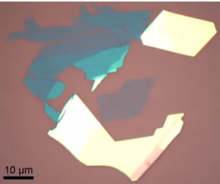
Figure 2-2. WS2 crystal example of the variety of crystal thicknesses achieved following mechanical exfoliation ranging from monolayer (light purple, center) to few-layer (blue, upper left) to multi-layer (yellow, bottom and upper right).
The main advantages of mechanical exfoliation as a method of producing monolayer TMD crystals are simplicity, versatility, and crystal quality. In terms of simplicity and versatility, a seminal paper in the field noted that “the whole procedure takes literally half an hour to
implement” and can be easily and equally applied to a wide range of layered crystalline materials such as BN, MoS2, NbSe2, Bi2Sr2CaCu2Ox and graphite.71 The quality of mechanically exfoliated
crystals, measured by point defect density, is a function of the method of production. Whereas CVD-grown crystals are nucleated and grown from the vapor phase on the time scale of minutes, and are therefore susceptible to high defect densities due to fluctuations in local concentrations and kinetic phenomena, mechanically exfoliated crystals are produced on much longer time scales (e.g., hours for synthetic bulk crystals and geological time scales for natural minerals) and therefore tend to equilibrate to thermodynamically preferred stoichiometries and defect densities.
The main disadvantages of this technique are the prevalence of organic residue, the lack of scalability, and the lack of capabilities to achieve complex structure formation. The organic residue (i.e., glue) on the SiO2 substrate and exfoliated TMD crystals comes from the adhesive as well as adsorbates from the environment.72 Appropriate choice of adhesive can limit the amount
32
of organic residue found on the substrate and crystals and cleaning steps can be taken to remove it.73 However, these cleaning steps much be chosen carefully to avoid damage to the TMD crystal. The scalability issues of mechanical exfoliation are largely irrelevant for academic research, but pose a fundamental limitation to the commercialization of any technology dependent upon this technique. Most mechanically exfoliated TMD crystals used in research have been produced manually by processes that involves several poorly controlled parameters (e.g., layer number of initial crystal and force of adhesive peeling). While steps can be taken to automate the exfoliation process, it will likely never achieve the level of reproducibility and control attainable by bottom-up methods such as CVD. Lastly, top-down methods such as mechanical exfoliation can break both chemical and vdW bonds, but cannot form chemical bonds. Therefore, while this technique is adequate for isolation of monolayers of pre-defined chemistries, it is incapable of producing complex chemically bonded structures through
advanced processing and patterning steps. When simplicity and quality are desired, mechanical exfoliation is effective and efficient. However, for advanced manufacturing, alternative
techniques such as CVD must be pursued. 2.1.2 Chemical vapor deposition
For wafer-scale fabrication of TMD-based electronic and optoelectronic devices, the use of a scalable technique such as CVD is necessary. The fundamental principle of CVD involves the vaporization of multiple precursor materials that will then adsorb on the target substrate and chemically react with each other to nucleate and grow crystalline material. This technique has been applied toward the synthesis of a large and growing list of TMDs and other 2D materials as well as the growth of heterostructures and alloys.74–83
33
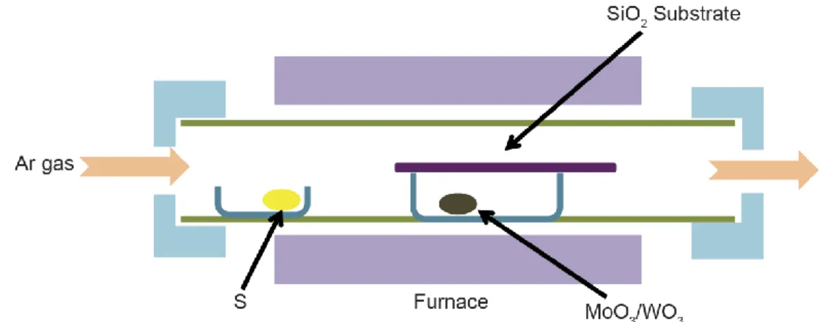
A typical set-up for a CVD system used for the growth of 2D TMDs involves the placement of precursor powders into alumina boats that are loaded into a quartz tube inside a tube furnace (Figure 2-3). A carrier gas will flow in from the upstream end of the tube to carry the vaporized precursor powders downstream toward the substrate. The effluent vapor will exhaust out of the downstream end of tube. This process contains a large number of tunable parameters which can make it difficult to optimize but can also enable a high degree of control. The key parameters can be grouped into the following categories which will be discussed in detail below: gas,
temperature, materials selection, and timing.
Figure 2-3. Schematic of a typical CVD furnace set-up identifying the relative locations of key components.
2.1.2.1 CVD gas parameters
The role of the input gas in a CVD system is to act as a carrier of the precursor vapor to the substrate and to define the environmental conditions in which the chemical and physical processes occur. There are typically three main CVD parameters related to the input gas: chemical choice, background pressure, and flow rate.
Ar and N2 are commonly chosen input gases due to their relative inertness, low cost, and ease of handling. H2 gas is a common additive (e.g., 10-15% mixture with Ar or N2) to create a
34
reducing environment favorable for growth of WX2.84–86 Conversely, H2O vapor has been demonstrated as useful additive to rapidly neutralize a H2-generated reducing environment and create an oxidizing environment to promote growth of MoX2. By alternating between reducing and oxidizing environments, multi-domain lateral heterostructures have been demonstrated with nearly atomically sharp interfaces.85 In the CVD experiments discussed throughout this thesis, Ar is used as the input gas.
The background pressure of the system controls the vapor transport mechanism between the precursor source and target substrate. The mean free path is calculated from the total pressure of the system by:
𝜆 (𝑐𝑚) ≈ 5𝑥10−3/𝑃 (𝑇𝑜𝑟𝑟) 2-1
Since our CVD system does not operate on the principle of “line of sight” deposition, the background pressure should be chosen such that the mass transport is viscous (i.e., diffusive) instead of molecular (i.e., ballistic) (Figure 2-4). Under viscous transport conditions, molecular collisions are expected and and the vapor flow outside the boundary layer of the substrate is assumed to be convective. Gas diffusivity is related to total pressure as well as gas temperature by:
𝐷𝑔𝑎𝑠∝ 𝑇32/𝑃 2-2
where gas temperature can be approximated by the temperature of the CVD zone. While some 2D TMD research has been conducted using low-pressure CVD to increase 𝐷𝑔𝑎𝑠 and thereby improve mass transport to the substrate,38,44,86–93 a significant amount of research including all of the results presented in this thesis has been conducted at atmospheric pressure.27,35,36,78,94–98
35
Figure 2-4. Gas flow regimes as a function of system dimensions and pressure. The approximate range of operating conditions reported throughout this thesis corresponds to the region within the grey rectangle in the viscous regime. Figure adapted from Ref. 99.
Whereas the background pressure controls the mass transport between the precursor source and target substrate, the flow rate dictates the behavior in the immediate vicinity of the substrate. With an immobile substrate and a non-zero flow rate, the boundary conditions of mass transport result in a stagnant film boundary layer (Figure 2-5):
𝑑𝑠𝑓 ≈ √𝜇𝑥/𝜌𝑈 2-3
where 𝜇 is the viscosity of the gas, 𝑥 is the distance from the leading edge, 𝜌 is the density of the gas, and 𝑈 is the bulk velocity of the gas. From the boundary layer thickness and gas diffusivity, the gas phase mass transport coefficient can be calculated as:
ℎ𝐺 = 𝐷𝐺/𝑑𝑆𝐹 2-4
In the bulk gas, the concentration of precursor vapor can be approximated as uniform and is determined by the precursor vaporization rate. Within the boundary layer, the concentration will
36
decrease as there is a net flux of precursor out of the bulk gas and onto the substrate where it is deposited. This can be modeled by a mass transport flux:
𝐹1 = ℎ𝐺(𝐶𝐺− 𝐶𝑆) 2-5
where 𝐶𝐺 is the bulk gas concentration and 𝐶𝑆 is the gas concentration at the substrate interface, and a reaction flux:
𝐹2 = 𝑘𝑆𝐶𝑆 2-6
where 𝑘𝑆 is a surface reaction rate constant which is dictated by adsorption and desorption rates that will be expanded upon in Section 2.1.2.2. Combining these equations together, the mass transport-limited growth regime is related to the macroscopic gas flow rate processing parameter by 𝐹1 ∝ 𝑈12, indicating that higher flow rates result in higher mass transport flux.
Figure 2-5. Schematics of (a) the stagnant film boundary layer, (b) concentration profile, and fluxes.
2.1.2.2 CVD temperature parameters
The three thermally-sensitive components of the CVD growth of 2D TMDs are the chalcogen precursor, metal precursor, and substrate. In a one-zone furnace (see Figure 2-3), it can be
difficult to de-couple the temperatures of these three components, often resulting in identical substrate and metal precursor temperatures and slightly lower chalcogen precursors depending
37
on the exact placement of the that respective alumina boat relative to the center of the furnace. Conversely, in a three-zone furnace (Figure 2-6), each component can be placed in its own heating zone, thereby allowing independent control of the temperature parameter for all three components. For additional temperature control, a push rod and pair of magnets can be used to change the position of the chalcogen precursor boat throughout the CVD growth process.
Figure 2-6. Schematic of a three-zone CVD furnace set-up demonstrating the ability to achieve thermal de-coupling of each precursor as well as the substrate.
The chalcogen precursor and metal precursor temperatures are relatively straightforward parameters. In each case, a growth temperature should be chosen to allow for vaporization of the precursor powder at a steady rate described by:
𝑅𝑒 ∝ 𝑇−
1
2𝑒𝑥𝑝(−ℎ𝑣𝑎𝑝/𝑘𝐵𝑇) 2-7
This temperature is typically in the range of 120-200 °C for S and Se precursor
powders,31,100–102 650-800 °C for MoO3 precursor powder,27,49,63,75,78 and 900-1100 °C for WO3 precursor powder.80,86,95,102
Due to the relatively high temperature necessary for WO3 vaporization and the consequent discrepancy in the vaporization rates of MoO3 and WO3 for any fixed temperature, there has been an effort to identify ways to lower the W precursor growth temperature to facilitate the controlled synthesis of mixed-metal alloys and heterostructures. One method that is becoming increasingly popular is mixing of alkali metal halide additives (e.g., NaCl) to the transition metal
38
precursor powder to volatilize the precursor and reduce its vaporization temperature.96,103–105 While this method is effective, it also places additional emphasis on the importance of controlling relative precursor vaporization rates. That is, if the metal precursor CVD zone temperature is not adequately adjusted to the vaporization temperature, accounting for any possible additives, then the metal precursor will vaporize at a rate that is incompatible with the vaporization rate of the chalcogen precursor.
The relative vaporization rates of the chalcogen and metal precursors affect the vapor concentrations of those precursors and the eventual stoichiometry of the grown crystal. As the M:X ratio of the MX2 TMD deviates from 1:2, the crystal will become rich in one precursor and deficient in the other. The hexagonal crystal structure implies that a crystal with a balanced stoichiometry will be macroscopically hexagonal with three chalcogen-terminated edges and three metal-terminated edges. To accommodate imbalances in stoichiometry, the crystal will become macroscopically triangular, comprised exclusively of the three ZZ edges terminated by the element in surplus. In the extreme case, this imbalance can eventually lead to high
probabilities of defect formation as well as undesirable dendritic morphologies.94,106
When the substrate temperature can be de-coupled from the metal vaporization temperature, as is the case in multi-zone furnaces, greater consideration must be given to this parameter as it affects the kinetics of the precursor flux as well as the nucleation and growth of the TMD crystal. As described earlier in Section 2.1.2.1, the two fluxes that describe precursor deposition on the substrate are the mass transport flux and the chemical reaction flux. The mass transport flux is sensitive to gas flow rate, but also contains a temperature component through the gas diffusivity equation. The temperature relation of crystal growth in the mass transport-limited regime is therefore modeled as 𝐹1 ∝ 𝑇𝑠𝑢𝑏𝑠𝑡𝑟𝑎𝑡𝑒
3/2
39
low flow rates and is relatively insensitive to temperature and relatively sensitive to flow rate (Figure 2-7).
In addition to mass transport flux, the concentration gradient in the boundary layer is also described by the surface reaction flux (Equation 2-6). As a thermally activated process, a first-order equilibrium reaction rate can be modeled by as:
𝑘𝑠 = 𝑘0exp(−𝐸𝑎/𝑘𝐵𝑇𝑠𝑢𝑏𝑠𝑡𝑟𝑎𝑡𝑒) 2-8
Consequently, when the gas flow rate is high and/or the substrate temperature is low and the system is operating in a reaction-limited regime, the reaction flux and therefore also the growth rate are related to the substrate temperature by 𝐹2 ∝ exp(−1/𝑇𝑠𝑢𝑏𝑠𝑡𝑟𝑎𝑡𝑒).
Figure 2-7. Schematic plot of the temperature dependence of the growth velocity in different growth regimes.
The surface reaction flux refers to the difference between adsorption and desorption of the precursor vapor. This non-zero difference results in the accumulation of adsorbed material that can undergo a variety of temperature-dependent phenomena including surface diffusion, adatom clustering (i.e., crystal nucleation), and crystal growth. Adatoms will diffuse across the surface of
40
a substrate by a series of atomic jumps from potential energy well to potential energy well. Those jumps will collectively form a random walk in the absence of an energy gradient and a correlated walk in the presence of an energy gradient. The temperature-dependent jumping rate is modeled as:
Γ = 𝜈 exp(−𝐸/𝑘𝐵𝑇𝑠𝑢𝑏𝑠𝑡𝑟𝑎𝑡𝑒) 2-9
where 𝜈 is the attempt frequency derived from a simple harmonic oscillator model and 𝐸 refers to the energy barrier between neighboring potential wells. The 2D surface diffusion coefficient can be calculated from jumping rate as:
𝐷 = Γ𝑎2/4 2-10
where 𝑎 is the distance per jump.
As the number of atomic jumps and the number of adatoms increase, the probability of adatom-adatom interaction also increases. As adatoms interact with each other, they will tend to form thermodynamically stable clusters (i.e., nuclei) of atoms. The temperature-dependent steady-state distribution of the 𝑛 number of clusters containing 𝑁 atoms can be modeled as:
𝑛𝑁/𝑛1 ≈ exp(−Δ𝐺𝑁/𝑘𝐵𝑇) 2-11
Approximating a TMD nucleus as a 2D disc, the free energy can be modeled as:
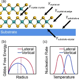
Δ𝐺𝑟,𝛾 = 𝜋𝑟2𝑧Δ𝐺𝑣𝑜𝑙 + 𝜋𝑟2(𝛾𝑐 + 𝛾𝑠𝑐− 𝛾𝑠) + 2𝜋𝑟𝑧𝛾𝑐,𝑒𝑑𝑔𝑒 2-12
where 𝐺 is free energy, 𝑟 is radius, 𝑧 is thickness, 𝛾 is surface energy, and the surface energy subscripts refer to the crystal-air, substrate-crystal, and substrate-air planar interfaces and the crystal-air edge interface, respectively.32 Beyond the critical cluster radius where 𝜕Δ𝐺/𝜕𝑟 = 0, it
41
becomes energetically favorable for nuclei to continue to grow into larger crystals. Optimal CVD growth should operate in a substrate temperature range that allows for a sufficient amount of surface diffusion of adatoms to occur between adsorption and desorption events to allow nuclei to form and grow to the critical size necessary for stability and continued growth. Adjustments within this process parameter range will affect nucleation density, which then affects grain size.
On a properly cleaned substrate, deposited TMD material can either nucleate a new
monolayer crystal on the substrate, attach to the edge of an existing TMD crystal to contribute to crystal growth, or nucleate a new layer on top of an existing TMD crystal. Similarly, in
heterostructure formation, new chemical domains can also nucleate by attaching to the edge of an existing TMD crystal to form a lateral heterostructure or on top of existing TMD crystals, which would form vertical heterostructures. The kinetics of these possible processes are dictated by substrate temperature and the relative surface energy values of the relevant TMD and
substrate interfaces through the surface diffusion, nucleation, and free energy model equations discussed earlier (Equations 2-10 through 2-12, respectively) and demonstrated in Figure 2-8. In the case of monolayer vs. multilayer growth of a single TMD chemical domain32 as well as lateral vs. vertical TMD heterostructure growth,24 lower substrate temperatures tend to favor lateral monolayer crystal growth with a TMD-substrate planar interface whereas higher substrate temperatures tend to favor vertical multilayer growth with a TMD-TMD planar interface.
42
Figure 2-8. Energetics for calculating critical nucleation size and monolayer vs. multilayer growth. Figure adapted from Ref. 32.
2.1.2.3 CVD materials selection
The materials selection requirements for CVD growth of TMD materials involve the choice of a chalcogen precursor, transition metal precursor, substrate, and any possible additives (e.g., NaCl discussed in Section 2.1.2.2) to aid the growth process. In the CVD experiments discussed throughout this thesis and in the majority of the literature in the field, the chalcogen precursor powder is the elemental solid powder of the chalcogen material (i.e., S, Se, or Te) whereas the transition metal precursor is in the form of a metal trioxide (e.g., MoO3 or WO3). Other demonstrated transition metal precursors include ammonium-based precursors (e.g.,
(NH4)2MoS4),77,107 elemental metal films,108 and metal chlorides (e.g., MoCl4).109 Precursor selection can also vary by the selection of a non-CVD deposition technique such as metal-organic CVD and molecular beam epitaxy. Metal-metal-organic CVD has been demonstrated using metal hexacarbonyls (e.g., Mo(CO)6), diethyl sulfide (i.e., (C2H5)2S), and dimethylselenium (i.e., (CH3)2Se).40,110–112 Molecular beam epitaxy of 2D TMDs has also been demonstrated using high-purity elemental sources.113–118