Architectures and System Design for Digitally-Enhanced
Antenna Arrays
by
James David Stone Krieger
B.S., University of California at Santa Barbara (2000)
M.S., The Ohio State University (2005)
Submitted to the Department of Electrical Engineering and Computer Science
in partial fulfillment of the requirements for the degree ofDoctor of Philosophy in Electrical Engineering and Computer Science
MASSACHUSESM IRS E
at the OF TECHNOLOGY
MASSACHUSETTS INSTITUTE OF TECHNOLOGY
APR
0
2014
February 2014 ~ ~R ~
LIBRARIES
@Massachusetts
Institute of Technology 2014. All rights reserved.Author ...--A u th r . .... - ... . .. . .. .... .. ... ... 3...
t ent-of-EBectrical Engineering and Computer Science
October 28, 2013
I
V .. . . . . .-.Professo of lectrical
Accepted by ...
Gregory W. Wornell Engineering and Computer Science Thesis SupervisorChair, Committee
Leslie A. Kolodziejski
on Graduate Students
Certified by....
,a
ANOW
Architectures and System Design for Digitally-Enhanced Antenna Arrays
byJames David Stone Krieger
Submitted to the Department of Electrical Engineering and Computer Science on October 28, 2013, in partial fulfillment of the
requirements for the degree of
Doctor of Philosophy in Electrical Engineering and Computer Science
Abstract
Digital techniques have had longstanding use in both the operational control and signal processing efforts associated with phased array antennas. Fundamentally, these techniques have served to provide additional levels of convenience and performance over the fully analog counterparts, without specifically addressing the underlying design of the analog hardware aspects of the arrays. The class of digitally-enhanced hardware has recently emerged, wherein "digitally aware" design approaches are used for the purpose of alleviating the high cost and complexity of sophisticated analog devices.
Emergent trends in millimeter wave and low-terahertz circuit technology are enabling the prospect of physically small, yet electrically large antenna arrays for a host of exciting new communication, radar, and imaging applications. Still, the high cost of phased arrays remains a significant bottleneck to any widespread deployment in this regard. In light of this challenge, we propose two phased array architectures for which the notion of digital awareness plays a central role in their designs.
The Dense Delta-Sigma Array: Primarily motivated by advancements in low-cost fabri-cation, this design concept provides the opportunity to replace the expensive RF components required to control the individual array element excitations with inexpensive phase shifter components having particularly coarse resolution (as few as 2-bits). This is made possible
by increasing the number of array elements for a given aperture beyond the nominal number
associated with the standard half-wavelength spacing. This approach is inspired by Delta-Sigma data converters, which employ faster-than-Nyquist sampling with low quantization resolution.
The Sparse Multi-Coset Array: This design concept exploits the sparsity commonly found in typical environments to allow for target detection and imaging with significantly fewer array elements than prescribed by conventional half-wavelength spacing. The result is a structured periodic non-uniform array composed of a number of distinct subarrays known as cosets. This approach is inspired by multi-coset sampling, for which the average sampling rate may be reduced below the Nyquist convention when the spectral components within the overall bandwidth are limited to some number of sub-bands. In this approach, we view the underlying engineering design problem as one of compressive sensing.
In this thesis, we develop and apply the underlying mathematical principles and concepts of the dense and sparse arrays, taking into account the practical constraints and issues that make the system design, analysis, and performance evaluation rich from an engineering perspective.
Thesis Supervisor: Gregory W. Wornell
Acknowledgments
My time at MIT has been a life changing experience, and I owe many thanks to many
people. Nearly every interaction I have had during my time here-from the courses I have taken to the group meetings and seminars to the numerous individual conversations-has left me feeling a little more complete.
I am particularly grateful to have had Greg Wornell as my adviser. I consistently found myself challenged in our research, and as I finish my time here I feel as though his guidance and direction have laid a foundation for a new way of thinking that I have only begun to explore. Plus, as large of a challenge as it must have been on his end, he always managed to keep me pushing forward when I felt like I didn't have it in me. Truly, thank you so much for everything.
I also want to thank my wonderful thesis committee: Charlie Sodini, Yuval Kochman, and Alan Fenn. Each of you brought unique insights and perspectives and I am all the better for it. I hope our paths continue to remain close for a long time.
MIT Lincoln Laboratory played a huge role in getting me to this point. I thank the Lincoln Scholars Committee for making all of this possible, Jeff Herd and Helen Kim for all of their support and guidance, and Leonard Parad. Extra special thanks to Dave Bruno and Glenn Brigham for making the experimental portions of this thesis possible.
It was a great experience getting to work with all of the present and past members of the Signals, Information, and Algorithms group, especially my on-again, off-again office-mate Da Wang, who put up with my endless questions about all manners of things. I particularly want to thank Tricia O'Donell and Janet Fischer for all their help with so much.
And of course, my love and thanks to my wonderful family: my fancy siblings Leah, Brian, and Ross; my dearest mother, Mum; and my Papa for being such a huge support during these past few months, always reminding me to breathe and telling me to "go do my homework". I love you all!
This work was supported in part by DARPA under Contract No. HR0011-06-1-0004,
by the Semiconductor Research Corporation through the FCRP Center for Circuit and
Sys-tem Solutions (C2S2), and by the Department of the Air Force under Air Force Contract
No. FA8721-05-C-0002. Opinions, interpretations, conclusions and recommendations are
Contents
1 Introduction 15
1.1 M otivation . . . . 15
1.2 Research Philosophy . . . . 16
1.3 Related Work . . . . 18
1.4 Contributions and Thesis Structure . . . . 21
2 Conventional Phased Array Concepts 23 2.1 Linear Arrays of Isotropic Elements . . . . 23
2.1.1 Array patterns . . . . 23
2.1.2 Beam scanning . . . . 23
2.2 Mutual Coupling . . . . 26
2.3 Power Efficiency . . . . 28
3 Delta-Sigma Quantization for Phased Arrays 31 3.1 Traditional Delta-Sigma Quantization Concepts . . . . 31
3.1.1 Oversampling . . . . 31
3.1.2 Noise shaping . . . . 32
3.2 AE Phased Arrays . . . . 34
3.2.1 Conventional phase quantization . . . . 35
3.2.2 AE phase quantization . . . . 37
3.3 Delta-Sigma Implementation . . . . 39
3.4 Phase Errors . . . . 41
3.5 Array Theory Perspective . . . . 42
3.6 Delta-Sigma Planar Arrays . . . . 44
4 Mutual Coupling Effects 53 4.1 Mutual Coupling in Dense Arrays . . . . 53
4.2 Narrowband Efficiency . . . . 54
4.3 Wideband Performance . . . . 65
4.A Matched Array Coupling Matrix Derivation . . . . 68
5 Delta-Sigma Measurements 69 5.1 Measurement Description . . . . 69
5.2 Analysis and Results . . . . 72
5.3 R em arks . . . . 80
6 Sparse Multi-Coset Arrays 85
6.1 Array Structure and Scene Model ... ... 86
6.2 Multi-Coset Imaging Principles . . . . 88
6.2.1 Reconstruction with known support . . . . 89
6.2.2 Support recovery . . . . 91
6.2.3 Coset period selection considerations . . . . 93
6.3 Multi-Coset Array Processing . . . . 93
6.3.1 Reconstruction noise amplification . . . . 93
6.3.2 Support recovery reliability . . . . 95
6.4 Support Recovery Failure Detection . . . . 98
6.4.1 Failure detection in the absence of noise . . . . 98
6.4.2 Failure detection in the presence of noise . . . . 99
7 Multi-Coset Array Design and Application 101 7.1 High SNR Designs . . . . 101
7.2 Low SNR Designs . . . . 102
7.3 Pattern Computation, Evaluation, and Comparison . . . . 103
7.4 Range-Azimuth 2-D Imaging Simulations . . . . 106
7.4.1 Range-dependent scene sparsity . . . . 106
7.4.2 2-D imaging illustration . . . . 106
7.4.3 Undersparse arrays . . . . 112
8 Multi-Coset Array Experimental Validation 115 8.1 Hardware description . . . . 115
8.2 Test Configuration and Layout . . . . 116
8.3 Measurement Description . . . . 119
8.4 Multi-Coset Image Results . . . . 123
8.5 R em arks . . . . 124
9 Conclusions and Future Work 127 9.1 Delta-Sigma Amplitude Tapering . . . . 131
9.2 Topics in Random Matrix Theory in Multi-Coset Analysis . . . . 133
9.3 Nested Multi-Resolution Multi-Coset Arrays . . . . 134
9.4 "Ultra-Sparse" Multi-Coset Arrays . . . . 135
9.4.1 Planar multi-coset arrays . . . . 137
9.4.2 Multi-coset MIMO radar . . . . 138
List of Figures
1-1 Illustration of range-dependent sparsity. . . . . 17
2-1 Uniform linear array geometry . . . . 24
2-2 Power patterns for L = 20A linear array scanned to kzo = k/2. The edges of the visible region are marked with vertical dotted lines. . . . . 25
2-3 Equivalent circuit diagram for the antenna array. The beamformer output is described by a set of voltage sources {wn}, each with internal impedance ZO. The mutual coupling among the array elements is modeled as a N-port network with impedance matrix Z. . . . . 27
3-1 Sampled-data equivalent circuit of a conventional analog-to-digital converter. 32 3-2 Equivalent circuit of the AE analog-to-digital converter. . . . . 33
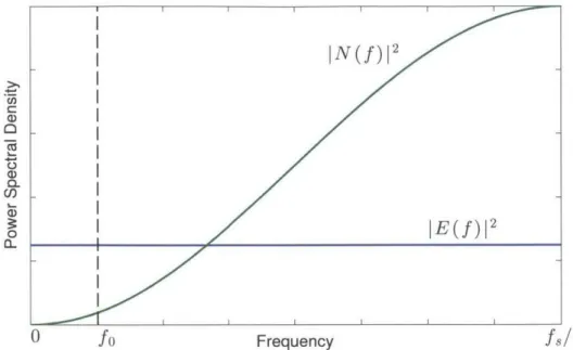
3-3 Power spectral density of the noise IN(f)|2 from AE quantization compared with that of conventional quantization JE(f)12, OSR = 8. . . . . 34
3-4 Equivalent circuit for conventional phase quantization. . . . . 35
3-5 Equivalent circuit for AE phase quantization. . . . . 38
3-6 AE SQNR results for uniform amplitude scanning array of length L = 20A. 41 3-7 Comparison of effects of random phase errors with standard deviation o radians on SQNR for (a) conventional quantization and (b) AE quantization. 43 3-8 Power pattern for a two-element array with excitation weights wo 1 and
w,
= -1. The edges of the visible region are marked with vertical dotted lines. ... 443-9 Power patterns P(kz) (ideal weights) and P (kz) (AE weights) for arrays of length L = 20A scanned to kzo = 0.045k for density factors (a) R = 1 (b) R = 2 and (c) R = 4. . . . . 45
3-10 1-D error passing . . . . . 46
3-11 1-D error kernel . . . . ... . . . . 46
3-12 2-D error passing... ... 47
3-13 2-D error kernel associated with Figure 3-12. . . . . 48
3-14 2-D AE kernel pattern for R = 4. . . . . 49
3-15 Alternative symmetric 2-D error kernel. . . . . 49
3-16 Alternative 2-D AE kernel pattern for R = 4. . . . . 50
3-17 Relative noise power for both 2-D AE kernels. . . . . 51
4-1 (a) Magnitude of the coupling coefficients {cp} for a central element in an array of length L = 20A, with R = 4. (b) Power pattern response Pc(kz) = Ifc(k,) 2 for an array excited by the coupling coefficients. . . . . 55
4-2 Quantization error (power) patterns for the AE array of length L = 20A using both the forced and free excitation models with density ratios (a) R = 1 (b)
R = 2 and (c) R = 4. . . . . 56
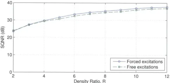
4-3 Comparison of SQNR versus density ratio R for AE arrays based on the forced and free excitation models. L = 20A. . . . . 57
4-4 (a) Real part and (b) imaginary part of the average scan impedance of ele-ments in an array of length L = 20A, for density ratios R = 1 and R = 2. Calculations include scan impedance matching network designed for perfect match to Zo = 1 at ko = 0. . . . . 59
4-5 Power efficiency as a function of scan angle kzo, L = 20A, R = 4, with scan impedance matching network designed for perfect match at ko = 0. Results for the AE array obtained by setting & = 1.26a such that the nominal efficiency is within approximately 2 dB of the ideal result. . . . . 61
4-6 SQNR dependence on density ratio R for AE arrays using forced excitations and free excitations with matching network designed for ideal match at ko = 0. Array length L = 20A. . . . . 62
4-7 Nominal power efficiency loss versus the ratio of the AE and ideal array weight magnitudes 7 = &/a. The dashed grey line shows the corresponding estimated value of p given by (4.7). . . . . 63
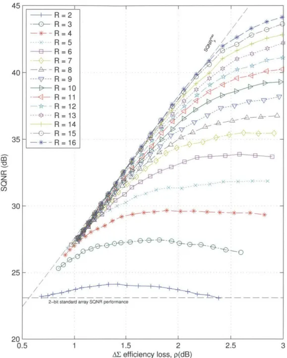
4-8 SQNR versus power efficiency loss for the length L = 20A array. . . . . 64
4-9 Wideband efficiency performance results from numerical simulations for array length L = 20A. . . . . 67
5-1 12 x 12 array used for measurements. . . . . 70
5-2 Mounted test array in anechoic antenna measurement chamber. . . . . 70
5-3 Single element gain measurement connection. . . . . 71
5-4 Measured element (a) gain (b) phase patterns at 4 GHz. . . . . 73
5-5 Measured element (a) gain (b) phase patterns at 5 GHz. . . . . 74
5-6 Measured element (a) gain (b) phase patterns at 6 GHz. . . . . 75
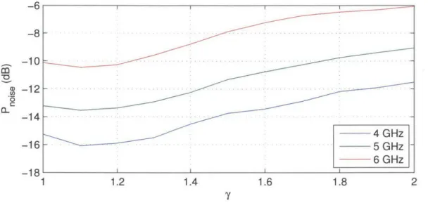
5-7 Average quantization noise power dependence on the AE amplitude ratio y for the measured array . . . . 76
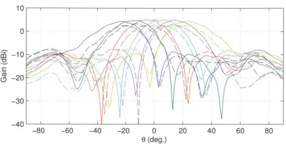
5-8 12 x 1 array beamformed gain patterns for the ideal (solid) and AE (dashed) array weights at scan angles 0= {-25', -15', -5', 5', 15', 25'} at 4 GHz. . 77 5-9 12 x 1 array beamformed gain patterns for the ideal (solid) and AE (dashed) array weights at scan angles O0 = {-25', -15', -5, 50, 15', 25'} at 5 GHz. . 78 5-10 12 x 1 array beamformed gain patterns for the ideal (solid) and AE (dashed) array weights at scan angles 0= {-25', -15', -5', 50, 15', 2501 at 6 GHz. . 78 5-11 Frequency dependence of AE quantization noise power from measured results. 79 5-12 Frequency dependence of ideal and AE power efficiencies from measured results. 80 6-1 Imaging array geometry. . . . . 86
6-2 (P, L) = (4, 7) multi-coset array with coset pattern 'P {0, 1, 2, 4} and M = 6 coset periods. . . . . 87
6-3 (Q, L) = (3, 7)-sparse scene with support Q = {1, 2, 4} . . . . 88
6-4 Multi-coset reconstruction processing chain. . . . . 90
6-5 Empirical recovery probability versus SNR for L = 19, P = 9, and (a) Q = 6 (b)
Q
= 7 (c)Q
= 8. . . . . 97LIST OF FIGURES
6-7 Normalized BPE versus
Q,
at different SNR, L = 19, P = 9. The solid and dashed portion of each curve represent the successful and failed cases,respectively. . . . . 100
6-8 Normalized BPE threshold versus SNR, L = 19, P = 9. . . . . 100
7-1 Recovery probability vs SNR for (a) (L, P,
Q)
= (7, 3, 2) and (b) (L, P,Q)
= (13, 4 , 3) . . . 1057-2 Point source model. . . . . 107
7-3 Standard array image reconstruction, N = 987 elements with spacing do = Ao/2. SNR = 30 dB. . . . . 108
7-4 Reconstructed image for the (28, 47) multi-coset array. SNR 30 dB. . . . 109
7-5 Reconstructed image from the sparse uniform array of N 588 elements with spacing d = do/0.596 = 0.839A. SNR = 30 dB. . . . . 110
7-6 Reconstructed image for the (28, 47) multi-coset array with "bunched" coset pattern Pb = {0, 1, ... , 27}. SNR = 30 dB. . . . . 110
7-7 Standard array image reconstruction, N = 987 elements with spacing do = Ao/2. SNR = 10 dB. . . . .111
7-8 Reconstructed image for the (28, 47) multi-coset array with coset pattern P as in Figure 7-4. SNR = 10 dB. . . . .111
7-9 Reconstructed image for the (28, 47) multi-coset array with "bunched" coset pattern Pb = {0, 1,..., 27}. SNR = 10 dB. . . . . 112
7-10 Multi-coset images with failure detection, L = 47 and (a) P = 14, (b) P = 9, (c) P = 5. SNR = 30 dB. . . . . 113
8-1 Radar antennas used in multi-coset measurements. . . . . 116
8-2 Mounting rail with markings indicating measurement locations. . . . . 117
8-3 Rail-mounted radar in experimental setting. . . . . 118
8-4 Corner reflectors used as target objects for measurements. . . . . 118
8-5 Target setup. ... .... .... ... .... 119
8-6 Experimental layout and geometry. . . . . 120
8-7 Full array image in p-range space. . . . . 121
8-8 Full array image in cartesian coordinates. . . . . 122
8-9 Reconstructed image result and range dependent back projection error from measured data for an array sparsity of 71.4%. L = 7, P = 5, P = {0, 1, 2, 3, 5}.123 8-10 Reconstructed image result and range dependent back projection error from measured data for an array sparsity of 57.1%. L = 7, P = 4, P = {0, 1, 2, 4}. 124 8-11 Reconstructed image result and range dependent back projection error from measured data for an array sparsity of 42.9%. L = 7, P = 3, P = {0, 1, 3}. . 125 8-12 Reconstructed image result and range dependent back projection error from measured data for an array sparsity of 28.6%. L = 7, P = 2, P = {0, 1}. . . 125
9-1 Power patterns for ideal and AE arrays of length L = 20A with 30 dB Taylor w indow s. . . . . 132
9-3 Characterization of array resolution versus maximum scene sector occupancy
(Qmax = P-1) for the 24 element MRMC array shown in Figure 9-2 [cf. (9.1)].
Circular markers along the dashed line represent four distinct fixed multi-coset array geometries. Square markers along the solid line denote the three
operational states simultaneously available to the MRMC array. . . . . 136
9-4 Planar multi-coset array on rectangular lattice. . . . . 137
9-5 Planar multi-coset array on hexagonal lattice. . . . . 138
9-6 SIMO radar and equivalent MISO radar systems. . . . . 139
9-7 MIMO radar and equivalent virtual SIMO radar systems. . . . . 139
List of Tables
4.1 Comparison of several array configurations for AE arrays of length L = 20A. 65 7.1 Examples of coset patterns P* selected according to the co-array approach. 103 7.2 Maximum condition numbers,
Q
= P - 1. . . . . 1047.3 Examples of coset patterns P* found using MCMC. . . . . 105 9.1 Total number of elements N + N, in the (SIMO) multi-coset and MIMO
multi-coset systems for M = 21 coset periods of L = 47. Sparsity percentages shown in reference to total number of elements in the conventional SIMO system , 1 + M L = 988. . . . . 140
Chapter 1
Introduction
Digital techniques play a prominent role in nearly all modern phased array systems, enrich-ing both their operational and signal processenrich-ing capabilities in ways beyond the possibility of the original analog designs. The implementation of digital control over the amplitudes and phases of the array element weights permits the rapid electronic reconfiguration of the array pattern characteristics. The many developments in digital array processing have yielded numerous additional tools for the extraction of useful information that would be impossible or far less practical to implement through fully analog designs.
While these digital approaches complement the phased array system in a number of ways, these systems still rely on conventional front-end designs having a high level of precision in the complex signal weights at each of the individual elements. Put another way, while the algorithmic design must account for the specifics of the analog design, the array is designed without regard for the digital aspects of the system.
Recently, there has been an emergence of digitally-enhanced hardware designs motivated
by the desire to bridge the gap to cooperative design approaches that emphasize a level of
awareness regarding the utilization of digital techniques such that the requirements for ana-log device complexity can be relaxed. The existing integration of digital system blocks so common in phased arrays makes them natural candidates for such enhanced techniques. Further, as advances in circuit technologies at increasingly higher frequencies surface, new frontiers for the use of phased arrays become reality. Yet with the existing design conven-tions, the phased array is normally considered to be a prohibitively costly and complex antenna option, emphasizing the pressing need for a shift in perspective in order to address the challenges of making their widespread use a possibility. As such, this thesis presents two alternative phased array architectures that use digital perspectives in both design and operation. In both cases, the architecture moves beyond conventional design principles in a way that provides new opportunities for cost reductions while avoiding the limitations common to existing array design techniques.
1.1
Motivation
Since the development of phased array antennas, they have been the ideal choice for a vast range of applications ranging from point-to-point communication to remote sensing and more recently, to high resolution imaging systems, to name just a few. Unfortunately, the same design features that allow the performance and flexibility characteristics that make phased arrays desirable come at such high costs as to preclude their use in all but
a relatively small number of highly sophisticated systems. Research efforts promoting the evolution of phased array designs aimed at overcoming this issue have been limited for several decades, resulting in a general acceptance of the impracticality of a more pervasive presence. However, as we look to the future, it becomes increasingly clear that the need to meet these design challenges must be acknowledged.
Recent advances in technology at the millimeter-wave and the low terahertz frequency ranges-in both the development of circuitry as well as lithography at these scales-has enabled the potential for a new generation of portable high-end and consumer electronics. Although size and fabrication issues are more manageable than ever before, the costs associ-ated with the circuitry required for element level control remains a significant bottleneck to making this a reality. Though the goal of designing low-cost phased arrays is longstanding, these new possibilities motivate the need for novel perspectives.
1.2
Research Philosophy
Historically, the attempts in making the phased arrays more affordable have involved ad-justing hardware designs. More recently, there has been growing interest in the design of "digitally enhanced" analog circuits to leverage digital techniques and the increasing avail-ability of low-cost processing power to alleviate the need for high precision, high complexity analog blocks; see, e.g., [1] and references therein. This philosophy inspires the two novel array architectures that are the focus of this thesis.
Dense Delta-Sigma Phased Array
The most common of phased array designs use digital phase shifters at each element. A phase shifter having M-bits of resolution can be used to adjust the phase at an individual element by one of 2M levels, with the exact shift implemented digitally by a dedicated
processor. For a given beam pattern, this processor determines the ideal phase shift to be applied for each element, and then selects the nearest quantized phase shift from the available 2M levels. Consequently, the level of quantization distortion in the overall array
pattern increases as the precision of the phase shifters decrease. As such, most phased arrays use a minimum of 4- or 5-bits of resolution in order to keep this distortion at acceptably low levels.
The Delta-Sigma (AE) phased array differs from conventional designs in three primary ways. Unlike conventional array designs, in which the elements are uniformly spaced by a distance do = A/2, where A is the operating wavelength of the array, the AE array is
dense: a greater number of elements are packed into a given aperture such that the uniform
spacing is d < do. Instead of the high-precision components used to set the amplitude and phase adjustments to the signals at the array elements, or array weights, the AE array uses only 2-bit phase shifters, limiting the weights to only four possible values. The selection of the appropriate quantized phase shift no longer selects the "closest value" to the ideal phase shift.
It is well known from conventional array theory that this dense element spacing does not add to the array performance in the case of ideal weights. However, in practical set-tings where the array weights are quantized, this close element spacing affords additional flexibility in controlling the amount of distortion caused by this quantization. By making use of the digitally controlled analog architecture, the availability of inexpensive processing power is used to account for the effects of quantization by selecting the weights in a manner
1.2. RESEARCH PHILOSOPHY
Figure 1-1: Illustration of range-dependent sparsity.
that uses neighboring elements to cancel out distortion. As the distance between the ele-ments decreases, the effectiveness of this cancellation technique improves. As we will see, the distortion caused by the use of the 2-bit phase shifters can be made arbitrarily small. Sparse Multi-Coset Imaging Array
In a traditional linear imaging array, when the elements are arranged with uniform element
spacing do = A/2, where A is the wavelength of the received signal, the image resolution improves in direct proportion to the number of elements No. In the multi-coset imaging array, the same aperture length Nodo uses N < No elements to produce an image at the same resolution as the conventional imaging array. When fewer than No elements are uniformly spaced by d > do, this leads to spatial aliasing, or grating lobes, producing images with copies of the targets appearing at additional incorrect locations. In the multi-coset array, the elements are positioned in a recurrent nonuniform arrangement in such a manner that the presence of such grating lobes can be avoided.
The ability to obtain the correct image using a reduced number of elements is based on the observation that target scenes are themselves sparse in most cases. That is, the image will contain a certain number of locations that are empty of any targets. While this is not necessarily the case when considering the fraction of directions in which targets are located, the existence of scene sparsity is apparent when one considers the ability to distinguish the distance to targets by sorting their responses into a number of range cells. In light of this, scene sparsity can be regarded as the portion of directions occupied by targets within each range cell. As a simple example, Figure 1-1 illustrates this effect. In the illustration, the array, shown in green, faces a large object, shown in grey, with the faces shown in red representing the surface of this object in the field of view of the array. The complete surface surrounds the array such that the scene taken as a whole exhibits no sparsity whatsoever. However, if the scene is sorted into separate range cells, as shown by the concentric blue half-circles, it is only the intersection of the red surface with the individual cells that defines the relevant level of sparsity.
The multi-coset architecture permits a reduction in the required number of elements to an array density ratio N/No provided this relative density remains above the scene density
over all range cells. Rather than using conventional imaging-a digital implementation of analog beamforming-the digital processing is enhanced through the use of an imaging algorithm that first examines the received signal data to determine the angular regions in which targets are located, and then utilizes the knowledge of this reduced angular subspace to solve for the image response within this region.
1.3
Related Work
This research builds on a number of contributions from a range of communities. In this section, we summarize some of the related works from the fields of antenna theory, signal processing, circuit design, and compressive sensing to provide context for the contributions of this thesis.
Cost Effective Array Designs and Delta-Sigma Applications
The developments in millimeter-wave technology have led to a resurgence of interest in practical phased array designs tailored to this new frequency regime; see, e.g., [2-7] and the
references therein. Within the broader realm of ongoing research, some efforts are focused primarily on exploiting increasing levels of silicon integration, while other efforts primarily seek to exploit the increasing availability of inexpensive digital circuitry and processing. Moreover, some of the most promising efforts leverage both jointly.
In spite of recent progress, the components required for accurate phase control at each element in such arrays continue to be expensive, precluding the use of phased arrays in many otherwise compelling applications. Simply replacing high-end, high-resolution components with low-cost, coarsely discretized phase shifters in traditional designs sharply degrades performance, limiting the quality of the beams that can be formed by the array. As a result, addressing the need for adequate phase control in beamforming remains a key challenge in the pursuit of widespread deployment of millimeter-wave phased arrays.
There has been a variety of research exploring this issue. For example, some research has focused on characterizing the capabilities of phased array systems utilizing low resolution phase shifters to meet the needs of current and proposed millimeter-wave applications [8,9]. At the same time, other research has focused on developing novel approaches for sharing a smaller number of phase shifters (and other components) among antenna elements
[10].
In this design, we explore a rather different approach. Specifically, instead of pursuing designs with a smaller number of accurate phase shifters, we develop a high-performance architecture based on efficient utilization of a larger number of coarse phase shifters. To accomplish this, we repurpose the established theory of delta-sigma analog-to-digital con-verters (ADCs) [11], applying it in the spatial domain to determine an appropriate phase for each of the densely packed elements to create a desired array pattern. In temporal domain
AE as used in ADCs, coarsely discretized faster-than-Nyquist sampling, or oversampling, is
used to force the quantization error to appear at higher frequencies than the original signal. This, in turn, allows the original signal to be retrieved by low-pass filtering, removing the undesired error. Exploiting a direct correspondence between temporal domain and spatial domain sampling, we observe that faster-than-Nyquist sampling in ADCs is the equivalent of sub-half-wavelength element spacing in uniform arrays. Moreover, the shaping of quanti-zation noise into the high frequencies in ADCs is equivalent to the steering of beam pattern quantization error into the so-called invisible region of space, while leaving the intended pattern throughout the (visible) area of interest.
1.3. RELATED WORK
From a broader perspective, our architecture can be viewed as exploring potential at-tractive technology tradeoffs enabled by inexpensive digital processing. In particular, the architecture allows for making tradeoffs between phase shifter design complexity and denser antenna implementations. And with ongoing evolutions in antenna fabrication and integra-tion technology, such tradeoffs may turn out to be quite favorable. For example, using mod-ern lithography there is the potential to etch cost-effective dense arrays of patch antennas antennas, which with increasing levels of density effectively become simple printed dipoles. From this perspective, the AE architecture represents a generalization of the traditional phased array architecture that allows a designer, with specific implementation technology at his/her disposal, to choose from a spectrum of tradeoffs between array density on one hand, and analog circuit complexity on the other.
The AE data encoding process continues to be adapted for use in a growing number of fields and applications that exploit oversampling in the temporal domain in order to mitigate noise while using relatively simple sensors for measurement; see, e.g., [12-14]. Additionally, AE techniques have been applied to phased arrays and imaging arrays in a number of instances; see, e.g., [15-18]. However, these techniques have focused on the use of AE techniques in the more traditional temporal domain for such arrays, in contrast with our focus on exploiting spatial oversampling.
Spatial domain versions of AE have received attention in applications other than antenna array design; examples include image processing, wave computing, and pattern recognition
[19, 20]. For instance, in the context of image processing, an approach known as error diffusion uses AE quantization to reproduce images from low-resolution but oversampled data. However, these methods are in the same spirit as the traditional application of
AE principles in the temporal domain. In particular, they apply it to the data itself, whereas
in our approach it is applied to the actual sensors/transducers, i.e., the antenna elements. Finally, in [21], a spatio-temporal AE quantization scheme is developed for transmit antenna arrays. While there are some superficial similarities to the methods described in this thesis, the goals are quite different, and how the AE methodology is exploited diverges sharply. In particular, whereas the architecture in [21] aims to reduce the temporal oversampling requirements of the time domain waveforms, ours seeks to produce specified antenna beam patterns with simpler structure and hardware.
Array Thinning and Multi-Coset Sampling
Recent advances in millimeter-wave technology, including the advent of terahertz comple-mentary metal-oxide semiconductor (CMOS) circuits, have the potential to enable, for the first time, a host of low-cost imaging and "personal radar" applications. Indeed, at these higher frequencies, typical resolution requirements can be met with comparatively compact arrays, which are especially attractive for applications requiring some degree of mobility. Moreover, such arrays can be implemented with inexpensive integrated circuit and antenna technologies, and digital implementations.
However, with such technology comes significant new challenges, an important example of which is the large number of array elements typically required to construct a phased array in such applications. As an illustration, in a vehicle collision avoidance system, obtaining sufficient resolution might require an aperture of roughly 2 m. But in this case a traditional phased array operating at 100 GHz with half-wavelength element spacing would require roughly 1000 antennas, which is daunting to implement. Indeed, such arrays are costly and complex to design and calibrate, and, moreoever, since the system processing requirements
scale in proportion to the number of elements, the needed computational bandwidth quickly becomes impractically large.
As a result, there is renewed interest in developing sparse antenna array architectures. Sparse arrays, characterized by average inter-element spacings of greater than one half of the operating wavelength, have been of interest throughout much of the history of phased arrays, garnering a great deal of attention in the early 1960's; see, e.g., [22] and references therein.
The design of general-purpose sparse arrays has typically entailed making basic per-formance tradeoffs. A well-known example is the use of "density tapering," which uses a gradually increasing spacing profile as one moves from the center toward the edges of the aperture. These arrays are representative of a class of "thinned" arrays that stretch the aperture associated with a given number of elements to achieve a desired resolution by nar-rowing the width of the main lobe without introducing additional grating lobes. However, this is obtained at the cost of a significant increase in the sidelobe level. In certain appli-cations for which resolution is the key performance metric, these provide a useful design solution. However, in the context of imaging arrays this introduces an unacceptable noise floor.
Another class of sparse arrays, referred to as limited scan arrays, accommodate sparse-ness by constraining the field-of-view of the array to a commensurately narrow range of angles [23]. This may be accomplished through the use of lens or reflector systems designed to increase the directive properties of the array elements such that grating lobes are sup-pressed outside of the angular region of interest. However, such arrays must be rotated physically in order to provide wide angle coverage, requiring relatively static environments as well as increased mechanical complexity.
An extension of the limited scan array is seen in overlapped subarray antennas [24], in which the array elements are connected to multiple subarrays. Each subarray acts as an analog beamformer, suppressing signals outside of the desired sector. By connecting digital receivers to the subarrays, full coverage throughout the sector is accomplished in the digital domain. With this architecture, the number of required receivers decreases linearly with the size of the sector. In turn, full coverage can be achieved through a combination of element-level phase shifters and subarray-level digital receivers.
In this work, we take a different approach, whereby rather than constraining the func-tionality or performance of the array, we exploit structure in the scene being imaged. In particular, we seek to exploit sparsity in the scene to allow the number of antenna elements to be reduced, i.e., when the scene being imaged is sparse in an appropriate sense-even without knowing where it is sparse-then it is possible to commensurately reduce the num-ber of elements in an imaging array. Moreover, such sparseness is quite common in typical applications.1
This approach also has a rich history. Consider, for example, the classical problem of direction-finding with multiple sources, for which the MUSIC algorithm [25], among others, was developed. In this case, it is possible to achieve high-resolution with relatively few antenna elements because of the sparse nature of the scene. Indeed, the number of elements required is typically on the order of the number of sources. Hence, the presence of structure in the environment allows the number of elements to be reduced.
1
Note that in a typical scene while there are objects at some range in any particular direction, when we use enough bandwidth to sufficiently resolve range as well, we find significant sparseness in the range-azimuth plane.
1.4. CONTRIBUTIONS AND THESIS STRUCTURE
For arrays containing just a few elements, the array design and image reconstruction can often be fairly straightforward and exploit classical techniques. However, for arrays of even a few dozen elements, such direct approaches quickly become computationally infeasible to design, and impractical to implement. As a result, there is a need to impose useful structure on the array to enable efficient design and processing.
There has been growing recent interest in nonuniform arrays with structure, and how such structure can be exploited by efficient array processing to support forms of sparse sens-ing; see, e.g., [26-32]. Ulimately, these developments leverage perspectives and techniques from the field of compressive sensing (CS) [33,34]. For example, the co-prime sampling tech-nique in [28] develops a nonuniform design from a pair of uniform sparse samplers, allowing the exploitation of this underlying structure to enable efficient design and processing.
In our development, we focus on particular structured sparse antenna designs that are comparatively easy to design and for which efficient array processing algorithms can be developed to perform the image reconstruction. Specifically, we focus on "multi-coset" arrays, defined as comprising a collection of interleaved sparse uniform arrays such that the elements are laid out in a periodic nonuniform pattern over the aperture.
This special structure has important computational implications. In particular, as will become apparent, the complexity of the associated array processing for such arrays is ef-fectively governed by the number of elements in one period of the array, not by the total number of elements-i.e., the complexity does not significantly depend on the number of periods of the pattern in the array. As a result, the practicality of our architecture is not limited to arrays consisting of only very small numbers of elements, as has historically often been the case with less judiciously structured nonuniform arrays. This array architecture, introduced in [26], follows from exploiting the close mathematical relationship between the problem of imaging from a discrete array, and that of reconstructing a bandlimited time-domain waveform from samples. Indeed, our architecture is the counterpart of multi-coset sampling [35].
1.4
Contributions and Thesis Structure
From a high level perspective, the translation to the spatial domain of the AE and multi-coset concepts results in a number of fundamental similarities in the analysis and develop-ment of the array designs. As the practical details of impledevelop-menting these ideas into fully realized architectures are considered at a deeper level, the story diverges from that of the original time domain applications, highlighting important distinctions. The primary objec-tives of this research are to detail the repurposing of the underlying concepts and to create a framework to address the characteristics unique to phased array systems. To this end, the thesis is laid out as follows.
In Chapter 2 we describe the foundational array concepts related to the subsequent development of the design innovations in the proposed arrays. This includes a review of standard topics such as array patterns, beam scanning, and conventional design practices. Special attention is given to effects of mutual coupling on the formation of patterns and power efficiency due to the particular relevance of this topics to the densely populated
AE
array.Chapter 3 begins the development of the AE array with an introduction of the notion of phase quantization in the excitation of array weights. Relating this to signal discretization in analog-to-digital converters, we extend the concept of AE ADCs to form the basis of
the proposed design. Chapter 4 continues the development using the more evolved free excitation array model to include the effects of mutual coupling and power efficiency. Our analysis investigates the robustness of the
AE
beamforming technique under the potentially severe electromagnetic environment inherent to arrays of tightly packed elements. We then consider the effects of both the dense physical architecture as well as the AE quantization technique on the array efficiency, including the implementation of a scan impedance based matching network that provides the potential for wideband performance benefits compared with conventional designs. Then, in Chapter 5 we describe experimental measurements performed to validate the AE array development and analysis.In Chapter 6 we switch our focus to the multi-coset array, describing the idea of beam-forming in the context of image formation and defining the central concepts of how the sparsity and structure of the scene and array are characterized. This chapter details the two-stage image reconstruction algorithm for the sparse array, examines the specific manner in which the system is affected by noise, and introduces a computationally simple failure indication stage to the algorithm based on the concept of back projection error. Chapter
7 discusses the various considerations regarding the specific layout of the multi-coset ar-ray and presents a novel design technique shown to optimize the aggregate performance of the array in noisy environments. Following this design procedure, we use the idea of range-dependent sparsity alongside the combined reconstruction and failure detection al-gorithm, forming two dimensional images from synthesized radar data. Chapter 8 details the process of performing experimental measurements to demonstrate the robustness of our development in a practical setting.
Finally, in Chapter 9 we conclude with a discussion of our results and describe a number of interesting directions for future research.
Chapter 2
Conventional Phased Array
Concepts
This chapter provides an overview of the basic characteristics of linear arrays needed for this thesis.
2.1
Linear Arrays of Isotropic Elements
Our development begins with the linear array geometry shown in Figure 2-1.
2.1.1 Array patterns
Consider N ideal isotropic elements arranged with uniform spacing d along the z axis as in Figure 2-1. For time-harmonic sources with angular frequency w and associated free space
wavelength A, when the complex weights {wn}N- are applied to the array elements, the beam pattern in the direction given by k, = k cos 0, where k = 2w/A is the spatial angular frequency of the waves and the angle 0 is measured from the
+z
axis, may be written as [36]N-1
f(kz) =3 wneinkzd. (2.1)
n=O
The region of kz-space corresponding to real values of 0, V =
{kz
: kzI < k} is referred to as the visible region, or real space. Outside of this region, 0 takes on purely imaginary values, and as such, V' is referred to as imaginary space.2.1.2 Beam scanning
The main beam is scanned to kzo when a progressive phase shift across the array Zwn -nkzod coherently combines signals along this direction. Since the beam pattern is
27r/d-periodic in kz-space, the main beam direction may be uniquely specified for any kzo in the alias-free region Vo = {kz : 1kzI< ir/d}. If d > 7/k, Vo is a subset of V, and it is possible to have an alias of the main beam within real space, known as a grating lobe.
The relative power density, or power pattern, of an array is given by P(kz) = If(kz)12 For a transmitting array, this pattern represents the relative radiation intensity in the direction k,. When a grating lobe is present in real space, a part of the power intended for
z
d d d
d
X
Figure 2-1: Uniform linear array geometry
the main lobe direction is instead transmitted to the grating lobe direction. For a receiving array, the power pattern gives the relative power gain of a signal arriving from kz. With grating lobes, signals from unintended directions are amplified by the same level as the main lobe, leading to directional ambiguities and reduced signal-to-noise ratios.
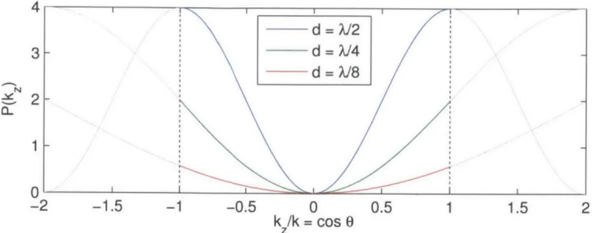
An illustration of the effect of element spacing on the power pattern is shown in Figure 2-2 for uniform linear arrays of fixed length L = 20A scanned to kzo = k/2 (at an angle of
300 from the broadside direction normal to the array). In each plot, a portion of imaginary
space is shown to highlight the grating lobe behavior. For d = A/4, the first main lobe
alias lies well outside the visible region and does not appear within the displayed range of
kz. At a spacing of d = A/2, we can see that the beam can be scanned nearly to the edge
of the visible region before the first grating lobe begins to appear at the opposite edge. In the case of d = A, an exact copy of the main lobe appears within V and we see that this is
unavoidable at any scan angle kzo.
As we see in Figure 2-2a, when d < 7r/k, Vo extends beyond the visible region. In this
case, it is possible to scan the main lobe entirely outside of real space. In the transmit case, this has the physical interpretation that the array is attempting to direct power into imaginary space, and as a consequence very little power will actually propagate away from the array. The receiving array has an analogous interpretation: it is attempting to focus on signals coming from imaginary space, thus causing any signal from real space to be combined incoherently.
With no apparent benefit gained from choosing a particularly small element spacing, conventional array design generally dictates that the spacing be set at or just slightly less than do = 7r/k = A/2. Based on this convention, a linear array with aperture length
2.1. LINEAR ARRAYS OF ISOTROPIC ELEMENTS 0 V. -10 - -20--30 --1 -0.5 0 k z/k = cos 0 0.5 1 1.5 2 (a) d=}= -1 -0.5 0 0.5 1 1.5 2 kz/k = cos 0 (b) d = = --1 -0.5 0 0.5 1 1.5 2 kz/k = cos 0 (c) d = A = 2k
Figure 2-2: Power patterns for L = 20A linear array scanned to ko = k/2. The edges of the visible region are marked with vertical dotted lines.
-401 -2 I ,~~1 -1.5 0 -10 c.N -40 -2 -1.5 0 101-c.N -20- -30--40' -2 -1.5 I
--I - - I -20--30-N = No = L/do. When the same aperture is filled uniformly with more than No elements, the resultant array is described as a dense array. As will be shown, while there is no benefit to using such an array with idealized components, a dense array has the potential to be useful for practical phased array implementation.
For our development, it is important to emphasize the distinction between the impacts of varying the array aperture size versus varying the number of array antennas, as these parameters are independently chosen in our architecture. To first order, the aperture size determines the fundamental pattern characteristics such as beamwidth and directivity. In a traditional array with element spacings near a half-wavelength, changing the aperture size is equivalent to changing the number of antennas. However, with the AE array architecture we focus on a fixed, but arbitrary array aperture within which the number of antennas is increased by reducing the element spacing throughout the aperture, resulting in a greater
2.2
Mutual Coupling
Physically, the array weights in (2.1) represent voltage or current excitations applied to the individual elements. For example, in an array of thin-wire dipoles, these weights are the currents across the terminals of the two dipole halves. Implicit in this expression for the beam pattern is the assumption of direct control over these terminal currents. This is known as the forced excitation model.
A more accurate representation of a practical array system is the free excitation model,
characterized by the equivalent circuit shown in Figure 2-3. In this model, the weights
{wn}
represent the complex voltages generated by individual sources, each with internal impedance Zo. The array is described as an N-port network with impedance matrix Z E CNxN such that v = Zi [37], where v and i are length-N vectors containing the voltages{vn}
and currents {in} at the terminals of the array elements. The terminal currents in Figure 2-3 are related to the weights w E CN according tow = Zoi + v = (ZoI + Z)i, (2.2)
where I is the N x N identity matrix. Defining the coupling matrix as C = (ZoI + Z)-,
such that i = Cw, the effects of the feed network and mutual coupling may be accounted for by replacing the wn in (2.1) with in =
Z4-1
CnmWin. The resultant beam pattern withmutual coupling is then
N-1 N-1
fMC(kz) = ZZ Cmwmeinkzd. (2.3)
n=O m=O
The model described above is commonly used in traditional mutual coupling analysis-see, e.g., [38]. We may obtain a useful form for the purpose of our analysis by exploiting certain structure in the coupling. In particular, it is useful to express (2.3) in terms of the
embedded element patterns, which are the patterns due to a unit excitation at a specified
element while in the presence of the remaining array elements. While these will vary among the elements near the edges of the array, most elements behave similarly to the elements of an infinite array. In the infinite array model, the physical coupling environment is constant for all elements and as such, the coupling matrix C has a Toeplitz structure, with identical entries along each diagonal cp = Cm+p,m. Thus, the complete coupling matrix may be represented by the set {cp}, which we refer to as the infinite array coupling coefficients.
2.2. MUTUAL COUPLING
I.
o414
z
C
4
WI zorV10
"1
V
1 I9I-i
)
VN.
*1
Z
Figure 2-3: Equivalent circuit diagram for the antenna array. The beamformer output is described by a set of voltage sources {w,}, each with internal impedance Zo. The mutual coupling among the array elements is modeled as a N-port network with impedance matrix
Z.
io
44Making the substitution p = n - m in (2.3), the beam pattern for the infinite array is f MC (k ) = Z :cpwmej(m+p)kzd m p = : wMejmk, d I p jpk d m p
f
(kz) fc(kz). (2.4)In (2.4), we have rewritten the free excitation beam pattern (2.3) as the product of the forced excitation beam patterns due to {Wm} and {cp 1}, the latter, which we refer to as the
coupling pattern of the array fc(kz). From (2.4), we can see that the coupling pattern is the
beam pattern of the array when a unit excitation is applied to the element located at the origin. Note that this is precisely the embedded pattern shared by all the array elements (up to a phase term). This useful factorization of the beam pattern allows for a convenient separation of the coupling effects from the simpler forced excitation relation used when mutual coupling is ignored.
2.3
Power Efficiency
Under perfect conditions, an array will radiate all the available power delivered by the source. When the power radiated by the array Prad is less than the incident power sent
from the source Pinc, the array is said to have a loss in the power efficiency
Prad (2.5)
Pinc
If the array is composed of lossless materials, efficiency loss is due to impedance mismatches between the source and the array elements. Since the impedance of each element is the ratio of the voltage to the current across the element terminals, mutual coupling causes these mismatches to vary with each particular array excitation.
For a particular choice of source excitations w, the power radiated by element n is
Re{i*vn}. The total power radiated is then N-1 Prad = Re{i*vn} n=O - Re{itv} = it Re{Z}i Swt (ZoI + Z) -t Re{Z}(ZoI + Z)-w. (2.6)
The power efficiency will be maximized when the array is perfectly impedance matched such that v = Zi = Zoi. Hence, the total available incident power can be deduced from
(2.6) by noting that Pin, = Prad when Z = ZoI, with the result
1
= w w. (2.7)
'fc - 4Zo
2.3. POWER EFFICIENCY
following expression for the array efficiency in terms of the array excitations:
wt(I - StS)w I ISwI12
whr1e- S , (2.8)
Chapter 3
Delta-Sigma Quantization for
Phased Arrays
In this chapter we consider the issue of pattern distortion caused by phase quantization in the excitation of phased arrays. Traditionally, the only recourse available for reducing this distortion has been to decrease the level of quantization error through the use of phase shifters with higher resolution, a primary driver of the high cost of phased arrays. The first of the two array designs proposed in this thesis employs an alternative approach for efficient quantization inspired by the Delta-Sigma modulation technique originally developed for use in analog-to-digital converters.
3.1
Traditional Delta-Sigma Quantization Concepts
In practice, the phases of the complex array weights are restricted to some finite set of quan-tized values defined by the resolution of the phase shifters used in the network connecting the array to the source. Phase shifters with M-bits of resolution can provide any of 2M
val-ues uniformly distributed over the range [0, 27). For a desired excitation w, = ae0-, the realized excitation is 7b = Q[w,] =
agej
n, where the quantization operatorQ
selects b,7such that the phase is the available value closest to 0,. Consequently, this adds undesired distortion to the far-field beam pattern.
The issue of phase quantization in the excitation of array elements draws a close anal-ogy to the difficulty that arises in the implementation of conventional analog-to-digital converters. At each sampling instance, the input signal xi is mapped to one of a number of discretized values yi. This introduces an additive error ej, as shown by the equivalent circuit in Figure 3-1. To keep distortion levels low in the output signal, the circuits in this type of converter require high-accuracy analog components.
3.1.1 Oversampling
Consider a signal bandlimited to 0 <
f
< fo sampled at frequencyf,.
Whenf,
is greater than the Nyquist frequency 2fo, the signal is said to be oversampled by a factor defined as the oversampling ratio (OSR)OSR = IS (3.1)