HAL Id: tel-00779488
https://tel.archives-ouvertes.fr/tel-00779488
Submitted on 22 Jan 2013
HAL is a multi-disciplinary open access archive for the deposit and dissemination of sci-entific research documents, whether they are pub-lished or not. The documents may come from teaching and research institutions in France or abroad, or from public or private research centers.
L’archive ouverte pluridisciplinaire HAL, est destinée au dépôt et à la diffusion de documents scientifiques de niveau recherche, publiés ou non, émanant des établissements d’enseignement et de recherche français ou étrangers, des laboratoires publics ou privés.
Arantxa Vilalta-Clemente
To cite this version:
Arantxa Vilalta-Clemente. Structure des Couches d’InN et d’alliages (In,Al)N. Science des matériaux [cond-mat.mtrl-sci]. Université de Caen, 2012. Français. �tel-00779488�
ECOLE DOCTORALE : Structure, information, matière et matériaux
THESE
présentée par
Arantxa VILALTA-CLEMENTE
et soutenue
Le 25 Avril 2012
En vue de l’obtention du
DOCTORAT de L’UNIVERSITE DE CAEN
Spécialité : Génie des matériaux
Arrêté du 07 août 2006
Structure des Couches d’InN et d’alliages (In,Al)N
JURY
Mr. Patriarche Gilles, Directeur de Recherche CNRS, LPN, Marcoussis, France, Rapporteur Mr. Vickridge Ian, Directeur de Recherche CNRS, INSP Paris, Rapporteur
Mr Giesen Christoph, Ingénieur Aixtron SE, Aachen, Germany
Mr. Grandjean Nicolas, Professeur Ecole Polytechnique de Lausanne, Switzerland Mr. Levalois Marc, Professeur Université de CAEN
Mr. Tuomisto Filip, Professeur Université Aalto, Finland
Mme Morales Magali, Maître de conférences HDR Université de CAEN, Co-directeur de thèse Mr. Ruterana Pierre, Directeur de Recherche CNRS, CIMAP, Directeur de thèse
"La vida és risc; l’aventura és novetat radical; la creació es produeix cada dia, quelcom absolutament nou i imprevisible"
Raimon Panikkar
“Life is risk, adventure is radical innovation; creation takes place everyday, something absolutely new and unpredictable"
Acknowledgments
uring many years I have made a long travel in the research world, and this part of the manuscript gives me the opportunity to express my thanks to many people that I have met along this journey until I wrote my PhD thesis.
First, I would like to thank my advisor, Pierre Ruterana for giving me the opportunity to join the RAINBOW Project at CIMAP laboratory in Caen and for his support, guidance and encouragement over the development of my PhD investigation, and especially for introducing me in the world of the dislocations and defects of the materials and for having his office door always open for me. I am very grateful to Magali Morales, my co-advisor, for her contribution and guidance to the RSM measurements and IBA analysis.
I convey my thanks to the members of the PhD committee: the President Prof. Marc Levalois (Université de Caen); the reviewers: Drs. Gilles Patriarche (LPN) and Ian Vickridge (INSP); examinators Prof. Nicolas Grandjean (EPFL), Prof. Filip Tuomisto (University Aalto) and Dr. Christoph Giesen (Aixtron); invited: Dr. Marie-Antoinette Di Forte-Poisson (Thales III-V Labs) and Prof. Evgenia Valcheva (University of Sofia) for having kindly accepted to judge my work, amidst their busy schedule. I greatly benefited from their constructive comments which greatly improved the manuscript.
I have to acknowledge, evidently, all the family of RAINBOW project: Professor, Supervisors, ESRs and ER for contributing with their talks during the numerous workshops and conferences that we attended together, the long discussions about the materials that we characterized and for the numerous hours that we enjoyed together in different countries and places.
D
Several collaborations have contributed to the InAlN and InN results in a significant way, and I had the opportunities of scientific visits which became a crucial point in my thesis and I would like to mention some of them. In particular, I would like to thank Marie-Antoinette Poisson (III-V Labs) for the MOVPE InAlN samples, and for her explanations on how this material is difficult to grow; Slawomir Kret (IFPAN) for the introduction to Optimas software and simulations; Evgenia Valcheva for the Raman measurements, Gilles Patriarche (LPN) for his critical and kind contribution of HAADF-TEM along with the important discussions on semiconductors materials and characterization; Ian Vickridge (INSP) for the measurements and discussions on IBA techniques.
For this work, the sample preparation was a crucial step for TEM observations, so I owe special thanks to Marie Pierre and Yadira for teaching me the preparation of the TEM samples and of course many thanks also to the growers (III-V lab, Aixtron, EPFL, TUB and UPM), who have provided me the samples without which I could not have been able to carry out this work.
I would always remember the nice moments I spent in CIMAP, my second home during all this time, and the friends I leave. I want to thank very specially Bertrand “ja ja”, for his patience and listening to all my questions, for his generosity and to encourage me in the research and of course: “je suis contente”. I thank my co-workers Geeta, Claire, Yi and Elodie for sharing different experiences during these years. I would like to thank Cédric, Michael and Stefan for lunch time and their patience with my French. I also enjoyed the companionship of the NIMPH group members at CIMAP and the coffee time with them.
Thanks to the Spanish Community: Diana, Elsa, Sheila, Luis and Western for the weekends and evenings; and French Community: Burcu, Olivier, Thomas, Delphine and Florent pour vos soirées.
I cannot forget my first stay abroad in Thessaloniki with another Marie Curie Project (SYNTORBMAG, Sept. 2007-Oct.2008). Thanks to Makis Angelakeris for giving me the opportunity to start as an ESR and to have the patience for my talks together with Kostas. Ευχαριστω Stefanos for teaching me the synthesis of nanoparticles and how a precursor or a different solvent can change their shape,
thank you also for the φρα̟ε µετριος µε γαλα. Eυχαριστίες to all the κορίτσια: Kathrin, Maya, Lata, Julita, Alkyoni, Aria, and Eleni for the time that we spent together and for encouragement to continue with the research.
I would like to thank especially the friends that I know from FiCMA group where I did my master: Cinta, Joan, Sandra, Òscar (you always will be with us), Montse, Isabel and Ana. Thanks for all the time that we spend together, for all the trips together and for your visits to me in Thessaloniki and Caen, and for the scientific discussions and long conversations by skype helping me to feel close to home. Thanks Sandra and Frida for the first six months that we were living together in Caen.
To my colleagues and friends at Servei de Recursos Científics i Tècnics (SRCiT) de Tarragona perque m’heu ajudat i m’heu donat ànims en totes les decisions que vaig pendre i prenc, mai podré oblidar el temps que vam treballar junts, gràcies Pepi, Lucia, Cristina, Carme, Ester, Francesc i Toni.
Naturally, I can not forget the chemistry group, for which we just celebrated our 20 years of existence, so thanks: Dolors, Angelina, Sílvia, Eva, David, xatos, xata and petits. I want to thank my friends Geni and Noèlia, amb vosaltres vaig començar a viure a Tarragona i en tot moment heu estat al meu costat, gràcies per les xerrades telefòniques, per tots els moments i experiències viscudes i que són molt difícils d’explicar en dues línies. También le quiero agradecer a Jose su confianza depositada desde que empecé a trabajar como técnica del AFM, y por su empuje constante para la investigación. My special thanks to all the friends and colleagues, whom I have met during this trip, and who, for small reason, kindly helped me to become the person and researcher I am now.
Thanks, finally, to my family, for dedicating so much time and effort in my education and for always standing by me, for their love, trust and support all the way. This is a small reward after so long time. And thanks to Στεφανος, for patiently listening to me, for keeping me strong, but most for all, for sharing many moments.
To my parents: Joan and Marina To my sisters and brother: Ruth, Nuria and Angel To my brother-in-law and sister-in-law: Patricio and Marta To my nieces and nephew: Marina, Leire, and Ignacio
Content
R
ésumé xviiL
ist of Abbreviations xxixI
ntroduction 1 Chapter1
III-Nitrides properties and applications 5 1.1 Brief history of nitrides 6 1.2 InN: Introduction and applications 91.3 InAlN: Introduction and applications 9 1.4 Structural properties 11
1.4.1 Crystalline structure 11
1.4.2 Polarity and piezoelectric properties 12
1.4.3 Substrates 14
1.4.3.1 Sapphire (Al2O3) 17
1.4.3.2 SiC 18
1.4.3.3 Si 18
1.4.4 Mosaic model 19
1.4.5 Strain and stress 20
1.4.5.1 Critical thickness 20 1.4.5.2 Residual stress 21 1.4.6 Structural defects 24 1.4.6.1 Point defects 25 1.4.6.2 Dislocations 25 1.4.6.3 Planar dislocations 27
1.5 InN and InAlN Growth 28
1.5.1 InN 28
1.5.2 InAlN 30
1.5.3 Growth modes 31
1.5.1.1 Frank- van der Merwe mode (FvdM) 31
1.5.1.2 Stranski-Krastanov mode (SK) 32
1.5.1.3 Volmer-Weber mode 32
1.6 A brief review of the optical properties of nitrides 32
1.7 Aim of this work 34
Chapter
2
Experimental Techniques 412.1 Growth techniques 42
2.1.1 Metal Organic Vapour Phase Epitaxy (MOVPE) 42
2.1.2 Molecular Beam Epitaxy (MBE) 43
2.1.3 Hydride Vapour Phase Epitaxy (HVPE) 44
2.2 Characterisation techniques 44
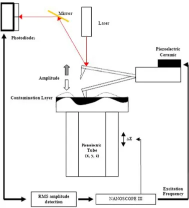
2.2.1 Atomic Force Microscopy (AFM) 44
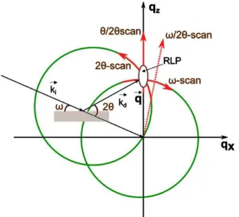
2.2.2 High Resolution X-Ray Diffraction (HRXRD) 46
2.2.2.1 Set up 46
2.2.2.2 Scans in reciprocal space 48
2.2.3 Electron Microscopy 51
2.2.3.1 Conventional Transmission Electron Microscope (TEM) 51
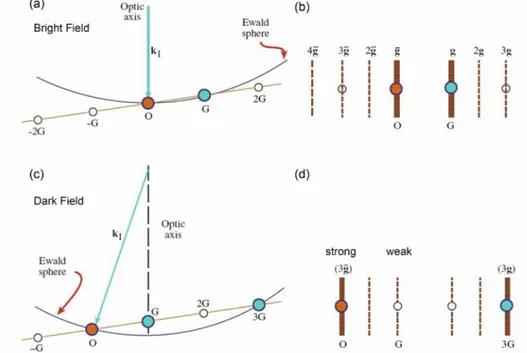
A) Bright field and dark field image 52
B) Two beam and weak beam conditions 53
2.2.3.2 Scanning TEM (STEM)/High Angle Annular Dark Field (HAADF) 56
2.2.3.3 Energy Dispersive Spectroscopy (EDS) 57
2.2.3.4 TEM sample preparation 57
2.2.4 Ion Beam Analysis (IBA) 59
2.2.4.1 Rutherford Backscattering Spectrometry (RBS) 60
2.2.4.2 Nuclear Analysis Reaction (NRA) 65
2.2.5 Raman Spectroscopy 65
References 68
Chapter
3
InN layers 713.1 Introduction 72
3.2 The samples 73
3.2.1 Raman and microstructure analysis 74
3.3 InN films grown by PA-MBE 82
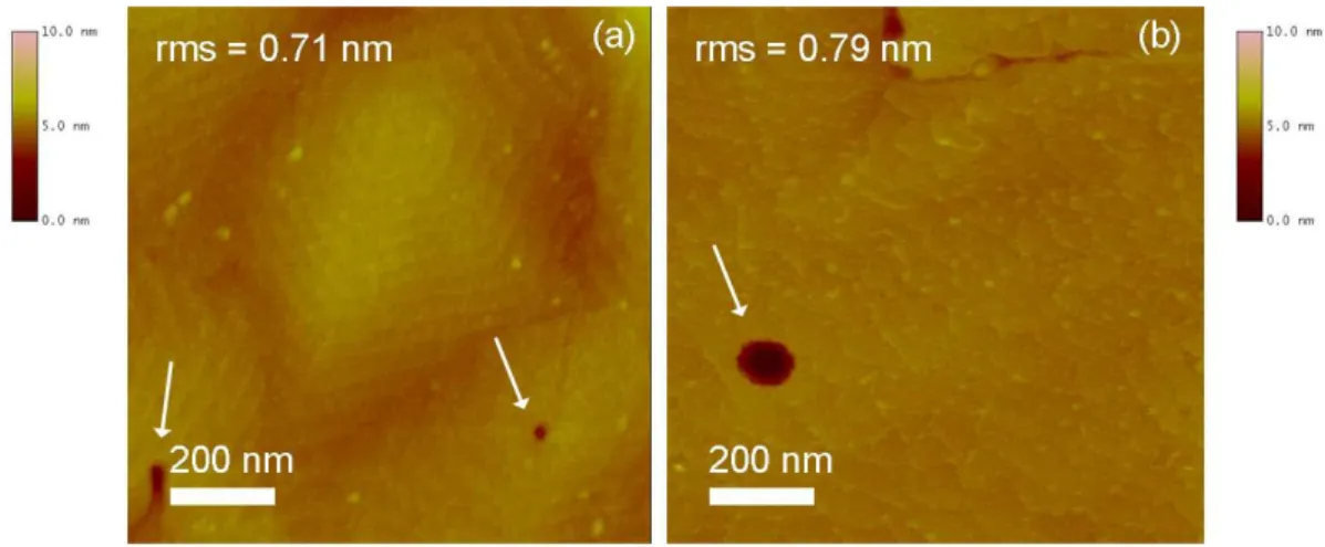
3.3.1 The surface morphology by AFM 83
3.3.2 Residual stress 86
3.3.3 The layers stoichiometry 91
3.3.4 Dislocation density 92
3.2.4.1 HRXRD: tilt and twist 92
3.2.4.2 Screw and edge dislocation density 103
3.4 Discussion 109
Chapter
4
InAlN heterostructures 1214.1 Introduction 122
4.2 Sample description 125
4.2.1 HEMT heterostructures 127
4.2.1.1 Cross section InAlN/AlN observations and surface morphology 127
4.2.1.2 Influence of the AlN interlayer 131
4.2.2 InAlN/GaN heterostructures 132
4.3 Composition analysis in InAlN/AlN/GaN and InAlN/GaN heterostructures 135
4.3.1 In content and strain analysis by HRXRD 135
4.3.2 In content and crystalline quality investigation by RBS/C 139
4.3.3 HAADF investigation and local In content by EDS 143
4.3.3.1 Elemental distribution in HEMT heterostructures 144
4.3.3.2 Structural degradation and chemical distribution 156
4.4 Discussion 160
References 167
C
onclusions andP
erspectives 171Résumé
tant donné que cette thèse est rédigée en anglais, vous trouverez ici un résumé en français des différents chapitres qui la composent. La structure de ce résumé est donc la même que celle du manuscrit, avec, premièrement, une introduction générale, suivi d’une courte chronologie concernant l’étude des nitrures et des applications associées ainsi que des techniques expérimentales mises en oeuvre. Les différents résultats sont ensuite exposés selon l’ordre des chapitres, pour finir par les conclusions et perspectives de ce travail.
I
I
I
ntroduction
Au cours des 50 dernières années, la recherche et les avancées technologiques dans les matériaux semi-conducteurs ont considérablement modifié notre mode de vie. Les outils tels que les ordinateurs personnels, les téléphones portables et les diodes électroluminescentes (LEDs) ne sont que quelques exemples de la multitude de dispositifs électroniques utilisés au quotidien. Les LEDs et diode laser à base de nitrures semiconducteurs sont le résultat d'une percée technologique qui a provoqué une révolution dans l'optoélectronique dès 1994.
Les nitrures d’éléments III: InN, GaN, AlN et leurs alliages se sont imposés pour le développement de dispositifs optoélectroniques de très bonne efficacité. La récente réévaluation de la bande interdite d’InN de 1.89 eV à seulement ~0.65 eV a permis d’envisager la production de dispositifs luminescents émettant dans
E
le rouge et le proche infrarouge (IR) et couvrir l’ensemble du spectre visible (de l’infrarouge à l’ultraviolet). Ces matériaux trouvent aussi des applications dans la réalisation de transistors à haute mobilité électronique (HEMTs). Bien évidemment, la production de dispositifs nitrures efficaces dépendra principalement de la qualité structurale des couches disponibles. La croissance des couches minces de nitrures pose encore de très nombreux problèmes. En effet, l’absence de substrats adaptés en paramètres de maille et/ou coefficients de dilatation thermique constitue un problème majeur pour la croissance d’hétérostructures de ses composés et de leurs alliages.
Au cours de ce travail, j’ai étudié des échantillons venant de trois techniques de croissance: épitaxie par jets moléculaires assistée par plasma (Plasma-Assisted Molecular Beam Epitaxy, PAMBE), épitaxie en phase vapeur à base d’hydrures (Hydride Vapour Phase Epitaxy, HVPE) et épitaxie en phase vapeur aux organométalliques (Metalorganic Vapour Phase Epitaxy, MOVPE). Dans le cas d'InN, la technique PAMBE a produit les couches de meilleure qualité réalisées à ce jour, avec cependant de faibles vitesses de croissance. La méthode MOVPE présente des avantages importants pour la fabrication de dispositifs commerciaux car elle permet des vitesses de croissance et de production élevées. Cependant, elle possède des limitations pour la croissance de l'InN, en effet, elle nécessite une température de croissance relativement élevée pour obtenir un craquage effectif de NH3.
Ce travail s’est inscrit dans le cadre du projet européen RAINBOW intitulé "High Quality Material and intrinsic Properties of InN and Indium rich Nitride Alloys". L’objectif scientifique de ce projet est d’obtenir des couches de semiconducteurs nitrures d’indium et leurs alliages de bonne qualité cristalline, et comprendre leurs mécanismes de croissance afin d’améliorer leurs propriétés opto- et micro- électroniques. Ma contribution à ce projet a été focalisée sur l’analyse détaillée de la structure d’InN et d’InAlN, en utilisant différentes techniques de caractérisation complémentaires. Il a été mené en étroite collaboration avec des partenaires qui faisaient la croissance des couches et ceux
qui fabriquaient les dispositifs, ceci dans le but d’aider à l’amélioration de la qualité des matériaux et les performances des dispositifs.
Le manuscrit est divisé en quatre chapitres:
Chapitre
1
1
1
III-Nitrures propriétés et applications
Le premier chapitre présente une courte chronologie de l’état de l'art dans les semiconducteurs nitrures et des applications de InN et InAlN. Après avoir décrit la principale phase dans laquelle ces matériaux cristallisent (structure wurtzite), nous nous sommes intéressée plus particulièrement aux caractéristiques structurales (polarisation spontanée et piézoélectrique, contraintes et déformations, épaisseur critique, défauts dans la structure wurtzite (défauts ponctuels, dislocations et fautes d’empilement) et aux propriétés optiques. Nous avons examiné plus particulièrement les problèmes liés au choix du substrat. Enfin, nous avons finalement discuté des diagrammes de croissance pour InN et InAlN.
Chapitre
2
2
2
Techniques expérimentales
Dans une première partie, nous avons décrit les trois techniques de croissance qui ont été employées par les différents collaborateurs. Les couches d’InAlN ont été réalisées par MOVPE dans deux entreprises, III-V labs (Marcoussis) et Aixtron (Allemagne), ainsi qu’à l’Ecole Polytechnique de Lausanne (EPFL-Lausanne). Les échantillons d'InN ont été élaborés par différentes méthodes de dépôt dans trois différent laboratoires: par MBE (Instituto de Sistemas Optoelectrónicos y Microtecnología à Universidad Politécnica de Madrid, ISOM-UPM), par MOVPE (Technische Universität Berlin-TUB) et par HVPE (EPFL).
La deuxième partie de ce chapitre est dédiée à la description des principaux équipements utilisés dans ce travail. Les morphologies de surface et la rugosité des InN et InAlN ont été caractérisées par la microscopie à force atomique (AFM).
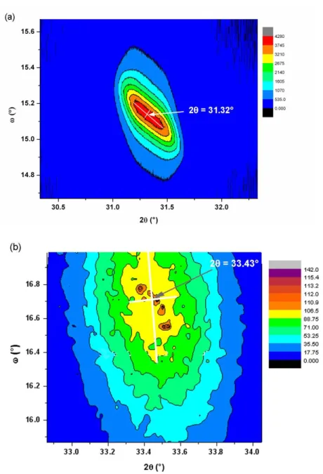
La diffraction de rayons X haute résolution (DRXHR) a permis de déterminer les paramètres de maille, et de connaître les contraintes et la composition en indium dans InAlN. En outre, la densité de dislocations a également été examinée par DRXHR à partir des mesures de l’inclinaison (tilt) et de torsion (twist).
La microscopie électronique en transmission a été utilisée pour la caractérisation des défauts cristallins en champs clair et sombre, ainsi qu'en faisceau faible qui permet d'optimiser le contraste pour une meilleure identification des défauts.
Par la suite, nous avons eu l'occasion d'utiliser, de façon extensive, la microscopie électronique en transmission à balayage en mode champ sombre annulaire à grand angle (HAADF-STEM). Cette technique présente un intérêt considérable car le contraste dans les images est sensible à la composition chimique locale.
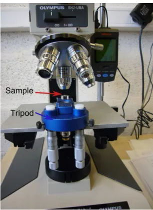
La microscopie électronique en transmission nécessite la préparation d’échantillons pour être transparents aux électrons. Nos lames minces ont été préparées en section transverse ou plane. Deux méthodes de préparation ont été utilisées: la méthode du tripode et l’amincissement mécanique.
Les méthodes d’analyses par faisceau d’ions (IBA) constituent un ensemble de techniques dérivées des interactions ion-matière. Dans ce travail, nous avons utilisé deux méthodes: la spectrométrie par rétrodiffusion de Rutherford (RBS) et l’analyse par réaction nucléaire (NRA). La RBS est une technique d’analyse des matériaux solides qui permet de séparer les éléments en fonction de leur masse atomique, d’obtenir des informations sur la composition chimique et les concentrations de chaque espèce, et de déterminer leur distribution en profondeur. La NRA est une variante de la RBS qui permet d'étudier les éléments légers, comme l’azote.
En plus des rayons X, nous avons utilisé la spectroscopie RAMAN pour accéder à la déformation dans les couches et déterminer la densité des porteurs résiduels dans les couches InN.
Chapitre
3
3
3
Couches d’InN
La première partie de ce chapitre a été utilisée pour comparer la microstructure des couches obtenus par les trois techniques de croissance: HVPE, MOVPE et MBE. Pour se faire, nous avons corrélé les résultats de spectroscopie RAMAN avec les analyses par microscopie électronique en transmission. Avec la spectroscopie Raman, les couches MOVPE-InN et MBE-InN ont une meilleure qualité cristalline que HVPE-InN. Les couches MOVPE sont caractérisées par un mode de croissance en îlots avec de nombreuses cavités au niveau des interfaces. Bien évidemment, cette structure est préjudiciable à la fabrication de dispositifs. Comme les couches MBE présentaient des surfaces planes et une microstructure uniforme, nous procédé à leur caractérisation détaillée. Un des buts était de corréler la morphologie de surface des échantillons et conditions de croissance (température, le rapport V/III, l’épaisseur des couches). Par microscopie à force atomique, nous avons mis en évidence que les échantillons fabriqués dans des conditions riches en indium avaient une rugosité plus faible que ceux riches en azote. Pour les échantillons produits à des températures de croissance plus basses (400 °C), la rugosité augmente rapidement. Nous avons observé que pour de meilleurs résultats, la croissance devait être faites autour du rapport V/III le plus proche possible de un, mais dans la région riche en indium à des températures d’environ 470 ° C.
Nous avons réalisé l’étude des contraintes dans ces couches MBE-InN. Pour ce faire, la diffraction des rayons X s’est révélée un outil particulièrement adapté; nous avons pu mettre en évidence une contrainte résiduelle de compression pour tous les échantillons déposés sur GaN/Al2O3, alors que pour les échantillons
déposés sur Si, nous avons une déformation en expansion lorsque la couche InN est déposée sur AlN/Si, alors qu'elle devient compressive sur GaN/AlN/Si. Après avoir comparé les résultats de la déformation de nos échantillons avec la littérature, on a déduit que des couches MBE-InN présentent deux composantes de déformation: l’une biaxiale et l’autre hydrostatique, cette dernière est souvent liée à la présence défauts ponctuels (donnée vérifiée par les analyses NRA et RBS).
Par la suite nous avons déterminé les densités de dislocations en comparant les résultats de DRXHR et les données obtenues par les analyses en MET. Il en découle que le pourcentage de dislocation c et a+c sont en faible proportion. Dans ces couches, les dislocations coin (type a) prédominent; et les résultats de MET sont conformes aux calculs DRXHR d'après le modèle mosaïque lorsque l'on utilise une petite taille de grains (≤90nm).
Chapitre
4
4
4
InAlN hétérostructures
Dans ce quatrième chapitre, nous avons caractérisé deux types d'hétérostructures: InAlN/AlN/GaN (avec une couche ultrafine d’AlN pour l’amélioration du gaz d’électrons à deux dimensions-2DEG) et InAlN/GaN.
Les couches ont été préparées par MOVPE dans différentes conditions de croissance (la température, le rapport V/III, des flux de gaz, etc..,) dans trois laboratoires (Aixtron, EPFL et III-Vlab). La croissance d'alliages d'InAlN est difficile à cause des grandes différences entre InN et AlN: paramètre de maille, énergies de liaison et températures de croissance. Son contrôle très précis est critique pour l'obtention de couches de bonne qualité. Par exemple, la croissance d'AlN requiert une haute température (>1000 °C), une basse pression, et un faible flux de NH3. Par contre, pour la croissance d'InN, il faudra une basse température
(~500 °C), une pression partielle élevée de NH3 et une pression total relativement
élevée pour optimiser l'incorporation d'In.
Dans une première partie, nous avons analysé l’influence de l’épaisseur de la couche intermédiaire d'AlN (hétérostructures InAlN/AlN/GaN) sur la structure de la couche d'InAlN avec AFM et MET. Dans cette étude il a été observé que l'épaisseur de la couche d'AlN a une influence sur les défauts dans InAlN et sa morphologie. Par exemple, une épaisseur d'AlN de 6.9 nm conduit à l'apparition d'une très forte densité de défauts en forme de V dans la couche d'InAlN. Donc, le contrôle exact de l'épaisseur de la couche AlN est un facteur important pour la qualité cristalline de l’InAlN. Dans le même sens, l'étude a été réalisée pour
montré que lorsque l'épaisseur devient trop grande, la crystallinité de l'alliage se dégradait très fortement.
Ce chapitre a aussi eu pour but une étude exhaustive de la composition en In dans ces hétérostructure InAlN/GaN et InAlN/AlN/GaN en utilisant DRXHR, RBS et EDS. Par DRXHR, nous avons pu déterminer à chaque fois une composition moyenne, qui dans les couches les plus minces correspondait parfaitement à la loi de Végard corrigé en accord avec les mesures RBS. Par microscopie analytique, on contaste des fluctuations locales qui s'amplifient avec l'augmentation de l'épaisseur de l'InAlN.
Enfin, un point importante dans ce chapitre (grâce à l’analyse EDS) est l'observation de la présence du Ga dans la plus part des couches intermédiaires d'AlN. De plus, dans certains échantillons, le Ga a même été incorporé dans toute la couche d'InAlN.
C
C
C
onclusions et
P
P
P
erspectives
Au cours de notre travail, cinq techniques complémentaires (AFM, IBA, Raman, MET, DRXHR) ont été utilisées pour la caractérisation des couches d’InN (UPM, TUB, EPFL) et des hétérostructures InAlN/GaN and InAlN/AlN/GaN (III-V Labs, Aixtron, EPFL) dans le but de contribuer à l’optimisation des procédés. Les principaux résultats sont résumés dans ce qui suit.
Les couches d’InN
Dans un premier temps, nous avons mis en évidence que les échantillons MBE-InN disposent de la meilleure qualité cristalline, avec des densités raisonnables de porteurs libres résiduels. Ensuite, leur morphologie, état de déformation et densités de dislocations traversantes (TD) ont été étudiées en fonction des conditions de croissance (rapport V/III, la vitesse de croissance, la température, les conditions de croissance riche en In ou N). Tous les échantillons présentent deux composantes de déformation: l’une biaxiale, l’autre
hydrostatique. Par ailleurs, deux tendances typiques ont été observées, dans des conditions de croissance riches en N: on aboutit à une croissance en 3D (rugosité rms ~7nm) et les plus grandes densités de porteurs libres (8 et 17 x 1018 cm-3). Sur
substrat silicium, cette croissance donne des couches aux contraintes résiduelles et densités de dislocation plus basses (1.8-3.2 x 1010 cm-2).
Concernant les échantillons déposés dans des conditions de croissance riches en In, une croissance avec marches atomique a été obtenue (rugosité rms <1 nm). Dans ce cas, nous avons pu mettre en évidence le rôle important de la température de croissance: à basse température (T = 400 ºC), la densité TDs mesurée est la plus forte (5.5 x 1010 cm-2) tout comme la densité de porteurs libres.
Pour le reste des échantillons (à une température située entre 420 et 480 °C), les densité des TDs étaient comparables (3.6-4.4 x 1010 cm-2) tout comme la
morphologie de surface (en 2D).
Les couches d’InAlN
En parallèle, nous avons étudié deux séries d’hétérostructures dont la croissance a été obtenue par MOVPE: InAlN/AlN/GaN/sapphire et InAlN/GaN.
Nous avons pu observer que lorsqu’on fait croître une couche intermédiaire AlN, on génère des défauts dans l’InAlN en forme de V (v-shape), leur densité augmente avec l’épaisseur de l’AlN. De plus, dans les échantillons où la couche intermédiaire AlN est la plus épaisse (3 et 6.9 nm), s'est formée une double couche, dont la partie la plus proche de l’interface est riche en Ga, indépendamment de la température de croissance ( 850 et 790 °C). Dans le cas où la croissance de la couche intermédiaire a été faite à 1200°C, cette couche intermédiaire était systématiquement riche en Ga avec une épaisseur entre 3 à 4.6 nm selon l'échantillon au lieu de 1 à 2nm qui était l'objectif de départ. Dans les hétérostructures déposées 790 °C, nous avons observé une forte concentration en Ga, environ 50 % dans la barrière InAlN. En accord avec la littérature, lorsque la couche intermédiaire était de AlGaN, la densité 2DEG (1.16-1.50 x 1013 cm-2) est
légèrement inférieure à celle obtenue avec une couche intermédiaire AlN (2.49-2.98 x 1013 cm-2).
Concernant les barrières InAlN les plus fines (tInAlN < 33 nm), les couches
montrent une bonne cristallinité par RBS avec χmin=7-30 % selon les conditions de
croissance. Lorsque les barrières deviennent épaisses (tInAlN > 90 nm), la RBS
montre une formation de deux couches avec une teneur en indium différente. La couche en surface d’InAlN a un χmin of 100 % indiquant qu’elle est polycristalline.
Cette dégradation progresse vers l’interface avec le GaN lorsque l’épaisseur de la barrière augmente.
Une analyse de la composition locale a ensuite permis d’expliquer cette dégradation structurale. En effet, nous avons trouvé des fluctuations de la composition locale à l’échelle du nanomètre dès l’interface avec le GaN. L’amplitude de cette fluctuation est faible à l’interface, elle augmente fortement vers la surface des barrières.
Suggestions pour compléter ce travail
Concernant la croissance de couches InN, ce travail a montré qu'il reste une marge importante d’amélioration de la qualité des matériaux. Une première suggestion serait de tester pour toutes le techniques étudiées: l’utilisation de substrats de GaN de polarité N dont certains auteurs ont montré qu'ils sont intéressants pour la croissance d’InN par MBE. De plus, les conditions de croissance riches en N devraient être évitées, car elles conduisent à des couches avec des densités de porteurs libres plus importantes. Les résultats obtenus avec des couches MBE-InN sont plutôt intéressants dans les conditions de croissance riches en In. On a pu observer une corrélation entre la densité de porteurs résiduels et les dislocations traversantes. Cepandant, la plus faible densité de porteurs obtenue reste encore assez élevée, il reste donc beaucoup de place pour une amélioration de la qualité du matériau. Pour ce faire, on peut suggérer les tâches suivantes:
♦ La croissance des échantillons étudiés s’est faite avec des variations de températures importantes (variations pouvant aller jusqu’à 50 °C pendant la croissance d'une couche). Il est évident qu’un contrôle plus précis de la stabilité de la température lors de la croissance serait la première étape à effectuer.
♦ On a vu que les échantillons que l’on a fait croître avec un rapport V/III = 0.8-0.88 montrent une croissance en 2D. Selon nos données, il est clair qu’une étude sur le vitesse de croissance pourrait apporter d’importantes améliorations.
Dans le cas des hétérostructures InAlN, trois conditions de croissance différentes ont été étudiées.
♦ A une température de dépôt plus basse, nous avons observé l’incorporation de Ga de ~ 43-50% à l’intérieur de l’InAlN, et ces échantillons présentent une bonne qualité cristalline en RBS. De telles conditions devraient être davantage explorées par la fabrication de dispositifs et la caractérisation afin de connaître les performances de façon précise.
♦ Lorsqu’on a fait croître une couche intermédiaire AlN à 1200 °C et V/III = 2200, le Ga s’est incorporé à l’AlN et aucun défaut en forme de V n’a été observé dans la couche InAlN. Ce résultat pourrait contribuer à la croissance d’hétérostructures avec une densité de défauts réduite. Par exemple, il serait intéressant de tester la croissance d’une double couche intermédiaire AlGaN/AlN. ♦ Dans tous les cas, l’uniformité de l’InAlN nécessite encore une recherche approfondie.
List of abbreviations
2DEG Two dimensional electron gas
αtwist Twist angle
αtilt Tilt angle
0 0, c
a unstrained lattice parameters
af Lattice parameter film
as Lattice parameter substrate
AECi Thales samples
AFM Atomic Force Microscopy
Aiii EPFL samples
Aixii Aixtron samples
b Burger vector b dilatation coefficients BF Bright field c Lattice parameter Cij Stiffness coefficients d0 grain diameter ∆ω Raman Shift
DBR Distributed Bragg Reflectors
DF Dark field
eij piezoelectric tensor coefficients
∞
ε
high-frequency dielectric constantεxx in-plane strain tensor
E Young modulus
EDS Energy dispersive spectroscopy
ECCI Electron channelling contrast imaging
φ azimuthal angle rotation
Φ Flux
fm misfit parameter
FvdM Frank-van der Merwe mode
FWHM Full width at half maximum
GB grain boundaries
HAADF High Angle Annular Dark Field
HEMT High Electron Mobility Transistors
HFET Heterojunctions Field Effect Tansistors
HRXRD High Resolution x-Ray Diffraction
HVPE Hydride Vapour Phase Epitaxy
Ix and Iref Intensity in an area unknown and know, respectively
IBA Ion Beam Analysis
IDB inversion domain boundary
IR Infrared
KH Hydrostatic linear pressure
L║ Lateral coherence length
L⊥ Vertical length
LED Light Emitting diode
µe Electron mobility
m* effective electron mass
MBE Molecular Beam Epiatxy
MOVPE Metalorganic Vapour Phase Epitaxy
ns Sheet carrier density
N concentration point defects
Nedge Dislocations with edge component
Nm concentration of lattice sites of the host matrix
NRA Nuclear Reaction Analysis
PAMBE Plasma Assisted Molecular Beam Epitaxy
PIPS Precision Ion Polishing System
PLD Pulsed Laser Deposition
Ppz Piezoelectric polarization
Psp Spontaneous polarization
rh covalent tetrahedral radius
rms root mean square
rs radius of solute atoms
RB Biaxial relation coefficient
RH Hydrostatic relation coefficient
Rs Sheet resistance
RBS Rutherford Backscattering Spectroscopy
RC Rocking curve
RHEED Reflection high energy electron diffraction
RLP Reciprocal lattice point
RSM Reciprocal space map
σkl stress tensor component
SAED Selected area electron diffraction
SF stacking faults
SK Stranski-Krastanov mode
STM Scanning tunnelling microscope
SEM Scanning electron microscopy
tAlN Thickness AlN
tc Critical thickness
tInAlN Thickness InAlN
TD Threading dislocation
TEM Transmission Electron Microscopy
TMA Trimethylaluminium
TMG Trimethylgallium
UHV Ultrahigh vacuum
UV Ultraviolet
V/III Ratio of the NH3 molar versus group III molar flow
VCSELS Vertical Cavity surface Emitting Lasers
WBDF Weak Beam Dark Field
χ tilt angle rotation
χmin minimum yield
XRD x-Ray Diffraction
Introduction
esearch and technological advancements in electronic materials have modified, in the last 50 years, our views, our attitudes and our way of living. Tools and gadgets like personal computers, mobile phones and Light Emitting Diodes (LEDs) are just some examples of the vast number of electronic devices. In this context, the nitride based LEDs and laser diode are clear examples: the blue light was the result of a technological breakthrough in 1994 and caused a revolution in optoelectronics.
Group-III nitride semiconductors InN, GaN, AlN and their alloys represent a unique materials family for the development and mass production of numerous electronic and optoelectronic devices. The recent revision of the InN band gap, down to only ~ 0.65 eV, allows the development of LEDs for the red and near-infrared spectral region and carries an important opportunity for covering the whole visible and UV spectral range using one family of compounds (group-III nitrides). Furthermore, such materials find applications in electronic devices like high electron mobility transistors (HEMTs). The performance of III-nitride devices depends critically on their structural quality. A related important issue for the growth of InN and In-rich alloys is the large lattice mismatches and thermal expansion coefficient with the available substrates (sapphire, Si, SiC) or even bulk GaN. As a consequence, thin epitaxial films usually contain a high density of structural defects which are detrimental to their physical properties. Suitable growth methods to reduce the threading dislocation density in InN materials have to be developed in order to improve the crystalline quality of the InN towards the fabrication of high efficiency devices, like solar cells or light emitters.
R
R
R
This work has been investigated three growth techniques: Plasma Assisted Molecular Beam Epitaxy (PAMBE), Hydride Vapour Phase Epitaxy (HVPE) and Metalorganic Vapour Phase Epitaxy (MOVPE). While PAMBE has produced the highest quality InN achieved so far, growth rates are typically lower than in MOVPE. The latter method has significant advantages for commercial device fabrication since it enables high growth rates and high volume production, but it also has some limitations as MOVPE requires relatively high growth temperature to thermally crack NH3, which is a particular challenge in the case of InN growth.
Indeed, thick InN layers are needed and HVPE is a most appropriate technique for this purpose. Two of the key objectives for the epitaxial growth development are the reduction of dislocation density and impurity concentrations in InN and its alloys and to realize high-quality In-rich alloys.
This work was carried out within the ‘RAINBOW ITN’ European project with the title “High quality Material and intrinsic Properties of InN and indium rich Nitride Alloys”. This thesis results from a detailed structural characterization of InN and InAlN heterostructures, using a number of complementary methods in close collaboration with the growers and device makers, with the aim of helping towards the improvement of the materials quality and device performances. Some of the results included in this manuscript have been obtained in collaboration with the other RAINBOW partners.
The manuscript is divided into four chapters. In the first Chapter, we present a brief history of the III-nitrides semiconductors and the applications of InN and InAlN. We describe the basic properties of wurtzite nitride semiconductors: residual strain, polarity, etc,... We discuss more specifically the problem for the choice of substrate and the structural defects in these materials. Finally, we present growth diagrams for InN and InAlN heterostructures as found in the literature.
In the second Chapter, a short description of the growth methods is reviewed; the characterization techniques employed in this work are also presented.
In the third Chapter the results of our detailed investigation of the InN layers are discussed. First, we compare the InN grown by the three different techniques:
PAMBE, HVPE and MOVPE and the rest of the chapter is focused on MBE-InN samples which are previously shown to have the best quality. The InN layers surface was analysed with atomic force microscopy (AFM). The residual strain of these layers was determined by high resolution x-ray diffraction (HRXRD). As already reported in GaN, the presence of a hydrostatic strain component in these InN layers is correlated to excess of nitrogen as shown by nuclear reaction analysis (NRA) and Rutherford backscattering spectroscopy (RBS). The determination and observations of dislocation densities by HRXRD and transmission electron microscopy (TEM) are also discussed. As would be expected due to large lattice mismatch between InN and the used substrates/templates, the a- edge type threading dislocations are predominant, while a lower percentage of mixed type dislocations is observed.
In the fourth Chapter the In composition of InAlN/GaN and InAlN/AlN/GaN is studied using HRXRD mapping, RBS and EDS, as well as high angle annular dark field imaging (HAADF). The potential of these techniques for the analysis of composition in inhomogeneous or heterogeneous layer systems as well as compositional fluctuations is demonstrated. The important finding in this chapter is the non intentional gallium incorporation in the AlN interlayer and for some samples it was even seen to be present all over the InAlN barrier.
In the end, the results of this work are summarized and an outlook to future work is given.
Chapter
1
III-Nitrides properties and applications
1.1 Brief history of nitrides
1.2 InN: Introduction and applications 1.3 InAlN: Introduction and applications 1.4 Structural properties
1.4.1 Crystalline structure
1.4.2 Polarity and piezoelectric properties 1.4.3 Substrates
1.4.3.1 Sapphire (Al2O3)
1.4.3.2 SiC 1.4.3.3 Si 1.4.4 Mosaic model 1.4.5 Strain and stress
1.4.5.1 Critical thickness 1.4.5.2 Residual stress 1.4.6 Structural defects 1.4.6.1 Point defects 1.4.6.2 Dislocations 1.4.6.3 Planar defects 1.5 InN and InAlN Growth 1.5.1 InN
1.5.2 InAlN
1.5.3 Growth modes
1.5.3.1 Frank- van der Merwe mode (FvdM) 1.5.3.2 Stranski-Krastanov mode (SK) 1.5.3.3 Volmer-Weber mode
1.6 A brief review of the optical properties of nitrides 1.7 Aim of this work
ince the dawn of civilization, the human being tried to understand and use the phenomena related to light. People had constantly wondered how to illuminate the night until they discovered with the use of fire. For the two last centuries, the lighting technology has taken more and more room and nowadays this field is one of the most interesting sectors of optical technologies.
The development of semiconductors has been crucial for technological applications. For last years, the research and applications of the III-nitride semiconductors have been highly extensive for materials without native substrates. Indeed, their synthesis for even better performances is still a challenge as the structural defects generated in the epitaxial growth are responsible for the low efficiency of the devices. The objective of this chapter is to present the structural properties of InN and InAlN compounds which are at the basis of this work.
1.1
Brief history of nitrides
Historically, the most important periods of Humanity have been designated as the different types of materials. Thus, Stone Age ranges from the Lower Paleolithic Period, about 2.5 million years to the Neolithic; Bronze Age begins around 3000 years BC, and from 1500 years BC until the Roman Period is the Iron Age. When, in the mid-seventies of last century, the number of publications on semiconductors materials exceeded at on steel, some historians began to call the period as the “Age of Semiconductors”. This strong growth is still underway until today, and semiconductors have led to a revolution, at least, comparable to that produced by the steam engine. Today, semiconductors based electronics has a clear impact on everyday life, at our work and in our home.
Group III-Nitrides (GaN, AlN, InN and their alloys) have remarkable properties, the first is their direct bandgap spanning from 0.65 eV (InN) to 6.2 eV (AlN) at room temperature, which should allow emission and detection of wavelengths ranging from infrared to deep ultraviolet. Other properties such as their high thermal and mechanical stability, large piezoelectric constants, or
S
electronic and optoelectronic devices able to operate at high temperature, high frequency and high power densities.
Among this III-nitride family, GaN is the compound that has been most investigated in the literature. The first report of III-nitride synthesis was in 1938 by Juza et al.1 for GaN and InN crystals. Then 30 years later, Maruska et al.2 grew GaN
layers by vapour phase deposition on sapphire substrates and measured its bandgap at 3.39 eV. Epitaxial layers were also reportd in the late 1960s using hydride vapour phase epitaxy (HVPE). In 1971, Pankove et al.3 reported the first
blue GaN-based diode consisting of a metal/insulating device. However most of this early research was eventually abandoned due to the high defect density and poor surface morphology of the available heteroepitaxial films. These problems began to be overcome in the mid-1980s and good quality of GaN thin films were obtained in 1986 by Amano et al.4 with the optimized two steps growth method
using metal organic vapour phase epitaxy (MOVPE). In this procedure, a thin AlN buffer layer was first grown on sapphire at low temperature (~600 °C), followed by GaN layer growth at a higher temperature (~1040 °C). The AlN buffer provided high density nucleation centers and promoted the lateral growth of the main layer, resulting in better quality of GaN thin films.4 Later, Nakamura5 reported that a
GaN buffer layer had a similar effect.
III-nitrides research increased in 1990s when Nakamura et al.6 working for
the Japanese company Nichia, announced the first blue light emitting diode (LED) based on GaN and InxGa1-xN.6,7 After that the progress of manufacturing devices
based on III-group nitrides was accelerated. In 2002, Nichia announced the development of high power InGaN LED’s for white, blue and green light emission with expected lifetime of 100000h. From the heterostructure LED and laser diode up to high electron mobility transistor (HEMT), all devices are now investigated using the nitride compounds and alloys.
In the early 1990s, it was discovered also that the III-nitride material exhibit strain induced and spontaneous piezoelectric polarization effects, leading to the demonstration of the two-dimensional electron gas (2DEG) at an AlxGa1-xN/GaN,
In 2001, Kuzmík10 proposed the use of the ternary InAlN in order to replace
AlGaN and improve the reliability of HEMTs. Indeed, InAlN/GaN systems have many predicted advantages over AlGaN/GaN heterostructures, in particular, by changing the Al to In ratio, the strain can be varied, while maintaining high electron sheet density, and devices degradation due to strain relaxation observed in AlGaN/GaN HEMTs can be reduced. The strain can be completely eliminated by growing InAlN/GaN lattice matched heterostructures. Many more details can be found in the reviews by Jan et al.11, Bhuiyan et al.12, and Vurgaftman et al.13
There are two fundamental reasons to choose the III-nitride system for light sources. First, as mentioned above, their direct band gap covers the entire visible spectrum from the UV to the IR. This is in a contrast to the (Ga,Al)As based LEDs (1.5–2.2 eV) or (Al,Ga,In)P based LEDs (1.3–2.5 eV) that cover only the IR to yellow region (Fig 1.1). The other advantage of the III-nitride semiconductors is their strong chemical bond, which makes them very stable and resistant to degradation under high electric currents and high temperatures.
Fig 1.1 Room temperature bandgap energy versus lattice constant of the nitrides and other
common semiconductors.14
However, despite intense research efforts worldwide, there still remains a strong need to improve the nitride based devices quality. In particular, in contrast
of suitable substrates leading to strong built-in strains and to the formation of cracks or dislocations detrimental for optical and electrical properties.
1.2
InN: Introduction and applications
Research on the growth and characterization of InN has increased tremendously in last years, mainly, due the recent redefinition of its band gap at 0.65 eV, in contrast to the earlier admitted value of 1.89 eV.15 The controversy
associated with the discovery of its narrow band gap has led to intense research efforts.15,16 Several reports have shown since that oxygen incorporation
(oxynitride) was one of the reasons for the earlier measured bandgap.17,18 It
became then very interesting to explore the AlN-GaN-InN alloy system for device applications in solid-state lighting, spintronics, and terahertz devices. Indeed InN is a key elemental in InGaN based LED as it exhibits smallest effective mass, the largest mobility and highest peak and saturation velocities of the III-nitrides.19 It
was also reported that InN rich alloys could be resistant to radiation damage20 and
therefore be used in a variety of device applications (including high efficiency multi-junction solar cells,21 high-brightness light emitting diodes22 and high
electron mobility transistors,10...).
Until now, integration of InN into device applications has been limited by a number of growth difficulties:
- low dissociation temperature
- high equilibrium vapor pressure of nitrogen molecules - lack of suitable substrate material for InN
1.3
InAlN: Introduction and applications
InAlN is the least characterised of the ternary nitride alloys: much less is known about its properties, compared to AlGaN and InGaN, due to its unstable growth conditions. The attractive features of InAlN are the wide bandgap range from 0.65 eV to 6.2 eV and the lattice matching of In0.18Al0.82N to GaN. This lattice
matched alloy has a large refractive index contrast to GaN and a direct band gap around 5 eV, which is larger than that of GaN (3.5 eV).
In contrast to other heterojunctions field effect transistors (HFETs) fabricated from the conventional cubic III-V semiconductors, the band gap discontinuities and polarization effects in nitride allow the HFETs without the need to dope the barrier. In this instance, the two dimensional electron gas (2DEG) from which originates the name of such devices (high electron mobility transistor or HEMT) is due to polarization and piezoelectric fields. However, in theses heterostructures, the lattice mismatch between AlGaN and GaN results in strain causing device degradation through defect generation. The possibility of growing lattice-matched InAlN/GaN removes the strain induced degradation of GaN-based HEMTs and piezo-polarization, potentially improving the heterostrucure stability. InAlN/GaN HEMTs exhibit a high 2DEG density (ns), together with
good mobility (µe) and low sheet resistance (Rs), solely due to spontaneous
polarization effects.23 Such devices show high temperature stability, and the
inclusion of an AlN ultrathin interlayer was shown to improve the 2DEG mobility.10 In such a device, (Fig 1.2), the current between drain (D) and source (S)
is controlled by the voltage on the gate contact (G), it flows through an ultra thin channel defined by the two dimensional electrons gas distribution.24
Apart from HEMTs, InAlN ultrathin layers are used in distributed Bragg reflectors (DBRs)25,26 such heterostructures are essential building blocks for
advanced optoelectronic devices (i.e. vertical cavity surface emitting lasers (VCSELS)). They consist in multilayer structures exhibiting a high reflectivity around a desired wavelength. In this instance, the InAlN lattice-matched DBRs prevents cracking.27 Other applications of InAlN consist in realization of
prototypes such as thermoelectric device,28 and ultraviolet photodiode.29
1.4 Structural properties
1.4.1 Crystalline structure
Group III-V nitrides (GaN, AlN, InN and their alloys) may take three crystalline structures: the wurtzite, zincblende and rock salt.30 For these nitrides
semiconductors (GaN, AlN, InN), the most stable structure is the wurtzite structure (space group P63mc) with four atoms per unit cell. The metal (Ga, Al or
In) element is surrounded by four nitrogen atoms, at the edges of a tetrahedron, this makes two translated compact hexagonal (HCP-hexagonal close packed) structures, which project along the [1120] direction as an ABAB layered structure, where A, and B form III-N pairs (Fig 1.3).
Fig 1.3 Schematic illustration of wurtzite structure.
In this structure, the bond length along the [0001] direction between N and the metal atoms is larger than the three other bonds of the basic tetrahedron, and its length as related to the c parameter is named u. This parameter is different for each compound. Taking an appropriate origin, the atoms inside the unit cell are then located at (1/3, 2/3, 0) and (2/3, 1/3, ½) (group III) and (1/3, 2/3, u) and (2/3, 1/3, ½+u) N.
1.4.2 Polarity and piezoelectric properties
Conventionally, the [0001] axis is defined as the direction which connects the metal to the N atoms, and if the crystals is cut along the A-B bond, as can be seen in Fig 1.3, the (0001) surface will be terminated by III atoms type, whereas the (0001) surface will be only populated by N atoms: the <0001> and <0001> directions correspond to III and V polar directions, respectively. One of the consequences of this polarity is a spontaneous polarization (Psp) which may take
place at interfaces. In addition to this Psp, the III-nitrides show a large piezoelectric
(Ppz) response to elastic strain. This results in a piezoelectric polarization when
their heterostructures are submitted to strain. The nitrides having different lattice parameters, their epitaxial heterostructures are either under tensile or compressive strain. At the interface of the heterostructures, the total polarization is then the sum of the spontaneous polarization due to the net difference of charges along the
c axis and of the strain induced piezoelectric polarization.
pz sp Total P P P r r r + = (1.1)
Table 1.1 lists the spontaneous and piezoelectric polarization of group III nitrides. As can be seen, the Psp of the III-nitrides is negative. In a theoretical
study, Bernardini et al.31 reported a strong nonlinear dependence of spontaneous
polarization on composition in chemically disordered alloys. Assuming that ternary nitride alloys have random microscopic structure, the same authors
expressed the piezoelectric parameter to second order in the composition parameter x as 32
Psp (InxAl1-xN) = -0.090 (1-x) – 0.042 x + 0.071 x (1-x) (1.2)
for the InxAl1-xN compounds C/m2. The first two terms are the usual linear
interpolation parameters between the binary compounds, and the third term is the so called bowing parameter.
Table 1.1 Spontaneous (Psp)32 and piezoelectric (Ppz)32 polarization for the group III nitrides,
piezoelectric tensor coefficients30 and stiffness coefficients.
Material GaN AlN InN
Psp (C/m2) -0.034 -0.90 -0.042 Ppz (C/m2) 1.8765 -3.1963 0.4448 e33(C/m2) 0.73 1.46 0.97 e31(C/m2) 0.49 0.60 0.57 C11 367 33 411 30 223 33 C12 135 41 149 30 115 33 C13 103 41 99 30 92 33 C33 405 41 389 30 224 33
For biaxial strained III-V nitride epitaxial layers grown in the (0001) orientation, the piezoelectric polarization occurring along the <0001> direction is given by:34 − = 33 13 33 31 , 2 C C e e Ppzz
ε
xx (1.3)where C13 and C33 are the stiffness elastic coefficients of the film, related to
tensor coefficients30 (Table 1.1) and εxx corresponds to the in-plane strain tensor
components, which is defined as
film film subtrate xx a a a − =
ε
(1.4)Applying the numbers in Table 1.1 to the case of InxAl1-xN grown on GaN,
it can be seen that Ppz (equation 1.3) is positive for compressive strain and negative
for tensile strain (as example: for In content 0.1 the Ppz is 0.030 C/m2, when xIn=
0.18 the Ppz=0 C/m2 and xIn=0.3 then the Ppz = -0.07 C/m2).
The polarization related properties are obviously important for devices because the electric fields influence the shape of the band edges and the carrier distribution inside nitride-based heterostructures. As was reported many times, spontaneous and piezoelectric polarization can influence the radiative recombination in light-emitting devices as well as the electrical properties in transistors.35
1.4.3 Substrates
As no bulk nitride substrates are commonly available in the nature, III-nitrides growth has been performed on a number of different substrates and crystal orientations. Growing heteroepitaxially requires the choice of a substrate with a surface template that matches the crystal symmetry of the desired material. The lattice mismatch between the substrate and the film leads to the generation of misfit dislocations at the interfaces in order to release the mismatch. Unfortunately the relaxation is never completely confined inside the interface and the dislocations usually propagate inside the interfacial layer. During such heteroepitaxial growth, not only the lattice parameters difference plays an important role, but also it is necessary to manage the thermal behaviour of the substrate and the epitaxial layers. Indeed at cooling down from the growth temperature, the substrate and film will relax in significantly different way
the investigated nitride layers were grown on [0001]-sapphire and Si substrates. As can see in Table 1.2, the lattice parameters, mismatch and thermal expansion coefficients are quite different between the nitrides and the used substrates. Therefore, one expects, if no special care is taken, the generation of large defect densities following heteroepitaxy of nitride layers on these substrates.
The main criteria for the substrate choice is that the substrate has a low lattice mismatch this is measured by the misfit parameter (fm) defined as
substrate film substrate m a a a f = − (1.5)
and asubstrate and afilm are the lattice constant for the substrate and the film,
respectively (Table 1.2).
Table 1.2 Parameters of III-V nitrides and substrates.
Material GaN AlN InN Al2O3 SiC Si
Structure Wurtzite Wurtzite Wurtzite Rhombohedral Wurtzite Cubic (111)
a 3.185 36 3.111 37 3.5378 38 4.765 39 3.0806 39 Lattice constant c 5.188 36 4.98 37 5.7033 38 12.982 39 15.1173 39 a = b = c = 5.431 39 Mismatch to GaN (%) 0 ~ 2.3 ~ -11 ~ 16 ~ -3.1 ~ 21 Mismatch to InN (%) ~ 11 ~ 13.7 0 ~ 29.2 ~ 14.8 ~ -7.8 ║ a-axis 3.17 4.2 3.09 5.0 4.3 Thermal expansion (10-6K-1)40,41 ║ c-axis 5.59 5.3 2.79 9.03 4.7 3.59
If the film consists on an alloy, such as InxAl1-XN grown on GaN, its lattice
constant depend on the composition x. Assuming that Vegard’s law is valid, the lattice constants of the films are given by42
a (InxAl1-xN) = x a (InN) + (1-x) a (AlN) (1.6)
c (InxAl1-xN) = x c (InN) + (1-x) c (AlN) (1.7)
Although its strict validity is under constant questioning, Dridi et al.43,
using first principle calculations, reported that the Vegard’s law holds for AlGaN (both lattice constants) and the a-lattice constant for InGaN and InAlN. The authors predicted a small deviation from Vegard’s law for the c-lattice parameter of the latter alloys. More recently, Darackchieva et al.44 used the ab initio program
VASP45 which uses the generalized gradient approximation and reported for
InAlN, that both a-and c-lattice parameters exhibit essentially a linear dependence on the In composition with very small deviations from Vegard’s rule. They concluded that even such small deviations could have influence on the strain calculations as carried from HRXRD and Raman data. They proposed the following equation for a and c:
ξ
( )
x =xξ( ) (
InN + 1−x) (
ξ AlN)
−δξx(
1−x)
and ξ =a,c (1.8) where δa = 0.0412 ± 0.0039 Å and δc = -0.060 ± 0.010 Å are the correspondingdeviation values respectively for the a- and c-cell parameters.
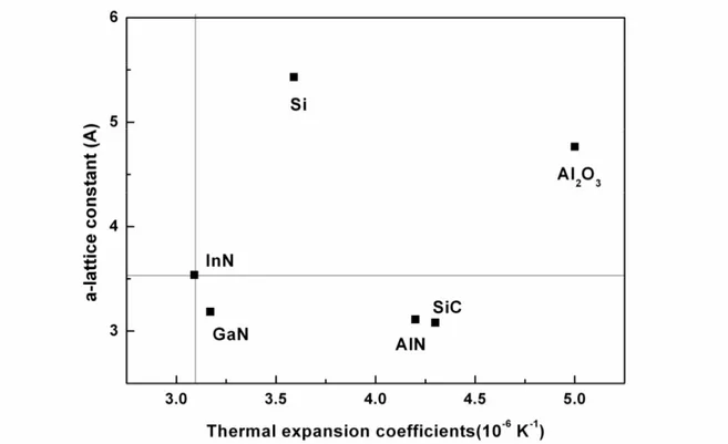
Fig 1.4 shows the lattice constants and thermal expansion coefficients for common substrates and III-N semiconductors. The plot gives an indication of how various substrates match indium nitride in terms of lattice constant and thermal expansion coefficient. It is interesting to note that the most common III-N substrate, sapphire, has the worst lattice and thermal expansion match to InN, as well as for the other nitrides (AlN, GaN). The use of sapphire substrates for the growth of nitride layers appears to have only been possible when the use of buffer layers was discovered.46
Fig 1.4 The a-plane lattice constant and a-plane thermal expansion coefficients for common indium nitride substrates and III-N semiconductors.
1.4.3.1 Sapphire (Al
2O
3)
Sapphire is the most extensively substrate used for the epitaxial growth III-nitrides although it has large lattice and thermal expansion match to III-nitrides Several orientations, such as c-(0001), a-(1120), m-(1100) and r-(1102), have been used for nitride. In this work, the investigated InN layers were growth on c-orientation. Usually, the InN is grown on top of a GaN/c-Al2O3, in this instance,
the unit cell of GaN is rotated by 30° around the c-axis with respect to the sapphire unit cell (Fig 1.5) and the lattice mismatch is ~ 16 % (Table 1.2) whereas for the non rotated GaN on sapphire is about 32 %.39 In fact, this rotation not only permits to
decrease the lattice mismatch between sapphire and GaN, but it also allows the alignment between the oxygen and III-element sub-lattices of the two materials.47
In this instance, the mismatch between sapphire and GaN lattice parameters is thus calculated using the following equation:
substrate GaN substrate m a a a f 3 3 − = (1.9)
If InN is grown directly on sapphire, two kinds of in-plane rotated domains can be observed with epitaxial relationships of [1010]InN//[1120]Al2O3 and
] 0 2 11
[ InN//[1120]Al2O3 where the lattice mismatch are 29.2 % and -25.4 %,
respectively.48
Fig 1.5 Schematic diagram of the plane crystal structure for a III-N/sapphire with the two atomic
arrangement. The blue atom is oxygen and the green atom is the III-element.49
1.4.3.2 SiC
Recently,50 InN epitaxial films were grown by PA-MBE at 450 °C on 4H-
and 6H-SiC substrates using low-temperature InN nucleation layers. It was shown that InN films grown under the In-rich regime show improved crystal quality, surface morphology, and optical properties. Photoluminescence measurements showed emission up to room temperature; the deduced band gap values as low as 0.64 eV at T = 10 K, and carrier concentrations were of the order of 8 × 1017cm−3.
1.4.3.3 Si
The interest of using Si as a substrate for nitride growth includes the crystalline quality and low cost, as well its highly dominant technological applications in the microelectronic field. Since Si has a diamond structure, the (111) Si substrates are usually used for GaN epitaxy. Silicon is also an alternative substrate for InN growth. Indeed, the lattice mismatch between InN/Si(111) is ~8 %, which is smaller than InN/Al2O3, and the low cost substrate as well as