HAL Id: hal-02998007
https://hal.laas.fr/hal-02998007
Submitted on 10 Nov 2020HAL is a multi-disciplinary open access archive for the deposit and dissemination of sci-entific research documents, whether they are pub-lished or not. The documents may come from teaching and research institutions in France or abroad, or from public or private research centers.
L’archive ouverte pluridisciplinaire HAL, est destinée au dépôt et à la diffusion de documents scientifiques de niveau recherche, publiés ou non, émanant des établissements d’enseignement et de recherche français ou étrangers, des laboratoires publics ou privés.
Experimental Comparison of Discrete Cascode
GaN-GaN and Single e-GaN in High-Frequency Power
Converter
A Gutierrez, E Marcault, Corinne Alonso, David Trémouilles
To cite this version:
A Gutierrez, E Marcault, Corinne Alonso, David Trémouilles. Experimental Comparison of Discrete Cascode GaN-GaN and Single e-GaN in High-Frequency Power Converter. PCIM Europe digital days 2020; International Exhibition and Conference for Power Electronics, Intelligent Motion, Renewable Energy and Energy Management, Jul 2020, Nuremberg (Virtual), Germany. �hal-02998007�
Experimental Comparison of Discrete Cascode GaN-GaN and
Single e-GaN in High-Frequency Power Converter
A. Gutierrez1, E. Marcault1, C. Alonso2, D. Tremouilles2 1CEA-Tech Occitanie, Labege - France
2LAAS-CNRS, Toulouse - France
Corresponding author: Alonso Gutierrez, Alonso.gutierrezgaleano@cea.fr
Abstract
This paper describes the analysis and experimental test of a discrete cascode GaN-GaN intended for high-frequency power converters. The proposed configuration takes advantages of both the high switching frequency capabilities of GaN-HEMTs and the robustness of depletion-mode GaN devices. Experimental tests compare the designed cascode GaN-GaN with an equivalent single enhancement-mode GaN device. The test is carried out in a boost converter of 400V-400W-30MHz. This power converter topology allows comparing both configurations in a demanding hard-switching condition. Experimental results suggest that at high-power and high-frequency the proposed cascode configuration can lead to performance improvements in the power converter selected for the test. These improvements arise from the reduced Miller-effect and the lower gate current of the cascode GaN-GaN.
1
Introduction
Nowadays, advances in Gallium Nitride - High Electron Mobility Transistors (GaN-HEMTs) have enlarged the operation condition of power converters at range of megahertz. This high switching frequency associates several advantages. For instance, high-frequency power converters based on GaN-HEMT devices can be significantly smaller and lighter than power converters at lower frequencies. Additionally, other approaches argue that GaN-HEMT are able to increase the power conversion efficiency given the lower switching losses [1].
However, there are still several technological concerns for the complete exploitation of the GaN-HEMT features [2]. One of the main concern is the inherent normally-on operation of GaN-HEMTs. This power electronics device in normally-on operatinormally-on is known as a depletinormally-on mode GaN (d-GaN). The depletion mode GaN (d-GaN) requires a negative gate voltage to achieve the turn-off state. Nevertheless, most of power electronics applications usually require normally-off operation for safety reasons and simplified driver circuitry.
To address this constraint, manufacturers have developed two normally-off architectures. The first architecture employs a doped GaN layer. The p-doped layer at gate level ensures a turn-off state in the absence of an external applied bias voltage. Additionally, this architecture requires a positive gate voltage to achieve the turn-on state. The normally-off GaN based on the p-doped layer is known as enhancement-mode GaN (e-GaN). In contrast, a second architecture has a depletion-mode GaN (d-GaN) in cascode connection with a Si-MOSFET. This type is known as cascode Si-GaN. The cascode Si-GaN configuration take advantage of both switching performance of GaN devices and driver knowledge of MOSFET transistors [3]. E-GaN and cascode Si-GaN transistors are currently in the power electronics market. However, some challenges are still under research to improve their performance in high-power and high-frequency applications [2]. Indeed, hard-switching power converters at high-frequency require outstanding switching characteristics and innovative device architectures to improve the power conversion performance.
performance and normally-off operation, some authors have proposed an innovative integrated cascode e-GaN d-GaN architecture [4]. According to Jiang et al., this architecture has several advantages in comparison with single e-GaN and cascode Si-GaN configurations [5]. For instance, the manufacturing process can decrease the parasitic inductance that produces undesired oscillations in a cascode Si-GaN configuration [3]. In addition, the reduced Miller-effect in the GaN-GaN configuration leads to improve the switching performance and reliability under high dv/dt conditions in comparison with a single e-GaN [2].
Despite the reported advantages of the cascode GaN-GaN configuration, studies about novel architectures of discrete cascode GaN-GaN configurations have been few explored in the power electronics literature [6]. Therefore, the aim of this work is to contribute with an exploratory and experimental analysis of a discrete e-GaN d-GaN configuration in order to highlight their advantages and constraints. This work uses a high-frequency boost converter of 400V-400W-30MHz as a study case given their demanding switching conditions. The experimental prototype devotes special attention to the PCB layout around the cascode configuration to decrease the parasitic inductance.
2
Cascode
e-GaN
d-GaN
configuration
Fig. 1: Cascode e-GaN p-GaN configuration.
The cascode GaN-GaN configuration consists of a cascode connection of a high voltage
on device (d-GaN) and a low voltage normally-off device (e-GaN). Figure 1 depicts the study cascode GaN-GaN configuration. As reported in literature, this configuration can provide significant advantages for high-power high-frequency power converters such as required in hard-switching power converters [3].
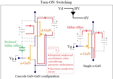
The first advantages is the reduced Miller-effect. As described in Fig. 2, the circuit analysis of a cascode GaN-GaN configuration and a single e-GaN device shows a higher Miller-effect in a single e-GaN during the turn-on switching [5]. The reduced Miller-effect in the cascode GaN-GaN improves the driving capabilities at high-voltage owing to the lower driver requirement to charge the input capacitance.
Fig. 2: Charge and discharge of intrinsic capacitances
in a cascode GaN-GaN and in a single e-GaN during turn-on switching. Adapted from [3].
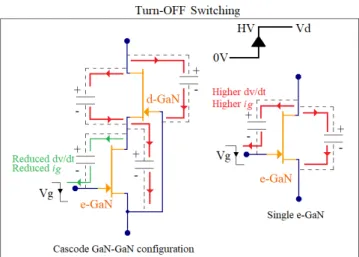
During the turn-off transition, Fig. 3 shows that the configuration GaN-GaN is less affected by a strong dv/dt given the voltage distribution between capacitances. This distribution of voltage represents an advantages in applications of high variations of dv/dt such as in hard-switching power converters. In contrast, the higher flow of current through the parasitic gate inductance in a single e-GaN device during turn-off transitions increases the potential risk of false turn-on.
However, the cascode GaN-GaN configuration has some disadvantages inherent to this type of structures (see Fig. 2). The most critical disadvantage is the influence of the parasitic inductances between the connections of the GaN devices. These parasitic inductances can lead to
Fig. 3: Charge and discharge of intrinsic capacitances
in a cascode GaN-GaN and in a single e-GaN during turn-off switching. Adapted from [3].
undesirable oscillations which are critical in high-frequency operation. Therefore, we address this issue by designing the layout traces in the GaN-GaN configuration with a methodology able to minimize the parasitic inductance.
3
Experimental
test
of
discrete
GaN-GaN configuration
This section describe the experimental setup to asses and compare the performance of a cascode GaN-GaN configuration and a single e-GaN. The experimental setup implements two boost converters with equivalent characteristics as shown in Fig. 4 and Fig. 5. In both cases, the test boards are designed with similar PCB layout, high-frequency driver, and associated passive components. The only difference in both cases is the switching power device. As shown in Fig. 6, the experimental setup records the power converter signals given equivalent test conditions to further comparison.
Fig. 4: High-frequency boost converter using single
e-GaN
Fig. 5: High-frequency boost converter using cascode
GaN-GaN
The two test boards are designed to verify the switching operation of the discrete GaN-GaN configuration and the single e-GaN in a demanding high-frequency boost converter. The circuit for the test consists of a high-frequency boost-converter at 30MHz with characteristics of 200V input voltage, 400V output voltage, and a resistive load of 400Ω - 400W . The test is intended to compare both architectures in a hard-switching and high-frequency application given the demanding switching requirements.
Fig. 6: Experimental setup
In a first low voltage test, the power converters provide 200V to a load of 100W using an input voltage of 100V. In the second case with a higher voltage, the power converters work under conditions of 200V at the input and 400V/400W at the load side. The gate and output voltages are compared in both cases.
Figure 7 shows the gate-source voltage behavior of the e-GaN device for the test at 200V. In this case, the distortion of the gate signal is acceptable in comparison with allowed threshold voltage (Vth). After increasing the voltage and
power requirements, Fig. 8 depicts an important (Vgs) signal distortion. Therefore, the output voltage
signal also trends to be distorted and the risk of power device failure increase. Figure 11 illustrates the distortion of the output voltage in the single
Fig. 7: VGS single e-GaN. Case for low output voltage (200V).
e-GaN configuration when increase the voltage requirement.
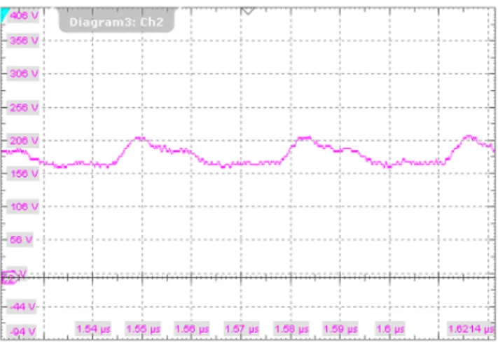
Fig. 8: VGSsingle e-GaN. Case for higher output voltage (400V).
Fig. 9: Output voltage of boost converter at
400V-400W-30MHz. Case single e-GaN
Fig. 10 depict the gate to source voltage (VGnSn)
of the d-GaN device in the cascode GaN-GaN configuration. In this case the output voltage requirement is 200V and the VGnSnkeeps a safety
level. Aditionally, Fig. 11 shows the normal operation of the output voltage at 200V.
Fig. 10: VGnSnfor d-GaN device in cascode GaN-GaN. Case for low output voltage (200V).
Fig. 11: Output voltage of boost converter at
200V-100W-30MHz. Case cascode GaN
In contrast with the single e-GaN configuration, Fig. 12 demonstrates that the gate to source voltage of the d-GaN (VGnSn) keeps a suitable distortion.
Indeed, the d-GaN has a higher Vth level which
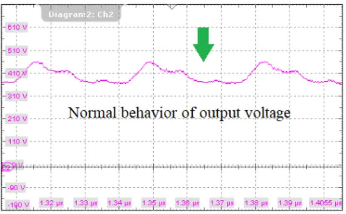
allow a higher distortion level. As a consequence, the output voltage keeps high robustness when increase the voltage and power requirements as shown in Fig. 13.
In comparison with the equivalent e-GaN device, the cascode GaN-GaN configuration shows less sensitivity to the high dv/dt and the VGnSn keeps
safety voltage levels when increase the power conversion requirements. As shown experimentally, the proposed discrete configuration offers a more stable output voltage in demanding hard-switching conditions. The experimental results validate the high-power high-switching capabilities of the
Fig. 12: VGnSnfor d-GaN device in cascode GaN-GaN. Case for higher output voltage (400V).
Fig. 13: Output voltage of boost converter at
400V-400W-30MHz. Case cascode GaN
cascode GaN-GaN configuration. However, the constraints of this higher performance is slightly increasing the implementation complexity and the specific ON-resistance.
4
Conclusion
This paper presented the study and experimental test of a discrete cascode e-GaN d-GaN in a high-frequency boost converter of 400V-400W-30MHz. Experimental results highlighted the stable performance of the GaN-GaN configuration in demanding switching conditions due to the reduced Miller-effect and the lower gate current keeping a more stable gate-source and output voltages. In contrast, the behavior of the single e-GaN under the same testing conditions showed a decreasing performance while increased the voltage and power requirements. As a constrain, the discrete GaN-GaN configuration needed more
implementation complexity and showed higher specific ON-resistance. Further work will provide more details about the selection criteria of the e-GaN d-e-GaN devices and will quantify more power conversion parameters.
Acknowledgements
This work has been partially funded by the Region Occitanie Pyr ´en ´ees-M ´editerran ´ee. The authors would like to thank to Engineer Thierry Sutto of the Exagan company for the helpful suggestions and technical advice through the development of this project.
References
[1] R. Sun, J. Lai, W. Chen, and B. Zhang, “GaN Power Integration for High Frequency and High Efficiency Power Applications: A Review”, IEEE Access, vol. 8, pp. 15 529–15 542, 2020. DOI: 10.1109/ACCESS.2020.2967027.
[2] H. A. et .al, “The 2018 GaN Power Electronics Roadmap”, Journal of Physics D: Applied Physics, vol. 51, 2018.
[3] S. Jiang, K. B. Lee, I. Guiney, P. F. Miaja, Z. H. Zaidi, et al., “All-GaN-Integrated Cascode Heterojunction Field Effect Transistors”, IEEE Transactions on Power Electronics, vol. 32, no. 11, pp. 8743–8750, 2017. DOI: 10.1109/ TPEL.2016.2643499.
[4] M. Murphy, “Cascode Circuit Employing a Depletion-mode, GaN-based FET”, pat. US 7,501,670 B2, 2009.
[5] S. Jiang, K. B. Lee, Z. H. Zaidi, M. J. Uren, M. Kuball, and P. A. Houston, “Field Plate Designs in All-GaN Cascode Heterojunction Field-Effect Transistors”, IEEE Transactions on Electron Devices, vol. 66, no. 4, pp. 1688– 1693, 2019. DOI: 10.1109/TED.2019.2897602. [6] J. Xu, L. Gu, and J. Rivas-Davila, “Low-Loss Gate Driving Techniques of the Cascode GaN/SiC Power Device at High Frequencies”, in 2019 20th Workshop on Control and Modeling for Power Electronics (COMPEL), 2019, pp. 1–6. DOI: 10.1109/COMPEL.2019. 8769703.