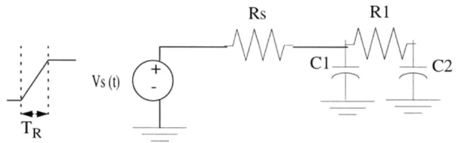
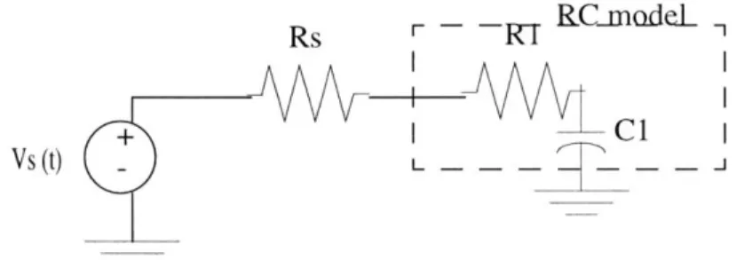
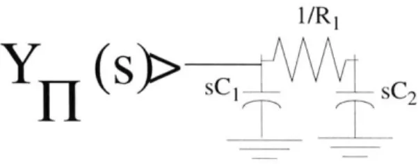
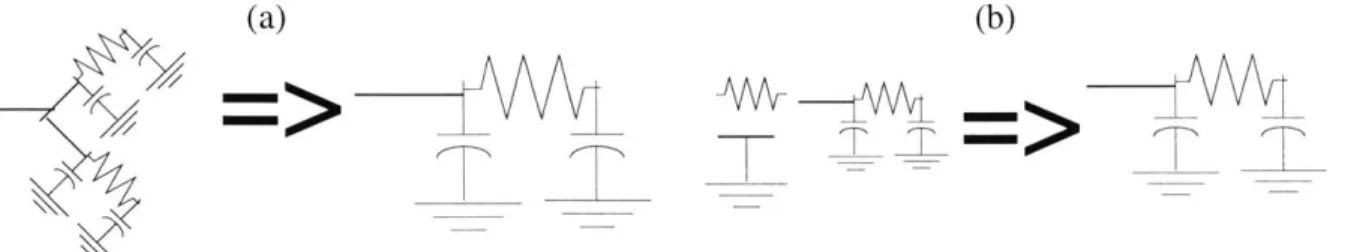
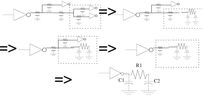
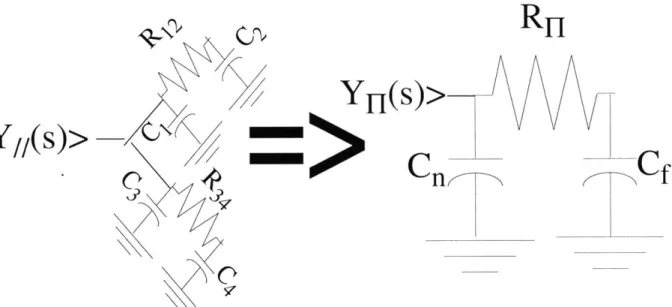
An algorithm to efficiently and accurately compute the effective capacitances of interconnects driven by logic gates
Texte intégral
Figure


Documents relatifs
A reconfigurable point-to-point interconnect (ρ-P2P) is a communication mecha- nism based on DPR that swaps between different precomputed configurations stored in partial
At very short p, of the order of the mean free path, the disorder-averaged intensity propagator does not obey the one-parameter scaling law of the Anderson transition (regime (C)),
From an algorithmic point of view, the main idea of relaxation methods to solve (MPCC) is to compute a sequence of stationary points or more precisely approximate stationary points
This technique, originally introduced in [6; 9; 10] for the proof of disorder relevance for the random pinning model with tail exponent α ≥ 1/2, has also proven to be quite powerful
CJEU case law has, however also held that Member States have a positive obligation to grant and ensure that their courts provide “direct and immediate protection” of rights
Le THC-COOH est détecté 7 à 8 minutes après une prise inhalée. Il est présent en concentration très importante dans le sang. En effet pour une prise de 50 mg de THC inhalée,
In the specific case of the MTD models, the original single- matrix model is parametrized in a bijective way, whereas its gener- alized version with specific transition matrices
the ideal case, the identification of Hollomon law parameter values by instrumented indentation using the model proposed by Ogasawara et al and the cost functional ω
