HAL Id: hal-01727408
https://hal-univ-tln.archives-ouvertes.fr/hal-01727408
Submitted on 9 Mar 2018
HAL is a multi-disciplinary open access archive for the deposit and dissemination of sci-entific research documents, whether they are pub-lished or not. The documents may come from teaching and research institutions in France or abroad, or from public or private research centers.
L’archive ouverte pluridisciplinaire HAL, est destinée au dépôt et à la diffusion de documents scientifiques de niveau recherche, publiés ou non, émanant des établissements d’enseignement et de recherche français ou étrangers, des laboratoires publics ou privés.
Electron microscopy and spectroscopy investigations of
CuOx–CeO2–δ/Si thin films
A. Kopia, K. Kowalski, M. Chmielowska, Christine Leroux
To cite this version:
A. Kopia, K. Kowalski, M. Chmielowska, Christine Leroux. Electron microscopy and spectroscopy investigations of CuOx–CeO2–δ/Si thin films. Surface Science, Elsevier, 2008, 602 (7), pp.1313 - 1321. �10.1016/j.susc.2007.12.041�. �hal-01727408�
Electron microscopy and spectroscopy investigations of CuOz-CeO2-δ/Si thin films
A. Kopia2, K. Kowalski2, M. Chmielowska2,1 ,Ch. Leroux1
1
Université du Sud Toulon-Var, L2MP (UMR-CNRS 6137), BP 20132, 83 957 La Garde Cedex, France
2
University of Science and Technology AGH, Faculty of Metals Engineering and Industrial Computers Science, 30-059 Cracow, al. Mickiewicza 30, Poland
Abstract
CuOx-CeO2-δ/Si thin films were elaborated by pulsed laser deposition. At the surface of all CuOx-CeO2-δ thin
films, Ce4+ and Cu+1ions were present. Depth profiles indicated that a Cu2O rich layer, roughly 40 nm thick,
covered the CuOx- CeO2−δ thin films. Apart from the copper enriched surface, the copper repartition in the thin
films is highly inhomogeneous and two types of copper oxides, CuO and Cu2O, in form of rounded grains 20 nm
were identified in the thin films. At least 10 at. % Cu seems to be inserted in the ceria lattice. Pure CeO2 grains
result from the deposition of tetrahedron-like nanoclusters followed by coalescence of (111) faces, and CuOx
-CeO2-δ grains from the deposition of cube-like nanoclusters followed by coalescence of (110) faces . The good catalytic performances of the CuOx-CeO2-δ/Si thin films are due to active {100} ceria exposed facets covered by
a Cu2O nanoparticles.
Keywords: transmission electron microscopy, X-ray photoelectron spectroscopy, catalysis, thin film structures, cerium, copper, oxides
1. Introduction:
In recent years, mixed oxides catalysts, based on ceria (CeO2) have attracted much
attention. The catalytic activity of oxides is linked to their capability of providing adsorbent oxygen species at their surfaces and to an easy extraction of their lattice oxygen to form
oxygen vacancies [1]. CeO2 is a chemically stable oxide, with an outstanding capacity to store
or release oxygen. This property is linked to the variation of the oxidation state of cerium
between +3 and +4, under various reductive or oxidizing conditions. CeO2 has thus been
widely employed as promoter for precious metal catalysts (Pt, Pd, Au), in the so-called
“three-way catalysts”, (oxidation of CO, oxidation of CnHn, reduction of NO), for automotive
exhaust [1-3]. Stoichiometric CeO2 is known to be an electronic conductor, whereas reduced
CeO2-δ is a mixed ionic/electronic conductor. Thus, doped or substituted ceria films by Fe, Sm, Gd, Zr, Ag, are used in low temperature electrochemical Solid Oxide Fuel Cell, for oxygen storage or transport [4-6], and as active materials in gas sensors [7].
Mixed MOx-CeO2 catalysts were recently envisaged as an alternative to high cost
precious metal components, among them the CuOx-CeO2-δ system was identified as being one
of the most active for CO and CH4 conversion [8-10]. Authors proposed a redox mechanism
for CO oxidation, in which both the support and copper oxides are simultaneously reduced or oxidized. Some works tried to characterize microstructure, oxidation states of copper and cerium, and catalytic properties, for CuOx-CeO2 nanoparticles [11-14]. In most systems,
copper oxide was identified as CuO.
Up to now, thin films of CuOx-CeO2 have aroused much less attention than
nanopowders. Very thin CuO films (8 monolayers) supported on oriented {111} and {001}
CeO2 films were examined by Skärman et al [15]. They showed that copper oxide are more
active for CO gas oxidation on CeO2 {001} than on the CeO2 {111}. This orientation effect
was already evidenced for pure CeO2 thin films [16].
In a previous work [17], we reported our results on the texture evolution of CuOx
-CeO2 thin films with increasing copper content. A change from [111] to [100] in the preferred
orientation of the CeO2 grains was observed. The catalytic properties of the thin films, heated
[18]. The catalytic efficiency was measured by the ratio of the intensity of the CO2 peak to the
intensity of the CH4 peak in IRFT spectra. Nearly no catalytic activity was detected for pure
CeO2 thin films, and the catalytic efficiency increased with the copper content. Full oxidation
of methane was observed for thin films with 27 % at. Cu.
In order to understand these variations in catalytic properties, we studied the
morphology and structure of the CuOx-CeO2-δ thin films by Transmission Electron
Microscopy (TEM) and High resolution Electron Microscopy (HREM). The location of copper was studied by coupling Energy Dispersive Spectroscopy (EDS) analysis, X-ray Photoelectron Spectroscopy (XPS) and Secondary Ion MS (SIMS) measurements. The valences of cerium and copper in the thin films were also determined, by XPS and HREM.
2. Experimental details
2.1 Elaboration of the thin films
Thin films were elaborated by pulsed laser deposition technique (PLD). The targets were
initially prepared by compacting powders of oxide CeO2 and Cu under a pressure of 140 MPa
during 5 min. Then the pellets were sintered at T=1200 ˚C during 2 hours. The final diameter and thickness of each target were respectively of 30 and 3 mm. Pellets with four different nominal copper compositions were prepared, CuyCe1-yO2 with y= 0 – 0.15 – 0.21 and 0.27.
The thin films were deposited on [100] oriented Si substrates (size 1cm x 1cm), using an exciter laser system (Compex 301, λ=248 nm from Lambda Physics, Germany). The characteristics of the deposition system were a fixed laser beam, with a size of 2mm x 5 mm and a target–substrate distance of 60 mm. Oxide thin films obtained by PLD are often non stoichiometric in oxygen and it is well known that working under oxygen pressure can prevent this. Thus, the air pressure in the deposition chamber was P=300 mTorr, a value
¾=45°. Substrates and targets were parallel. The deposition conditions were a fluence µ =1.5
J/cm2, a pulse duration of t =30 ns, and a frequency of f=10 Hz, The substrates were
systematically pre-cleaned in isopropanol, methanol and acetone, before loading in the PLD chamber. During the process, the substrates were heated at 750˚C. A SiO2 layer, 4 nm thick,
subsisted at the surface of the Si substrate.
The various thin films obtained by pulsed laser deposition were labelled “ 100y at. %Cu – t s”, t being the deposition time.
2.2. Characterization of the thin films 2.2.1 X-ray Photoelectron Spectroscopy
The chemical composition of the films was studied by XPS. The XPS spectra were recorded using a VSW (Vacuum Systems Workshop Ltd.) instrument, equipped with a concentric hemispherical 1500 mm electron analyzer and a two-plate 18-channel detector (Galileo). This system was operated with an Al Kα (1486.6 eV) anode, an accelerating voltage of 15 kV and an emission current of 20 mA. The electron analyzer was operated in the fixed-analyze transmission (FAT) configuration, at the energy of 22.5 eV. The background pressure during the analyses was lower than 5.10-6Pa. The binding energy shifts due to surface charging were corrected by fixing the carbon 1s XPS peak at 284.6 eV. The layer analyzed by XPS was estimated to be around 7 nm thick. Thus, in order to acquire XPS spectra at different
depths in the thin films, Ar+ ion sputtering, operating at 2 keV, was used. The spectra
presented result from the summation of 10 scans.
2.2.2 Secondary Ion Mass Spectrometry
The mean distribution of copper and cerium ions, along the growth direction as well as parallel to the substrate, was determined by SIMS. The analyzer was equipped with the
double lens liquid gallium ion beam gun (FEI Company) and the quadrupole mass
spectrometer (Balzers). The energy of the Ga+ ions was 25 keV, and the primary ion current
2nA. The sputtered areas were typically 100*100µm2
. After each sputtering, the depth of the crater was measured with a profilometer. Undesirable crater edge effects were minimized by analyzing exclusively the ion coming from the central 40% of the crater area. Charging effects were eliminated by applying a 250 eV electron flood gun.
2.2.3 Transmission electron microscopy
Cross sectional specimens as well as in plane specimens were prepared by a mechanical thinning process, followed by ion milling. The cross sectional samples were prepared in a conventional way: two 2.5*6 mm2 pieces were glued face to face, and put in a brass rod. The composite was sliced into 250 µm thick slabs, which were mechanically thinned to 100 µm, dimpled on one face down to 20 µm. The ion milling was carried out at low angles +4° and – 6°, the tensions used were at the beginning 5 kV, and were progressively decreased. The in
plane specimens, cut in square pieces 2.3*2.3 mm2, were dimpled and ion milled only from
the back (substrate) of the thin film. A final clean up of the specimens was done at high angle (10°) and low tension (2 kV).
Transmission electron microscopy was performed using a Tecnai G2 operating at 200 kV,
with a point to point resolution of 0.25 nm, and with a JEOL 2010 FEG, operating at 200 kV, with a point to point resolution of 0.19 nm. Images and diffraction patterns were collected with a 1K x1K Slow Scan CCD camera, or on negatives. The morphology of the grains was studied, along the growth direction and perpendicular to the growth direction. The exposed facets were determined. HREM images, coupled with EDS analyses, allowed an accurate determination of the copper species and their location in the thin films. We used microprobe and 20 nm nanoprobe for EDS analyses to quantify the copper amount in the thin films.
3. Results
3.1 Spectroscopic investigation
XPS was used in order to determine the oxidation state of Cu and Ce ions in the thin films and to locate copper species at different depth in the thin films.
3.1.1 Oxidation state of copper and cerium.
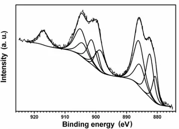
The XPS results for sample 15 at. %Cu-240s are presented Fig.1. The binding energies for copper and cerium are between 870 – 1000 eV (Fig. 1a). Generally, the shape of Ce 3d spectral line in cerium oxides is rather complex due to the overlapping of several component doublet lines (3d5/2 and 3d3/2), resulting from different final states of cerium ion after the emission of photoelectrons [19]. The Ce4+ ions are represented by 3d94f2L-2, 3d94f1L-1 and 3d94f0L configurations while Ce3+ ions are represented by 3d94f2L-1 and 3d94f1L
configurations, where L denotes a ligand. Thus, the presence of Ce4+ ions leads to the
appearance of three doublets in the XPS spectrum and the Ce3+ ions produce two doublet
lines. When these two types of ions are present, five doublets (10 lines) are necessary to fit the Ce 3d region. Only one line situated at 916.7 eV is well separated from the others and corresponds to Ce 3d3/2 (3d94f0L) [19, 20]. The relative intensity of this separated line is 14% of the total Ce 3d line intensity for pure CeO2 compound [20]. This line is absent in pure
Ce2O3 compound. Thus, the relative intensity of this line is a reliable signature for the
presence of Ce4+. For the 0 at.%Cu-240s, 15 at.%Cu-240s and 27 at.%Cu-240s samples, the
relative intensity of this peak was 14%, within the experimental error, indicating an oxidation state 4+ for cerium. More than that, despite a poor signal to noise ration, the Ce 3d region was better fitted with only three 3d doublet lines, characteristic for Ce4+ ion (Fig. 1b). After more
than one hour inside the XPS chamber, samples showed a weak reduction of Ce4+ into Ce3+ ,
The Cu 2p binding energy region, for samples 15 at.%Cu-240s and 27 at.%Cu-240s, showed only one 2p doublet line (Fig. 1c). The binding energy for 2p3/2 was about 932.5 eV
and for 2p1/2 about 952.7 eV, which could correspond to Cu2+ or Cu+ species, within
experimental resolution . It is well established that it is the presence or absence of shake up satellites, that allows to distinguish Cu2+ or Cu+ species [22]. No satellites are observed in the XPS spectra (Fig. 1c), which suggest an oxidation state +1 for copper (Fig.1c). However, due to the poor signal to noise ration, one cannot exclude the possibility of a small amount Cu2+ species.
3.1.2 Distribution of copper species
Two CuOx-CeO2 thin films (15 at.%Cu-240s, 27 at.%Cu-240s) were argon sputtered and
subsequent XPS analyses were done at different depths from the surface. The argon ion etching caused strong reduction of Ce4+ to Ce3+, which is a well known effect [20]. Five 3d doublet lines were necessary to fit correctly the Ce 3d binding energy region (Fig. 2). After several minutes of sputtering the relative intensity of the Ce 3d3/2 separated peak at about 916.7 eV dropped up to 7 % for undoped sample and up to 5-6% for copper-doped samples. The Cu 2p spectra after sputtering showed one 2p doublet line without any shake-up satellites as for previous analyses. Only a small shift of about 0.8 eV toward higher binding energy of the doublet was observed for all samples.
In order to determine the copper content in the thin films, the ratios of the Cu 2p doublet line intensity to the total intensity of Ce 3d lines, for all samples, after each argon etching, were recalculated using the atomic sensitive factors (ASF). These factors are linked to the photo-ionization process and experimental conditions [23, 24]. In this study the factors ASF were equal to 27.1 for Cu 2p and 51.1 for Ce 3d. The obtained atomic ratios of [Cu]:[Ce], and the corresponding at% Cu, are presented Table 1. The results clearly indicate that the surface of
the CuOx-CeO2 thin films is enriched in copper. The copper-enriched surface layer was
estimated to be about 30-50 nm thick.
Using secondary ion Mass Spectroscopy, elemental maps showed that, at a resolution of 1 µm, cerium and copper are uniformly distributed at the surface of the thin films.The in-depth distribution of copper and cerium was also explored. The obtained SIMS in-depth profile for sample 15 at% Cu - 240 s is presented Fig. 3. The detected intensity of 140Ce and 63Cu
isotopes after each sputtering is reported. One can see a higher concentration of copper near the surface. The copper enriched layer is about 40 nm thick. Apart from this layer, the copper content remains constant, though weak, inside the thin films.
3.2 Electron microscopy investigations 3.2.1 Copper oxides
Electron diffraction patterns on cross view samples with high nominal copper content (21 at.% and 27 at. %) and long deposition times (t=240 s and 360 s) showed mainly rings due to the f.c.c. structure of CeO2, with many {111} spots and few {200} spots (see Fig.4). The
two main g200 spots are nearly perpendicular to the substrate. Remember the geometry of electron diffraction, where diffracted beams are due to planes parallel to the incident electron beams, this means that the {200} planes are lying nearly parallel to the substrate. This texture was already observed by X-rays diffraction for CuOx-CeO2-δ/Si thin films [17].In Fig.4, one
can also observe a few extra spots, marked by arrows. The corresponding reticular distances were precisely determined, using the (220) ring of CeO2 for the calibration of the diffraction
patterns, and compared to the reticular distances of metallic copper, cupric CuO, and cuprous
Cu2O oxides. The extra spots were unambiguously indexed either in CuO or Cu2O. The
calculated distances are d1=0.208 nm = d200 Cu2O, d2=0.226 nm = d200 or d111 CuO, d3=0.239
correspond to the ones with the highest structure factor. The same extra spots were also observed in high copper content plane view samples. For lower nominal copper contents, no extra spots were observed.
Individual grains of both types of copper oxides, around 20 nm in size, were imaged and identified by HREM (see Fig. 5 and Fig. 6) in plane view and cross sectional samples.
HREM images of CeO2 grains were used for an accurate calibration of Fast Fourier
Transform (FFT). One can notice that Cu2O grains have a much lower contrast than CeO2
grains in electron microscopy images, and this complicates the identification of copper oxides grains.
3.2.2 Copper oxides location
EDS analyses made on cross sectional samples, by moving systematically the beam parallel to the substrate, near the substrate –thin film interface, showed that the copper repartition in very inhomogeneous in the thin films; for example, in the sample 27 at.% Cu-360s, EDS analyses made with 20 nm nanoprobe size indicated fluctuations from 12 at.% to 30 at.%. Along the growth direction, the Cu content also varied, with a strong decrease of copper content from the substrate-thin film interface to the top of the thin film; for example, in the sample 27 at% Cu-90s, the copper content varied from 30 at% near the interface to 9 at% 100 nm away from the interface. Fluctuations in the copper repartition were also observed in plane view samples. Then, for other cross view samples, or plane view samples, with high nominal copper contents, low copper contents were measured ,around 5-10 at. %, and nearly no fluctuation of the copper content over µm size regions were observed. EDS analyses realized on the 27 at.% Cu-360s thin film, in cross section and plan view samples,
gave around 14% Cu. Finally, nanoprobe EDS analysis on individual CeO2 grains revealed
repartition, and a copper content significantly lower than the nominal copper content of the target.
3.2. Microstructure of the thin films
Generally, the thickness of the thin films deposited by PLD is not homogeneous, thus care was taken to prepare cross sectional samples always from the central part of the 1cm*1cm thin film, in order to be able to compare the different measurements. The thickness of the thin films varied from 200nm to 400 nm, and no link between copper content and film thickness could be evidenced.
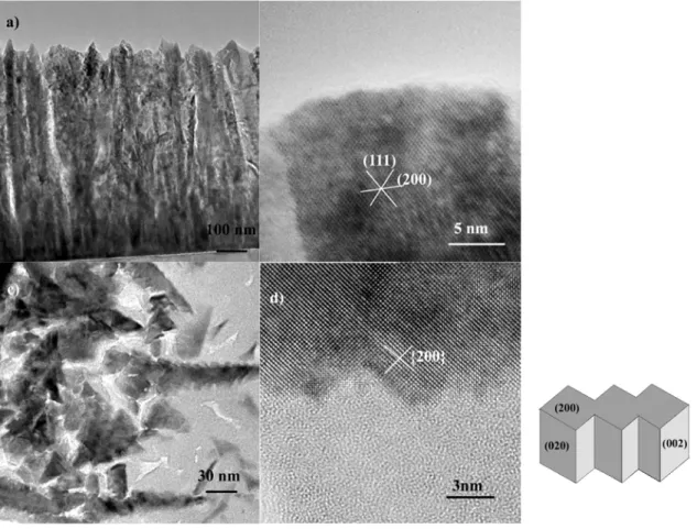
Strong changes in the surface morphology of the thin films with the nominal copper content, were previously observed [17], and related to the texture of the thin films. SEM images revealed triangular features for low copper concentrations, and a [111] film texture, as for high copper content, elongated shapes were observed and linked to the [100] texture. In order to know more about the exposed facets in the thin films, we investigated the microstructure of the cerium oxides grains, both in cross sectional and in plane specimens, for various copper content and deposition times.
For pure CeO2 thin films, the grains have a columnar structure, with some small grains
near the interface, and bigger grains grown from the substrate to the top of the thin film (Fig. 7a). The shapes are rather irregular, but common features can be found, in particular sharp tips and a tendency to broadening away from the substrate. The grains have a mean width of
30-40 nm. HREM images (Fig. 7b) show strong faceting of the CeO2 grains tips, with {111}
planes. The strong faceting appears also in plane view images (Fig. 7c), where one can see a terrace like morphology, with a piling up of flat triangular elements. The grains grow not straight perpendicular to the substrate but are somewhat bent. This is also evidenced in plane views where one observe many [110] oriented grains instead of the expected [111] texture
(Fig. 7d). A schematic drawing of the tip of the CeO2 grains can be proposed, built on
truncated tetrahedral crystals (Fig. 7e).
For copper containing thin films, the growth is still columnar, with grains growing from the substrate to the surface, and some much smaller grains near the substrate. Contrary to pure CeO2 thin films, much of the grain tips are flat (Fig. 8a). HREM images of these tips
indicated (200) planes parallel to substrate (Fig. 8b). The lateral grains size does not differ
significantly from pure CeO2 grains, but the faceting is quite different. TEM plane views
showed that apart for some triangular shaped grains, as in pure CeO2 films, the CeO2 grains
exhibit “Christmas tree” like morphologies (Fig.8c). The facets are now {200} planes, as can be seen in Fig. 8d. A schematic drawing of the shape of CeO2 grains, in copper rich thin films,
is proposed Fig.8e. Thus, the [100] textured grains have exposed (200) facets parallel to the film surfaces, but also many (020) and (002) facets perpendicular to the film surface.
Finally, some small grains near the substrate in cross view samples 15% at. Cu-360s and 27 % at. Cu-360s, were identified as oxygen deficiency cerium oxides; FFT of HREM images could be indexed in Ce6O11, Ce7O12, or even Ce2O3.
4. Discussion
Two copper oxides were identified in the various CuOx-CeO2-δ/Si thin films, by
electron diffraction and HREM imaging, namely CuO and Cu2O. The grains of copper oxides
have lateral sizes around 20 nm. Spectroscopic investigations near the surface of the thin films proved the existence of a 40 nm thick copper rich layer at the surface, with only Cu+. More deeply in the films, the mean copper content was weak, around 8% at. Let us remember that
this mean value accounts for a 104µm2 area. More local EDS analyses, performed on 20 nm
size regions, showed that the copper repartition is highly inhomogeneous. In order to correlate electron microscopy and XPS analyses concerning the copper location, one has to take into
account the thinning process of samples for electron microscopy observations, and a possible preferential milling of copper oxides during the milling process. Copper rich zones on top of
the CeO2 grains were finally observed by electron microscopy, coupled with EDS analyses,
looking at the thickest part of cross section samples, where the top of the films is embedded in the glue, and not thinned by the ion milling preparation process. Unfortunately, because of the thickness and the glue, it was not possible to image this layer by TEM.
Microscopy as well as spectroscopy investigations showed that the mean concentration of copper is low inside the thin films (8-10 % at.), even for high nominal copper content thin films. Nanoprobe analyses realized on individual grains with the f.c.c CeO2 structure showed
a low copper content; this can be interpreted has a substitution of copper into the ceria lattice. Although the insertion of copper in ceria lattice is still controversial [25], existence of solid solution has been proposed by Xiaoyuan et al [26], on the basis of Rietveld refinement of X ray diffraction diagrams. They showed that Ce4+ can be substitute by Cu2+ up to 10 % at. Thus, it seems that the f.c.c. ceria grains in the investigated thin films correspond to a solid solution of roughly 10 at% Cu.
The copper rich layer was identified as Cu2O, but more deeply inside the thin films,
both CuO and Cu2O were observed. Two oxidation states for copper, Cu(I) and Cu(II), were
also observed in nanoparticles CuOx/CeO2 composite catalysts, produced by inert gas
condensation [11]. The fact that the major part of copper is present as Cu2O can be explained
by the use of a metallic copper target, high substrate temperature, and low oxygen pressure in the deposition chamber. Indeed, starting from a CuO target, by varying the substrate temperature and the oxygen partial pressure, Ogale et al. [27] were able to growth Cu2O or
CuO films by PLD. More than that, Itoh et al [28] showed that high temperature substrate favours the growth of Cu2O whereas CuO is obtain for lower substrate temperature, in case of
The peculiar morphology of the CeO2 grains, which can de described as a piling up of
truncated tetrahedron 30-40 nm in size for pure CeO2 grains, suggests a nano-clusters
deposition mechanism. Nanoclusters can be formed in the laser induced plasma plume [29, 30]. The deposition rate of the CuOx-CeO2−δ thin films is around 1 nm/s, which is considered
as a very high deposition rate for pulsed laser deposition [31]. This high deposition rate, along with a high substrate temperature, ensured the coalescence of the nanoclusters, hence the
growth of big CeO2 grains, starting from the substrate. The same nanoclusters formation,
followed by coalescence occurs in CuOx-CeO2-δ thin films, but due to the presence of copper,
the shape of the nanoclusters is not the same. In that case, nanocubes are deposited instead of nanotetrahedron. Thus, the substitution of Ce4+ by copper clearly modifies the kinetic of the different facets. According to Smereka et al [32], depending on the main growth direction and on the relative velocity of {111} and {100} faces, the grains tips in polycrystalline thin films
expose different facets. The relative velocity is characterized by
111 001 3 V V = α . Smereka et al
[32] showed that a [111] growth direction and α =1.1 lead to a surface thin film composed of flat triangular {111} facets, which is the observed morphology for pure CeO2 thin films (see
Fig.7). A growth direction of [001] and α =2.9, lead to square {001} facets (see Fig. 8). Thus, on can conclude that the copper presence greatly increases the velocity of ceria {100} faces with regards to the {111} faces.
Concerning the oxidation state of cerium in the CuOx-CeO2-δ thin films, the
substitution of 10 % Cu2+ in the ceria lattice corresponds to δ=0,1, thus a oxygen deficient ceria. At the surface of the thin films the oxidation state of cerium is 4+, but spectroscopic investigations were unable to distinguish between reduction of cerium due to argon sputtering and intrinsic 3+ state of cerium in the thin films. Small grains of reduced cerium oxides,
Ce6O11 and Ce7O12, were found near the substrate films. The existence of reduced cerium
oxides near the substrate was already observed in pure CeO2 thin films obtained by pulsed
laser deposition [33]. All these results indicate oxygen vacancies in the structure of the thin films.
The good catalytic properties of the CuOx-CeO2-δ thin films can be related to the Cu2O
nanoparticles that cover the 10% at Cu substituted CeO2 grains, combined with the {100}
ceria exposed facets. Skärman et al [15] already observed a better activity for CO oxidation of copper oxide deposited on {100} CeO2 than on {111} CeO2. Recent calculations using first
principles density functional theory showed that {100} surfaces have a lower oxygen vacancy formation energy than {111} surfaces, thus favoured the redox cycle of cerium [34]. Catalytic systems based on Cu2O are rare, and most CuOx-CeO2 systems contain CuO. The catalytic
efficiency of Cu2O thin films was found to be better than the CuO ones by Jernigan et al. [35],
but contradictory results were found by Nagase et al. on nanopowders [36].
5. Conclusion
The CuOx-CeO2-δ /Si thin films obtained by pulsed laser deposition consist of 10 at% Cu
substituted CeO2 columnar grains, covered by a 40 nm thick Cu2O layer. Apart from this
surface layer, nanograins of Cu2O and CuO are present between the CeO2 grains. The thin
films result from the deposition and coalescence of nanoclusters formed into the plasma
plume. The final morphology of the copper substituted CeO2 grains can be explained by the
enhancement of the {100} faces velocity in the presence of copper. The good catalytic properties of CuOx-CeO2-δ /Si thin films is attributed to the Cu2O layer, coupled with the
[100] textured CeO2 grains.
The authors want to thank Ph. Vennéguès (CRHEA-CNRS) for the use of the JEOL 2010 FEG microscope
Figures and tables
Table 1 Atomic ratio [Cu]:[Ce], and corresponding at.% Cu, determined by XPS, after subsequent argon ion etchings.
15% Cu-240s 27% Cu-240s
[Cu]:[Ce] %at. Cu [Cu]:[Ce] %at. Cu
before sputtering 0.41 29 before sputtering 0.46 31,5
20 min sputtering, 0.10 9 20 min sputtering 0.12 11
45 min sputtering 0.08 7,5 45 min sputtering 0.09 8
Fig. 1 XPS spectra obtained for sample 15 at.%Cu-240s after 10 scans (10 min) a) binding energy region for 2p Cu and 3d Ce, b) three 3d doublet lines for Ce4+ ion, c) one 2p doublet line for Cu1+ ion.
Fig. 2 XPS spectra for sample 15 at.%Cu-240s, showing five 3d doublet lines for Ce4+ and Ce3+ ions, after argon sputtering.
Fig. 3 SIMS depth-profile concentration of 140Ce and 63Cu isotopes, showing the location of
copper near the surface of the thin film (realised on sample 15 at. %Cu-360s).
Fig.4 Electron diffraction pattern obtained on a cross section sample
27 at. % Cu-90s . Apart from the ring pattern due to CeO2 grains, supplementary spots
Fig.5 HREM image obtained on a plane view sample 15 at. % Cu-360s, showing CeO2 grains
and one CuO grain. a) FFT corresponding to a CeO2 grain with a [001] zone axis, b) FFT
corresponding to a CuO grain with [011] zone axis.
Fig. 6 HREM image obtained on a plane view sample 27 at. % Cu-90s, a Cu2O grain oriented
Fig.7 Microstructure of pure CeO2 thin films. a) cross section view of sample 0 at. % Cu-240s
b) HREM image of the tip of one CeO2 grain, with a
[ ]
110 zone axis c) plane view of sample0 at. % Cu-240s d) HREM image of one CeO2 grain, with a
[ ]
110 zone axis, e) schematicdrawing of the morphology of one CeO2 grain, resulting from the piling up of truncated
Fig 8 Microstructure of high copper content CeO2 thin films. a) cross section view of sample
27 at. % Cu-360s b) HREM image of the tip of one CeO2 grain, with a
[ ]
011 zone axis,obtained on sample 21 at. % Cu-240s c) plane view of sample 27 at. % Cu-360s d) HREM image of one CeO2 grain, with a
[ ]
100 zone axis, e) schematic drawing of the morphology ofone CeO2 grain, resulting from the piling up of cube like nanoclusters, with the exposed
References:
1. A. Tschöpe, J.Y. Ying, Nanostructured Materials, 4 (1994) 617
2. K.C. Taylor, in Catalysis, Science and Technology, J.R. Anderson, M. Boudart (Eds.), Springer Verlag, Berlin, (1984) 119.
3. A. Trovarelli, Catal. Rev.-Sci. Eng. 38 (1996) 439
4. J.H. Lee, J. Kim, S.W. Kim, H.W. Lee, H.S. Song, Solid State Ionics 166 (2004) 45 5. J.H. Wang, M.L. Liu, M.C. Lin, Solid State Ionics 177 (2006) 939
6. S.Suda, M. Itagaki, E. Node, S. Takahashi, M. Kawano, H. Yoshida, T. Inagaki, Journal of the European Ceramic Society 26 (2006) 593
7. G. Neri, A. Bonavita, G. Rizzo, S. Galvagno, S. Capone, P. Siciliano, Sensors and Actuators B 114 (2006) 687
8. W. Liu, M. Flytzani-Stephanopoulos, Journal of Catalysis 153 (1995) 304
9. A. Tschöpe, J. Y. Ying, Y.M. Chiang, Materials Science and Engineering A, 204 (1995) 267
10. A. Marinez-Arias, M.Fernandez- Garcia, O. Galvez, J.M. Coronado, J.A. Anderson, J.C. Conesa, J. Soria, G. Munuera, Journal of Catalysis 195 (2000) 207
11. B. Skårman,D. Grandjean, R.E. Benfield, A. Hinz, A. Andersson, L. R. Wallenberg,Journal of Catalysis 211 (2002) 119
12. Y. Liu, Q.Fu, M. F. Stephanopoulos, Catalysis Today 93-95 (2004) 241
13. W.J. Zhang , S. PalDey , S. Deevi, Applied Catalysis A: General 295 (2005) 201
14. M.-F. Luo, J.-M. Ma, J.-Q.Lu, Y.-P.Song, Y.-J. Wang, Journal of Catalysis 246 (2007) 52 15. B. Skårman, L.R. Wallenberg, P.-O. Larsson, A. Andersson, ˚J.-O. Bovin, S.N. Jacobsen,
U. Helmersson, Journal of Catalysis 181 (1999) 6
16. M. Lundberg, B. Skårman, L.R. Wallenberg, Microporous and Mesoporous Materials 69
17. M. Klimczak-Chmielowska, R. Chmielowski, A. Kopia, J. Kusinski, S. Villain, Ch. Leroux, J.-R. Gavarri, Thin Solid Films, 458 (2004) 98
18. M. Chmielowska, A. Kopia, Ch. Leroux, S. Saitzek, J. Kusinski, J-R.Gavarri, Solid State Phenomena 99-100 (2004) 235
19. A. Pfau, K. D. Schierbaum, Surface Science 321 (1994) 71 20. X. Yu, G. Li, Journal of Alloys and Compounds 364 (2004) 193
21. E.Paparazzo, G.M.Ingo, N.Zacchetti, Journal of Vacuum Science and Technology A, 9 (1991) 1416
22. H. Zhu, M. Shen, Y. Kong, J. Hong, Y. Hu, T. Liu, L. Dong, Y. Chen, C. Jian, Z. Liu, Journal of Molecular Catalysis A: Chemical 219 (2004) 155
23. J. H. Scofield, Journal of Electron Spectroscopy and Related Phenomena 8 (1976) 129 24. D. Briggs, M.P. Seah, Practical Surface Analysis, 2nd Edition, Vol. 1: Auger and X-ray
Photoelectron Spectroscopy, John Wiley & Sons, 1990, chapter 5.3
25. G. Avgouropoulos, Th. Ioannides, Applied Catalysis A: General 244 (2003) 155
26. J. Xiaoyuan, L. Guanglie, Z. Renxian, M. Jianxin, C. Yu, Z. Xiaoming, Applied Surface Science 173 (2001) 208
27. S.B. Ogale, P.G. Bilurkar, N. Mate, S.M. Kanetkar, N.Parikh, B.Patnaik, Journal of Applied Physics 72 (1992) 3765
28. T. Itoh, K. Maki, Vacuum 81 (2007) 904
29. L.C. Chen in Pulsed Laser Deposition of Thin Films, D.B. Chrisley, G.K. Huber (eds.), Wiley (1994) 195
30. W.Marine, L.Patrone, B.Luk’yanchuk, M.Sentis, Applied Surface Science 154-155 (2000) 345
32. P. Smereka, X. Li, G. Russo, D.J. Srolovitz, Acta Materialia 53 (2005) 1191 33. W.H.Lee, P.Shen, Journal of Solid State Chemistry 166 (2002) 197
34. M. Nolan, S.C. Parker, G.W. Watson, Surface Science 595 (2005) 223 35. G.C. Jernigan, G.A.Somorjai, Journal of Catalysis 147 (1994) 567
![Table 1 Atomic ratio [Cu]:[Ce], and corresponding at.% Cu, determined by XPS, after subsequent argon ion etchings](https://thumb-eu.123doks.com/thumbv2/123doknet/13518939.416780/16.892.100.799.428.1002/table-atomic-ratio-corresponding-determined-subsequent-argon-etchings.webp)
![Fig. 6 HREM image obtained on a plane view sample 27 at. % Cu-90s, a Cu 2 O grain oriented with a [ ]021 zone axis (a), .and a CeO 2 grain oriented with a [001] zone axis (b)](https://thumb-eu.123doks.com/thumbv2/123doknet/13518939.416780/18.892.107.465.186.425/hrem-image-obtained-plane-sample-grain-oriented-oriented.webp)