Achieving Sub-10-nm Resolution using Scanning Electron
Beam Lithography
byBryan M. Cord
MASSACHUSETTS INSTITUTE OF TECHNOLOGYAUG 0 7 2009
LIBRARIES
Submitted to the Department of Electrical Engineering and Computer Science in partial fulfillment of the requirements for the degree of
Doctor of Philosophy in Electrical Engineering and Computer Science at the
MASSACHUSETTS INSTITUTE OF TECHNOLOGY June 2009
© Massachusetts Institute of Technology 2009. All rights reserved.
ARCHIVES
A u th o r ... ... Bryan M. Cord Department of Electrical Engineering and Computer Science May, 2009
Certified by ...: ...
Karl K. Berggren Associate Professor of Electrical Engineering and Computer Science Thesis Supervisor
(/ A
Accepted by ... . ... ... ...
Terry P. Orlando Chair, Department Committee on Graduate Students
Abstract
Achieving the highest possible resolution using scanning-electron-beam lithography (SEBL) has become an increasingly urgent problem in recent years, as advances in various nanotechnology applications have driven demand for feature sizes well into the sub-10-nm domain. While SEBL has the highest resolution of nearly any conventional patterning technique available, reliably defining features at these length scales has been a challenge, as well as an interesting scientific problem.
In this work I have investigated, both theoretically and experimentally, many of the factors that limit SEBL resolution and attempted to understand and minimize their influence on the process. This includes resist development, where we have thoroughly characterized the temperature dependence of poly(methylmethacrylate) (PMMA) resist contrast and used the results to create transferable patterns smaller than nearly any published results to date with this resist chemistry. We have also examined the process of electron-beam exposure and attempted to characterize the various factors that affect the way energy is distributed in the resist by the beam, using theoretical arguments, Monte Carlo simulations, and experimental data. We have used the results of these investigations to create some of the smallest structures reported to date, using hydrogen silsesquioxane (HSQ) resist. Finally, we have applied some of the previously-gained knowledge to the design of a unique bilayer process for patterning high-resolution metal structures using evaporation and liftoff, while simultaneously developing a broadly-useful new model for the kinetics of resist development.
Acknowledgements
This thesis never would have happened without the contributions of the following people, all of whom I feel extremely lucky to have had the opportunity to work with:
Professor Karl Berggren, for supervising my thesis work for the last five years and providing me with much-needed direction and motivation.
Professors Caroline A. Ross and Henry I. Smith, for agreeing to serve on my thesis committee and taking the time to read and give me very constructive feedback on this document.
Dr. Joel Yang, for his endless insights on how to make very small things, his ability to work miracles with an electron beam, and for being a great friend and labmate.
Dr. Huigao Duan, for his transmission electron microscopy expertise and willingness to help me out on very short notice.
Dr. Jodie Lutkenhaus, for always being a phone call or email away when I had a question about polymer or resist chemistry.
Dr. Chris Dames, for his help with constructing the resist-development model in chapter 4.
Dr. Jose Aumentado for designing, and then sharing with me, the original process that led to the work in chapter 4.
Professor David C. Joy, for his insights and assistance in programming the Monte Carlo simulation used in chapter 3, as well as providing the original code it was based on.
Jim Daley, for keeping the NanoStructures Lab running as well as it does, and for helping me fix countless processing problems.
Mark Mondol, for keeping MIT's scanning electron beam lithography facility running smoothly against impossible odds, and also for helping me with all kinds of SEBL work over the years.
Tiffany Kuhn, for being an excellent secretary and for putting up with my frequent and varied last-minute emergencies.
All the other students and staff in the Nanostructures Laboratory, who have always been willing to help me out with random fabrication problems or questions.
Last but obviously not least Kathleen, both for not strangling me at any point while I was writing this thing and agreeing to marry me next month.
Table of Contents
1 Introduction ... ... 1.1 Scanning-Electron-Beam Lithography ... 1.1.1 D escription ... ... 1.1.2 Background and History ... ...
1.2 Motivation for This Work ... 5...
1.3 Thesis Overview ... ... 8
2 Optimizing PMMA Contrast via Control of Development Temperature ...9
2.1 Resist Contrast ... ... 9 2.1.1 Contrast Enhancement ... 12 2.2 Cold Development ... 17 2.2.1 H istory ... ... 18 2.2.2 M echanism ... 18 2.3 Contrast Experiments... ... 22 2.3.1 D escription ... ... ... ... 23 2.3.2 R esults... 28 2.3.3 D iscussion ... 34 2.3.3.1 Scission ... ... 34 2.3.3.2 Crosslinking ... ... 38 2.4 Resolution Experiments ... 41 2.4.1 Description... ... 41 2.4.2 R esults... 43
2 .5 C onclusion ... . ... ... ... ... ... ... 45
3 Control and Optimization of SEBL Exposure ... ... 47
3.1 M otivation ... ... ... ... ... 47
3.1.1 Effect of Exposure Parameters on Resolution ... 47
3.1.2 Limits of Contrast Enhancement ... 50
3.2 The Point-Spread Function ... 52
3.2.1 Primary Beam Scattering ... ... 52
3.2.2 Beam Diameter and Secondary Electrons...56
3.3 M onte Carlo Sim ulation... ... ... 59
3.3.1 D escription... ... 59
3 .3 .2 R esu lts ... ... ... 6 3 3.4 Experimental Verification...70
3.4.1 Description...70
3.4 .2 R esults ... ... ... .. ... ... 72
3.5 Beam Diameter Measurement...77
3.5.1 Procedure ... 77 3.5.2 R esults ... ... ... 79 3.6 Imaging Limitations... 81 3.6.1 TEM Analysis ... 83 3.6.1.1 Sample Preparation ... .... 83 3.6.1.2 R esults ... .... ... 86 3.7 HSQ Development ... 88 3.7.1 Development Rate... 88
3.7.2 Diffusion-Limited Development... ... 90
3.7.3 Experimental Verification...94
3.8 Conclusion and Further Work...97
4 High-Resolution Liftoff Patterning with a Lithographically-Defined Bilayer ....101
4.1 Electron-Beam Evaporation... 101
4.2 Suspended Shadow-Mask Evaporation... ... 103
4.2.1 Process O verview ... 103
4.2.2 Bilayer Fabrication... 105
4.2.2.1 O verview ... 1... 05
4.2.2.2 Copolymer Method ... 105
4.2.2.3 Poly(methylglutarimide) (PMGI) Method... 108
4.2.3 Lithographic Undercut Control... 109
4.3 Exposure Modeling ... 113 4.3.1 D escription... 113 4.3.2 Results ... ... ... ... 115 4.4 Experimental Verification... 117 4.4.1 Procedure ... ... 117 4.4.2 R esults... 117 4.4.3 U ndercut Saturation ... 119 4.5 Development Modeling ... 120 4.5.1 Model Description ... ... 121
4.5.2 Derivation of Undercut Relationship ... 123
4.6 Applications and Conclusion ... 129
5 C on clu sion ... ... ... ... 134
5.1 Resist Processing Limitations ... 134
5.1.1 PM M A ... 135 5.1.2 H SQ ... .136 5.2 Metrology Limitations ... 138 5.3 Summary ... 138 5.4 Further W ork... 140 Appendix A A.1 A.2 Monte Carlo Source Code... ... 141
Interface ... 14 1 Source C ode ... 145
A.2.1 Global Variable Declaration ... 1...146
A.2.2 The XYZ Data Type ... ... 148
A.2.3 Main Program Loop ... 149
A.2.4 Secondary Electron Tracking...158
Chapter 1: Introduction and Overview
Since its inception, the semiconductor industry has been marked by a constant demand for better, more high-resolution ways of patterning devices. Moore's Law, which states that the number of transistors that can be practically placed on an integrated circuit will double every two years,1 has driven decades of relentless improvement of lithographic technologies. As resolution demands begin to approach the scale of atoms and molecules, long-dominant technologies such as optical projection lithography are proving increasingly difficult to improve further. Scanning-electron-beam lithography (SEBL), a low-throughput technology capable of much higher resolution than any current photon-based scheme, may hold the key to enabling the next generation of mainstream lithographic technologies. In this work, we seek to understand the capabilities and limits of modern SEBL processing, from both a theoretical, scientific point of view and in the
context of several different applications.
1.1 Scanning Electron Beam Lithography
Scanning-electron-beam lithography has existed nearly as long as the semiconductor industry itself. Its extremely high resolution (the highest of any practical lithographic technology) has made it invaluable for photomask manufacture, research work, and other applications, but its inherently low throughput has kept it from replacing lower-resolution optical projection lithography in large-scale manufacturing settings. Still, SEBL may represent the key bridge between current and next-generation lithographic technologies.
1.1.1 Description
Scanning-electron-beam lithography is a process that, since its invention nearly four decades ago,2-10 remains one of the highest-resolution methods of top-down nanopatterning available. Steady improvement of SEBL tools and processes over the years has led to current state-of-the-art systems capable of producing structures on the order of 10 nm widel'- 16-more
than a factor of four better than even the most cutting-edge photon-based lithography. While throughput limitations have kept SEBL from being used in high-volume manufacturing by the semiconductor industry, it remains a key technology for mask-making, research, application-specific integrated circuit (ASIC) manufacture, and other applications where resolution is critical and throughput is not a major issue.
1.1.2 Background and History
SEBL is a relatively self-explanatory technology--a tightly focused beam of electrons is scanned across a sample coated with some type of electron-sensitive material. By switching the beam on and off and controlling its speed and direction, patterns can be formed in the material. The technology has its roots in scanning electron microscopy (SEM), and was inspired by the fact that a SEM 1) is capable of much higher resolution than any optical microscope, and 2) can damage certain types of samples under inspection if the beam is focused on them for too long. The first SEBL systems were
simply electron microscopes, reprogrammed to generate simple shapes, like lines, instead of the standard raster-scan display used for imaging.78'
The results of these early SEBL experiments were extremely promising, and dedicated SEBL systems with hardware-based beam controllers eventually took the place of the software-controlled, "hacked SEM" systems used in the earliest experiments, as shown in figure 1-1.17-19 At the same time, considerable effort was being expended toward discovering high-resolution electron resists to complement the new technology.
3'-59' 10 ,20-23 While many types of resist were investigated, poly(methylmethacrylate) (PMMA), quickly became (and remains today) the most commonly-used due to its high resolution, chemical stability, and versatility.2 4
-2 6 Being the dominant resist, PMMA was extensively characterized, and its exposure and development mechanisms remain among the most well-understood of any high-resolution resist currently available.
'fomputer
Cii
,d4 ...
Qici9 r ; J
L In terface
Figure 1-1: The evolution of scanning electron beam lithography tools. Left: Block diagram of
an early custom-built SEBL system used by Herzog et al in their 1971 paper.7 Right.: The Vistec
VB300, a modern, production-grade dedicated SEBL tool. (Photo courtesy Vistec, Inc.)
As the scanning electron microscopy state of the art improved through the years, SEBL improved along with it. Better tools, with more tightly-focused beams, faster and more accurate pattern generators, and higher acceleration voltages became available, and the resolution of the technology improved accordingly. At the same time, theoretical and experimental work was being done to try to fully understand the fundamentals of electron-resist interaction4-6'21
,23,28,30,34-41 and, in the process, determine whether this
progress would continue indefinitely or if some ultimate factor would set a final resolution limit for SEBL.32'42'43
1.2
Motivation for This Work
Modem, state-of-the-art SEBL systems are capable of fabricating structures on the order of 10 nanometers wide. While this length scale is extremely small and far beyond what any practical top-down lithographic process can achieve, recent applications demand even better patterning capability.
Nanoimprint lithography, schematically diagrammed in figure 1-2, is a promising next-generation technology for large-scale semiconductor fabrication, as patterning structures smaller than about 25 nm using conventional optical projection lithography (OPL) has proven increasingly difficult. The logical technology to fabricate the imprint masters is SEBL-by quickly replicating a single SEBL-fabricated master mold many times, imprint lithography retains the key strength (high resolution) of SEBL while avoiding the throughput issues that are its key weakness in large-scale production applications.
While the semiconductor industry has been using SEBL-generated photomasks for optical projection lithography in much the same way for decades, the analogy between optical projection and nanoimprint lithography is imperfect for several reasons. Unlike conventional optical projection lithography systems, which typically use a lens to reduce the pattern on the photomask by -4x before printing the final pattern, nanoimprint lithography requires the features on the master mold to be the same size as the features on the final pattern. This means that the success of nanoimprint lithography is directly tied to the resolution capabilities of electron-beam lithography-if nanoimprint is going to be
proven to be demonstrably better than optical projection lithography, it requires SEBL technology capable of manufacturing master patterns with critical dimensions of 10 nm and smaller.
wn
0 0
Figure 1-2: Schematic illustration of nanoimprint lithography. A master mold is stamped into some type of soft material, transferring the pattern on the mold into the material. For obvious reasons, the image-reduction methods that simplify mask-making in optical projection lithography are inapplicable here..
A less immediately practical, though potentially more far-reaching, application of high-resolution SEBL is templated self-assembly. As nanotechological applications call for complex structures with smaller and smaller critical dimensions, it makes increasing sense to fabricate structures "from the bottom up"-that is, by co-opting natural self-organization and self-assembly processes to assemble structures from their component parts-rather than with "top down" technologies such as lithography. Templated self-assembly-the process of using physical and/or chemical "templates" to force very small structures into useful, orderly patterns-is a fundamental first step in this direction. Our group and others have had some recent success, some results of which are shown in
figure 1-3, in templating block copolymers (BCPs)44-48 and sub-10-nm semiconducting
quantum dots, to name just two examples.
Figure 1-3: Left: 8-nm-wide CdSe quantum dots forced into a hexagonal lattice by
10-nm-wide Ti-Au lines fabricated using SEBL. Right: Block copolymers organized into a
lattice using 12-nm-wide hydrogen silsesquioxane (HSQ) posts (bright points) as guide
structures (micrograph courtesy J Yang).
The question of SEBL resolution arises in templated self-assembly because SEBL, by enabling fabrication of the templates, provides the "bridge" between top-down and bottom-up fabrication. Since the top-down process has to be able to pattern template structures on the order of the size of the materials being templated, the resolution of the top-down process is currently a limiting factor in templated self-assembly. With groups successfully manufacturing quantum dots that are only 2 nm in diameter,49 there is virtually unlimited demand for better SEBL resolution in this area.
From a purely scientific standpoint, understanding the resolution limit of SEBL, and the factors behind it, is extremely interesting. Quite a bit of work has been done over the years in this regard,3 2,42,43 but the predicted resolution limits have been repeatedly broken.
As tool technology improves and better resist-processing methods are developed, more and more non-fundamental resolution barriers are removed, allowing an unprecedented opportunity to investigate the technology's possible true, fundamental resolution limit.
1.3
Thesis Overview
The thesis will begin with discussion of a technique for optimizing PMMA contrast by controlling development temperature, providing an overview of the many contrast-enhancement techniques developed over the years in the process.12 Chapter 3 will
present a thorough theoretical and experimental study of electron-solid interactions and attempt to describe the current limits of SEBL resolution and the mechanism behind it. Chapter 4 will discuss a novel process for high-resolution metal evaporation and liftoff developed in the process of fabricating high-resolution Josephson junctions.50 This
chapter will also discuss some of the concepts introduced in the previous two chapters in a more applications-based context.
Chapter 2: Optimizing PMMA Contrast via Control of
Development Temperature
Many of the previously-discussed applications of nanolithography, such as templated self-assembly and nanoimprint master templates, require feature diameters on the order of or smaller than 10 nanometers. While patterning structures as small as 15 nm with SEBL is relatively trivial, getting beyond this resolution can be problematic, as factors like beam diameter, electron scattering, and resist contrast can no longer be ignored. In this section, we discuss the results of an attempt to increase the contrast of PMMA using a temperature-optimized development process, and as a result push our final process resolution into the 10-nm regime.
2.1
Resist Contrast
Resist contrast is a relatively simple metric for determining how "good" a resist is. Contrast measurements are typically performed by exposing several features on a resist-coated sample at different doses, developing for a fixed time, then measuring the amount of resist remaining post-development as a function of dose. The final "contrast curve" is usually plotted as remaining resist thickness (normalized to the initial thickness) vs. dose, although dissolution rate as a function of dose is also used and is more useful as it makes the measurement time-independent.
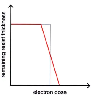
As figure 2-1 shows, an ideal contrast curve looks like a step function; below the threshold dose, no resist development takes place, while above the threshold dose the development rate is effectively infinite. This behavior, unfortunately, cannot be achieved with real-world materials, and experimentally-measured contrast curves generally look similar to the red curve in 2-1, with a sloped region between the dose at which the resist starts to develop (Do) and the dose at which the resist fully develops away (DI). Contrast is generally quantified with the following expression:
7Y= log J (2.1)
Where y is defined as the contrast, essentially the slope of the region between the Do and D1 doses. The higher the y the better the resist contrast; a resist process with perfect
.c
E
electron dose
Figure 2-1: Schematic illustration of infinite (black line) and finite (red line) contrast, plotted as remaining resist thickness as a function of electron dose. In the infinite case,
the transition from no development to full development happens at a single critical dose, while in the more realistic finite case the transition occurs more gradually.
It is important to mention that resist contrast is an extremely non-fundamental measurement. Resist thickness, developer type, development time and temperature, and any number of other external parameters are convolved into contrast measurements along with resist "quality." As a result, using resist contrast to make blanket statements about the fundamental capabilities of a resist (e.g. "PMMA is a better resist than HSQ because it has a higher contrast") is inappropriate; resist contrast should only be used to directly compare different resist processes, in which all of the previously-mentioned parameters are clearly specified. While this would seem to limit the usefulness of resist contrast as a metric, its ease of measurement and ability to evaluate the effect of a single parameter on
a resist process (as we will see in the following sections) make it an important, if limited, tool for the study of resist behavior.
2.1.1 Contrast Enhancement
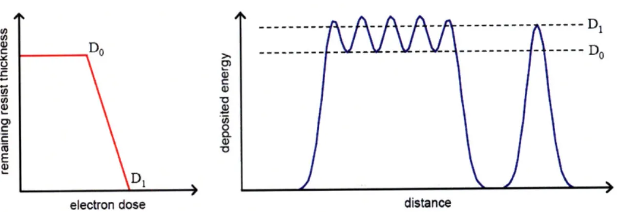
All other things being equal, an increase in contrast translates directly into an increase in process resolution. To illustrate this, consider the idealized dose profile in figure 2-2.
D(x)
D
M4X
AXFigure 2-2:. D dose profile of an idealized sinusoidal grating structure. The doses DMAx
and DMIN define the dose modulation of the grating.
The dose modulation function for the grating structure in figure 2-2 can be defined as:
M
D - MAX - DMIN (2.2The modulation in the dose profile of a grating structure is inversely proportional to its pitch, which will be discussed in more detail in chapter 3.
We now consider two schematic contrast curves, one with high contrast and one with low contrast as defined by eqn. (2.1).
resist
thickness
Ro
dose
Do DIA DB
Figure 2-3: Schematic contrast curves (in remaining resist thickness vs. dose format) for
two hypothetical resist processes, one with high contrast (green curve) and one with low
contrast (red curve). Ro is the initial resist thickness; Do is defined as the minimum dose
at which resist development occurs and D1 is defined as the minimum dose at which the
resist fully develops away after a set development time. The difference between the two
The curve shows how much of the initial resist thickness Ro remains as a function of dose, after a set development time tD. The dose Do is defined as the minimum dose at which any resist development occurs; the dose D1 is the minimum dose at which the
resist fully dissolves away after time tD. We can define a contrast modulation function similar to equation (2.2) using these curves:
D -
D
D,
+ Do
(2.3)
Superimposing the information in figure 2-3 on figure 2-1 begins to suggest the relationship between contrast and resolution.
D(x)
---
D1I WX
Figure 2-4: Dose profile offigure 2-2 with the relevant doses from the contrast curves in
figure 2-3 superimposed. In the part of the pattern where the dose is below Do, no
dissolution of the resist takes place during development. In the high-contrast case, full
development happens when the dose is greater than DIA, with partial development
happening when the dose is between Do and DIA. In the case of DiB, where the contrast
modulation function exceeds the dose modulation function, all of the pattern lies in this
in-between regime and none of the features willfully develop.
In the high-contrast case in figure 2-4, the resist dosed above DIA will fully dissolve away, the resist dosed below Do will not develop at all, and any resist in the region between the two doses will undergo some partial development, which will result in the slightly sloped sidewalls shown in the final developed pattern in figure 2-5(a). In the case of the low-contrast resist process, the contrast modulation function exceeds the dose
modulation function (Mc > MD), which means that none of the resist in the pattern will develop fully away, leading to the resist profile shown in figure 2-5(b). The resist contrast, then, defines the amount of dose modulation required for a pattern to yield. Since dose modulation is inversely proportional to pattern density, higher contrast enables the patterning and successful development of smaller, denser structures.
D(x)
A
D(x)B
--- D, --- --- --- --- --- ---- --- D ...- --- -- --- -- --- D NA Do -N--"---V---\--Do---Figure 2-5: Final developed resist profiles for the dose modulation function shown in figure 2-2 and the contrast curves offigure 2-3. In case A (the high-contrast process) the resist has yielded a recognizable grating structure with only slight inward sloping of the sidewalls, which is unavoidable with any finite-contrast resist. In case B (the low-contrast process), however, none of the resist has fully cleared, creating a final structure
with severely sloped sidewalls and no exposed substrate. Postprocessing on this type of resist profile is generally impossible, so the pattern in case B cannot be said to have yielded.
As our idealized example illustrates, there is at least in principle a strong correlation between resist-process contrast and lithographic resolution. As a result, many different chemical and mechanical methods have been attempted in order to improve the resist contrast in electron beam lithography processes. 3051,52 Of these methods, one of the most successful (at least in the case of PMMA'5 and similar resists, such as ZEP52053) has been cold development-simply developing the resist in a developer solution cooled below room temperature.
2.2
Cold Development
The vast majority of photo- and electron resists in use today are developed in aqueous or organic solvents kept at or near room temperature (25°C). The reason for this is primarily convenience-room-temperature developers do not need bulky and costly temperature-control equipment. Coupled with the fact that development contrast is not a limiting factor in most processes, this has until recently discouraged widespread investigation of the effect of developer temperature on contrast. As electron beam lithographers have struggled to improve process resolution even marginally, though, it was inevitable that development parameters in general, and developer temperature in particular, would eventually be examined in great detail.
2.2.1 History
Cold development of PMMA was pioneered approximately a decade ago; a 1998 paper by Pantenburg et al is one of the earliest references to it in the literature.54 As feature size
was not a major concern (or was limited by factors other than resist contrast) at this time, early papers on cold development focus on its efficacy in improving resist sidewall profiles, resulting in cleaner and more robust pattern transfer.51'54 It was not until 2004
that improving lithographic technology allowed cold development to be examined purely as a resolution-enhancing technology by Hu et al,15 but it appeared to be a qualitative
improvement in this regard as well.
Though cold development was widely adopted by the electron-beam lithography community following publication of the Hu paper, the mechanism behind its contrast enhancement was still poorly understood. This was remedied by a 2006 paper by Ocola et al, which gave a detailed, plausible explanation for the success of cold development.53
2.2.2 Mechanism
PMMA, as is well-known, is a chain-scission resist; that is, it is exposed when incident photons or electrons break bonds in long PMMA molecules and turn them into several shorter molecules. When exposed to organic solvents, the short PMMA chains created by scission are able to dissolve away, while the long, unexposed chains remain entangled in a matrix and stay in place. The relationship between the molecular weight of a PMMA
molecule and its solubility is extremely nonlinear, which makes it an excellent, high-contrast electron beam resist under almost all processing conditions.2 1'2 6
The mechanism by which cold development causes an enhancement in resolution is not widely understood. Ocola et al have suggested that the key lies in the glass transition temperature (Tg) of PMMA.53 This theory assumes two things: that the glass transition temperature (Tg) of a PMMA molecule is proportional to its molecular weight,55 and that PMMA molecules will dissolve away when placed in a solution with a temperature above their glass transition temperature. The theory relies on the fact that, when a feature is exposed in PMMA using an electron beam, resist around the edges of the feature is partially exposed due to scattering of the beam, secondary electron generation, and other effects, resulting in medium-length, partially-exposed molecules surrounding the short molecular chains of the exposed area.56 When developed at room temperature, some of these partially-exposed chains will be above their Tg and thus able to develop away, resulting in a biasing of the exposed feature. When the developer is cold, however, its temperature is below the Tg of these molecules; as a result, more of the partially-exposed PMMA is "frozen" in place and the final developed feature matches the dimensions of the exposed one much more precisely. While this theory has an attractive simplicity, it contains several questionable assumptions. The suggestion that PMMA chains with
Tg<Tdeveloper will dissolve during development while chains with Tg>Tdeveloper will not
ignores the fact that the glass transition temperature, when applied to polymers, is not a clear delineation point at which previously stationary material begins to flow. Moreover, Tg is a bulk property and not designed to apply to single molecules; the effect of
polydispersity (the distribution of molecular weights present in both the exposed and unexposed resist) on the process, if any, is not addressed at all.
Another possible explanation of the cold-development mechanism takes some of the unaddressed issues in the Ocola theory into account. When a small feature is exposed in PMMA, the continuous nature of the deposited energy density in the resist will result in boundary region between the "exposed" and "unexposed" sections of the resist, as illustrated in figure 2-6(a). While the exposed region of the resist will consist almost entirely of soluble polymer fragments and the unexposed region of insoluble molecules, this boundary region will contain both soluble and insoluble polymer fragments, due to both the initial polydispersity of the PMMA and the random nature of chain-scission events.57 When placed in developer, the molecular fragments in the boundary region will have a tendency to phase-separate; the soluble fragments will diffuse toward the exposed region and the insoluble fragments will diffuse toward the unexposed region, eventually resulting in a wider region of soluble polymers as shown in figure 2-6. Since phase separation can be described by diffusion, which is a temperature-dependent process,58
developing at low temperatures will inhibit this separation, preserving the boundary region (which will be indistinguishable from unexposed resist when removed from the developer5 9) and resulting in a narrower developed feature.
soluble
soluble/insoluble mixture
i,
insolublefinal linewidth
Figure 2-6: Schematic illustration of one possible explanation of the
resolution-enhancing mechanism of cold development. When a feature is exposed in PMMA, the
soluble resist in the exposed region is surrounded by a boundary region of resist that, due
to the initial polydispersity of the PMMA and random nature of chain scission, contains
both soluble and insoluble polymer chains (1). During development, this region
phase-separates, with the soluble chains diffusing toward the soluble region and the insoluble
chains diffusing toward the insoluble region (2). The result is a region of soluble PMMA
that is larger than the initial exposed feature, resulting in a degradation in resolution (3).
Cold development helps prevent this by limiting the diffusion that can occur in the
A third possibility is that maximum size of a polymer chain that can be removed from the PMMA matrix and dissolved is a temperature-dependent parameter itself. This is a plausible theory as the motion of the solvent molecules in the solution is Brownian and, as a result, temperature-dependent; at higher temperatures, solvent molecules can exert a greater force on PMMA chains and, as a result, dislodge larger polymer molecules from the matrix. In this case, lowering the temperature decreases the maximum molecular weight that can be dissolved which, given the spatial molecular-weight distribution of an exposed feature, will result in increased contrast and resolution.
Regardless of the exact mechanism responsible, cold development indisputably has a beneficial effect on real-world resolution. Knowing this, the question of which "cold" temperature should actually be used becomes relevant. Published data shows a clear trend toward finer resolved features with reduced developer temperature,15 but the lowest
developer temperature reported in the literature is -17 C.5 3 This is substantially higher
than the freezing point of most PMMA developers (probably the ultimate practical lower limit to developer temperature), and suggests that even higher resolutions may be possible by developing at extremely cold temperatures.
2.3 Contrast Experiments
As previously-published cold development work had stressed the relationship between PMMA contrast and development temperature, our initial investigation of
ultra-low-temperature PMMA development focused on measuring the contrast over as wide a range of "cold" temperatures as possible.
2.3.1 Description
Commercially-available PMMA with an average molecular weight of 950K was used in all of our contrast experiments. For simplicity, our standard in-house developer (3:1 isopropanol:methyl-isobutyl-ketone), which has a freezing point of approximately -80'C, was also used in all experiments. By combining several cooling methods, we were able to measure contrast data at temperatures ranging from 15 to -60'C. For the 15 to -30'C
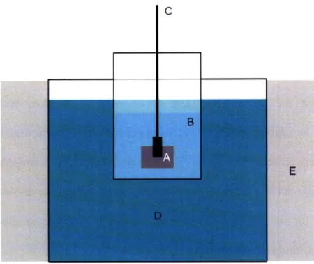
temperature range, we used a commercially-available Ladd Research Stir-Kool thermoelectric chiller in the configuration shown in figure 2-7. This system had the advantage of being equipped with both a temperature controller and a magnetic stirrer, allowing us to control temperatures to within 0.1 C as well as keep the developer stirring continuously to ensure uniform temperature throughout the bath.
Figure 2-7: Schematic diagram of our cold-development system based on the Ladd
Research Stir-Kool thermoelectric chiller. The sample to be developed (A) is immersed
in a beaker of developer (B) via a dipstick with an alligator clip to hold the sample at the end (C). The beaker sits on a thermoelectric block (D), which is regulated using a
thermocouple (E) connected to a temperature-control system inside the Stir-Kool unit
(F). In order to get maximum efficiency from the chiller, the beaker was sheathed in
foam insulator to minimize atmospheric heating of the bath (G). A magnetic stirrer (not
shown) in the bath ensured temperature uniformity by keeping the developer in constant
motion.
The Stir-Kool unit was not powerful enough to cool our developer below about -30°C, so for colder temperatures the dry ice bath system in figure 2-8 was used. The procedure consisted of immersing a beaker containing a large amount of developer in a larger beaker containing a mixture of dry ice and isopropanol, which would typically reach
about -75°C. The temperature of the developer was continuously monitored as the entire system was allowed to slowly warm up to room temperature. The volume of the developer was chosen so that its thermal mass would keep it from warming by more than about 1"C per minute. Temperature uniformity was maintained by manual stirring of the developer with the thermometer, and development at a given temperature was accomplished by simply waiting for the developer to reach that temperature and running the development process; for a 60-second development, this gave a temperature accuracy of +10C. While not as precise as the Stir-Kool-based system, the dry-ice-bath method was adequate for our purposes and produced results that were reasonably repeatable if care was taken during the processing.
Figure 2-8: Schematic diagram of the dry ice bath used to develop PMMA at
temperatures below -30 °C. The sample (A) is immersed in a large beaker of developer
(B) using the same alligator-clip dipstick as figure 2-7 (C). The beaker of developer is
suspended in a bucket of dry ice and isopropanol with an initial temperature of --75C
once the developer has warmed up to the desired development temperature. To slow the
warming process, the bucket was wrapped in thermal insulation (E) to help thermally
isolate it from the environment.
In both cases, the development procedure was identical: the sample would be attached to a dipstick via an end-mounted alligator clip, then immersed in the developer for a given length of time (generally 60 seconds). At this point, standard procedure would be to rinse the sample in isopropanol or some similarly weak solvent to remove the developer, but any room-temperature solvent rinse will significantly degrade the resolution gain from
the cold development, so the samples are simply removed from the bath and dried. The drying step is critical; a 1 cm2 sample must be dried under a N2 gun for 60-90 seconds.
This time is to allow the sample to return to room temperature; if it is exposed to atmosphere while still cold, water vapor will quickly condense on the sample and form a thin sheet of ice on the surface, which will generally distort and crack the PMMA film.
Contrast curves were measured by using out Raith-150 SEBL system to expose a series of large (20 x 100 !lm) bars at a range of doses that increased on a logarithmic scale on a 160-nm-thick PMMA film, then developing the sample at a given temperature for a fixed period of time. The acceleration energy of the beam was 30 keV, and the areal doses varied from 100 pC/cm2 to 3000 pC/cm2 depending on the development temperature. The large size of the features served two purposes: it ensured that diffusion of the developer into the feature had a negligible effect on development rate (see chapter 4) and also made profilometry measurements much easier by ensuring that the features could be easily found in an optical microscope. The height of the resist remaining in each bar was measured using a Tencor P10 profilometer. Since PMMA is a soft material, it was critical to use a low profilometer stylus force to get an accurate reading here. A force of 5 mg seemed to be low enough to not distort the film; measurements taken at this stylus force were nearly identical to measurements taken on the same sample using an atomic force microscope.
2.3.2 Results
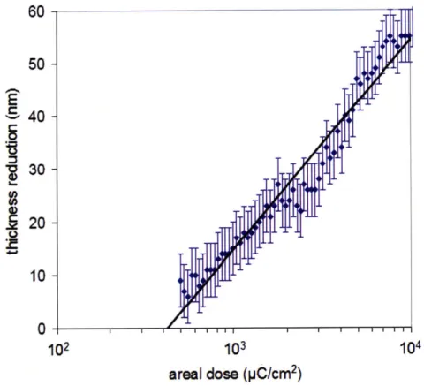
Before discussing the results of the contrast measurements, one interesting effect should be mentioned. After exposing a sample, the extremely-highly-dosed bars were visible immediately after removal from the SEBL tool; in other words, the resist was being altered even before development at high doses. The profilometry measurements in figure 2-9 showed that this was due to resist contraction and followed a logarithmic trend. The mechanism behind this resist contraction during exposure will be discussed in more detail later; for now, it is only relevant because the contraction varies the initial (pre-development) thickness of the resist; when calculating the amount of resist dissolved during development, the measurements in figure 2-9, and not simply the initial resist thickness, must be used as a baseline at high doses.
60 50 -S40 - 30 200 10 0-0 102 103 104 areal dose (pC/cm2)
Figure 2-9: PMMA thickness reduction before development as a function of areal dose,
measured via profilometry during contrast curve experiments. The error bars here were
determined by repeatedly measuring a single feature with the profilometer and
calculating the standard deviation of the measurements. For low doses (<1000 puC/cm2)
this contraction effect is negligible, but at higher doses the resist can contract by 50 nm
or more, which must be taken into account when calculating development rates using
final and initial resist thicknesses.
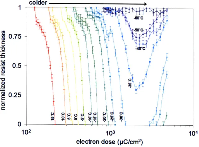
The measured contrast curves for temperatures ranging from 15 to -60'C are shown in figure 2-10:
colder
1-0 T
-
0.75-
c
0.5
0.25 -J
0
102
103
104
electron dose (pC/cmn
2)
Figure 2-10: Measured contrast curves for PMMA developed in 3:1 IPA:MIBK at various temperatures. The initial resist film thickness was 160 nm and the development time was 60 seconds, except in the -40 'C and -50 'C cases (120 seconds) and the -60 'C case (600 seconds), where longer development times were needed to show any measurable dissolution at all. The contrast (in cases where the resist fully cleared) was measured by calculating the slope of a given curve from the 0.75 (75% of initial resist remaining) dose to the dose where full development occurred The error bars in this case represent the inherent uncertainty of the profilometer, the characterization of which is discussed in the caption offigure 2-9.
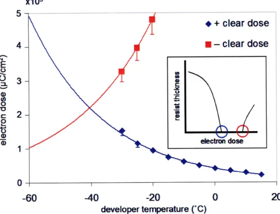
There are two immediately noticeable trends in figure 2-10. The first is the change in sensitivity-as the development temperature is reduced, the clear dose increases almost
exponentially. The second is that, at low temperatures and high doses, a "tone reversal" effect is observed-additional dosing actually causes the resist to develop more slowly, making PMMA effectively behave like a negative resist.6 0
,6 1 The tone-rehearsal behavior has a temperature dependence too; the critical doses for both full development and the onset of tone reversal are plotted in figure 2-11. At very low temperatures (-35°C and below) this tone-reversal effect occurs before the resist can develop away, resulting in a distinctive V-shaped curve. In extreme cases (-60'C) the resist is fully frozen in place, and no appreciable dissolution occurs even after 600 seconds of immersion.
x103 5 --- -- ---5
+ clear dose
4
_-
clear
dose
1
-0 o0
I I-60
-40
-20
0
20
developer temperature ("C)Figure 2-11. Positive clear doses (the dose at which the resist fully develops away) and
negative clear doses (the dose at which tone-reversal first occurs) from figure 5-7 plotted
as a function of developer temperature (inset. schematic contrast curve illustrating the
two doses being plotted). The vertical error bars indicate the uncertainty of the "clear
dose, " which could have occurred at any point between the first "clear" (or "not clear, "
in the negative-tone case) feature and the previous feature in the dose array. As the
developer temperature is decreased, the positive clear dose increases and the negative
clear dose increases. The point at which the two trendlines intersect (approximately
-40 'C) corresponds roughly to the temperature at which full development ceases to occur
Equation (2.1) was used to calculate contrast values from the data in figure 2-10, using the 0.75 point (75% of initial resist remaining) on the curves as Do and the clear dose as D1. The contrast values as a function of temperature are plotted in figure 2-12.
C0 C L.
*1
14
12
10
8
-40
ffi
I I-20
0
temperature ("C)
20
Figure 2-12: Resist contrast as a function of developer temperature, extracted from the
contrast curves in figure 2-10. The error bars here were calculated by propagating the
uncertainty in the two dose thresholds used in the contrast calculation. From 15 C to
-15'C there is a consistent increase in contrast with decreasing temperature, but below
-15 °C the trend reverses and the contrast drops off sharply with any further temperature
decrease.
As the temperature decreases from 15'C to -15'C, there is a nearly linear increase in contrast, with the -15'C higher than the room-temperature contrast by nearly a factor of
two. At temperatures below -15°C though, this trend sharply reverses and further decrease in temperature leads to sharply degraded contrast; at -30'C (the lowest dose at which full development occurred in figure 2-10) the contrast is significantly worse than at room temperature.
2.3.3 Discussion
The increase in contrast at low temperatures follows from the glass-transition model discussed earlier, but the decrease in contrast at extremely low temperatures is somewhat surprising. This effect can be explained, however, by recalling that, while polymer chain scission is the dominant exposure mechanism in PMMA, there are actually two processes occurring during exposure: scission and crosslinking.
2.3.3.1 Scission62
Scission, also known as degradation, is the primary process that occurs when a PMMA film is exposed to any type of ionizing radiation (in this case an electron beam). The exact mechanics of chain scission are still poorly-understood, but the general process is relatively straightforward. An electron traveling near a PMMA molecule embedded in a thin film exerts a coulombic force on it. In some cases, this force is strong enough to sever one or more bonds in the molecule, which can cause the molecule to become unstable and "split" along the carbon backbone. The result is two smaller PMMA chains with one or more dangling bonds on the monomer at the severed end, which are then
neutralized as the damaged monomer quickly rearranges itself.62 As the bonds in the carbon backbone of PMMA are weakened by the repulsion of the radicals in their sidechains,62 they are the most likely bonds to be broken in irradiation events; as a result, chain scission is the dominant process in a PMMA film under most irradiation conditions.
CH3 CH3 CH3 CH3
I
I
I
I
000
00
000
o/e-04c
~~ c c \ c ° c CH3 CH3 CH3 CH3 CH3 c C- I C CH3 CH3 I o\ c/---
I
CH3 CH3 CH3 CH3I
I
I
\c \c c .I
CI
CI
CH3 CH3 CH3 CH3 CH3 CH3I
I
I
\/ \ \c/I
I
I
CH2 CH3 CH3Figure 2-13: Schematic illustration of a possible mechanism for PMMA scission
suggested by Alexander et al.63,64 The carbon-backbone bond is first broken by an
incident electron, generating two PMMA chains with free radicals at their ends. The
damaged monomers then rearrange themselves to neutralize the dangling bonds,
resulting in two stable chains ofPMMA. Note that this is an extremely simplified picture;
the specifics of the bond-breaking and recombination are not well-understood and the
Under most normal (i.e. room temperature) processing conditions, scission events dominate crosslinking events to such a degree that the latter can be entirely ignored. Greeneich derives the following semi-empirical expression for the post-exposure molecular weight of the resist due to chain scission:25
M = M (2.4)
S ge 1+ M, pAo
Where M, is the initial molecular weight, M is the final molecular weight, p is the resist density, Ao is Avogadro's number, and g, is the efficiency factor" of the scission process, relating the number of scission events to the energy deposited in the resist (empirically determined to be 0.019 events/eV in PMMA). The equation (in terms of average number of monomers in a PMMA chain as a function of areal electron dose) is plotted in figure
10000 P 1000 E 0 2 100 4-0 S10 1 10 100 1000 10000 areal dose (pC/cm2)
Figure 2-13: Average number of monomers in a PMMA chain as a function of areal
electron dose, derived from equation (2.4). Note that at a dose of -3500 uC/cm2 there
are no uncut polymer chains left in the resist, meaning no more scission can take place.
At extremely high doses (>3000 pC/cm2) the average number of monomers in a "chain" is one; that is, all chain scission that can occur has occurred.
2.3.3.2 Crosslinking6 2
The chemical specifics of PMMA crosslinking are even less well-understood than those of scission, but it is well-established that, above a certain dose of irradiation, crosslinking events start to dominate scission events in PMMA.2 5 One possible explanation for this is
that, when enough scission has occurred, the PMMA film is mostly made up of monomers and oligomers (chains of <10 monomers).27 Ordinarily the weak
carbon-backbone bond is the most likely to be broken under irradiation, but in this case few, if any of these bonds still exist. With no carbon-backbone bonds to break, incident electrons will increasingly damage the bonds in the sidechains of the monomers and oligomers present in the film. The radicals created by these interactions do not neutralize as quickly as the dangling bonds created by scission, instead randomly combining with the dangling bonds in other molecules. The result of this is increasingly large branched and networked PMMA molecules. As hydrogen gas has been observed to evolve from PMMA during crosslinking,65 it can also be assumed that the film becomes increasingly
carbonaceous during crosslinking as carbon-hydrogen bonds are broken.
The thickness-reduction behavior observed in figure 2-6 can most likely be explained by the crosslinking of PMMA at high doses. Heavily crosslinked PMMA contains, by definition, a larger number of chemical bonds than uncrosslinked PMMA. This results in an increase in local density, which causes the exposed resist to contract.60'61 Profilometry measurements observe this contraction as a reduction in thickness.
The eventual result of the crosslinking process is an increase in the average molecular weight of the PMMA, as monomers are "put back together" by crosslinking. This increase in molecular weight explains the reduction in development rate that causes the tone-reversal behavior seen in figure 2-10; past a certain dose threshold (which in figure 2-10 appears to be -2500 pC/cm2), no more scission can take place and further electron dosing will simply cause more crosslinking, causing the molecular weight to increase and the development rate to drop accordingly. The tone-reversal dose in figure 2-10 is
consistent with the dose at which the average number of monomers in a PMMA chain is less than 10 in figure 2-13.
The reduction in positive-tone contrast as lower development temperatures increase the necessary electron dose can also be explained by crosslinking. At doses of -1000
pC/cm2 (the dose at which contrast starts to degrade per figure 2-10), the PMMA chains are still long enough for some scission to take place, but enough carbon-backbone bonds have been broken that crosslinking, usually insignificant, starts to occur as well. This results in the presence of branched and networked PMMA molecules in the exposed resist. When placed in the organic solvents typically used for development, the dissolution rate of exposed PMMA has a very strong dependence on its molecular weight.56 The presence of branched and networked material, however, hinders the dissolution of all exposed resist regardless of molecular weight, weakening this dependence and lowering the resist contrast as a result.
Optimizing PMMA contrast, then, is a matter of balancing two effects: the dissolution of partially-exposed molecules at high development temperatures and the excess of crosslinked PMMA produced during exposure when using low development temperatures. As figure 2-12 shows, the development temperature at which both of these effects are minimized when using 3:1 developer is -15'C; for other developers, this temperature will vary.
2.4
Resolution Experiments
While contrast is a useful metric for evaluating resists, it also has some inherent limitations. Its convolution of many variables (development time, developer type, resist thickness, etc.) into a single measurement makes comparing different contrast measurements a dangerous proposition. While evaluating how varying a single parameter (temperature, in our case) affects contrast across an otherwise identical process is appropriate, more general comparisons of contrast data (e.g. comparing the contrast of two types of resist) have little practical meaning, simply because so many variables are not taken into account. As a result, any claim of enhanced contrast needs to be backed up by corresponding evidence of real-world resolution improvement.
2.4.1 Description
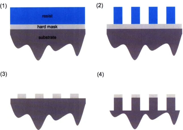
PMMA is notoriously difficult to directly examine in a scanning electron microscope, as it charges and warps before any meaningful measurement can be taken, so any process for measuring PMMA resolution must include a pattern transfer step. Our process, diagrammed in figure 2-14, used PMMA with a molecular weight of 950K to pattern a film of SiOx, which was then used as a hard mask to plasma etch directly into the Si substrate. 30 nm of oxide were evaporated onto a Si substrate, which was then coated with 80 nm of PMMA. The PMMA was patterned with gratings of various pitches and linewidths, then developed for 30 s in 3:1 IPA:MIBK at various temperatures. The PMMA pattern was then transferred into the oxide using a CF4 plasma etch. The
patterned oxide, in turn, was then used as a mask to transfer the original pattern approximately 100 nm into the Si substrate using a Cl2 plasma etch. The result, after
stripping the oxide, was trenches in a Si substrate that were extremely easy to accurately measure in an electron microscope.
(1)
(3)
(2)
(4)
Figure 2-14: Schematic illustration of the two-step etch process used to transfer the
PMMA pattern for SEM analysis. The PMMA is spun onto a Si substrate coated with a
30 nm SiO, hard mask (1). The PMMA is exposed and developed (2), and the developed
pattern is transferred into the SiOx via CF4 plasma etching (3). The hard mask is then
used to transfer the pattern into the silicon via a Cl2 plasma etch (4). The resulting
pattern is much more easily measured with an electron microscope than the developed
2.4.2 Results
As figure 2-15 shows, the linewidths obtained with this process at various development temperatures closely matched the contrast data in figure 2-12. At 15°C, dissolution of partially-exposed material limited resolution and the minimum achievable linewidth was -15 nm. As the temperature was reduced the minimum linewidth decreasee, with the best result (-8 nm) occurring at -15°C. Below -15°C, as with the contrast, the resolution fell off sharply; at -30'C the minimum linewidth was -27 nm, with noticeable sloped sidewalls and footing. It should be mentioned that the minimum pitch achieved in all cases was 60 nm, suggesting that factors besides developer contrast (most likely the mechanical stability of the PMMA during development and etching) limit the minimum achievable pitch in PMMA-based processes.
Figure 2-15: SEM images of 60-nm-pitch gratings developed at 15 C, O C, -15 C, and
-30 °C and etched into a Si substrate, showing the minimum achievable linewidth at each
development temperature. As predicted by the contrast data in figure 5-7, the resolution
improvee as the temperature was reduced, peaked at -15 C, then dropped sharply at
-30 C. The poor line-edge definition and bridging in the -30 C micrograph are
characteristic of sloped resist sidewalls, a symptom ofpoor resist contrast. The "scaly"
coating on the Si in all four micrographs is a 2-nm-thick Au-Pd layer deposited just
before SEM analysis to help reduce charging and had no effect on the process itself
15 C
O°C
-30°C
2.5
Conclusion
Selecting the optimal temperature for PMMA development is a matter of balancing two competing effects. The dissolution of partially-exposed molecular fragments at the edges of features can be reduced by cooling the developer below the fragments' glass transition temperature, but at the cost of reducing the resist sensitivity. If resist sensitivity is reduced too much, the doses required to expose the PMMA will create a large amount of crosslinked material in the exposed region. The presence of these oddly-shaped branched polymers will inhibit the dissolution of the exposed PMMA, resulting in substantial degradation in the contrast. The optimum contrast, then, comes at the temperature where these two effects are minimized; in the case of 3:1 IPA:MIBK developer, this temperature was approximately -15'C. Since different developers change the sensitivity of PMMA quite a bit, this temperature "sweet spot" will vary correspondingly; a naturally insensitive developer (for example, pure IPA) will have a much higher optimum temperature than we observe for 3:1, which is a useful property if the capability to cool liquid to -15°C is not readily available.
We have demonstrated that there is a strong link between resist contrast and real-world lithographic resolution, and that techniques that enhance one will also help the other. By reducing the development temperature of PMMA from 15C to -15°C, we increased the resist's contrast by nearly a factor of two, and achieved pattern-transferred features as narrow as 8 nm. This latter result is comparable to any result achieved to date using
PMMA, including features patterned using much more expensive and sophisticated tools than our Raith- 150.
Chapter 3: Control and Optimization of SEBL Exposure
Parameters
Having investigated one particular example of SEBL resolution improvement via contrast enhancement during the resist development process, we now turn our attention to the actual process of electron-beam exposure-what actually happens to a resist film when energy is transferred into it by an incident electron beam.
3.1
Motivation
There are three major parameters and processes that affect resolution to consider here; effective beam diameter, beam scattering in the resist, and secondary electron generation. A full understanding of all three, as well as how they depend on user-controllable exposure parameters, is essential to finding the true resolution limit of SEBL.
3.1.1 Effect of Exposure Parameters on Resolution
While we have seen in chapter 2 that increasing the contrast of resist can have a marked effect on final resolution, we have not yet considered the contribution of the electron-beam exposure process itself. This is an important oversight, because calculations show that when resist contrast is sufficiently high the point-spread function (PSF) of the electron beam, and not the contrast of the resist, is the limiting factor of resolution, at
least when patterning the complex, arbitrary structures that are involved in most real-world lithographic applications. The limitation of resist contrast when determining final resolution is illustrated in figure 3-1.
wide-PSF narrow-PSF
exposu
I
xposure--- ---- --- ---- resist threshold ---...
Figure 3-1: Energy-deposition profiles for a pattern containing both dense and isolated
features exposed in resist using a wide-PSF beam (left) and a narrow-PSF beam. The
resist contrast here is assumed to be infinite, represented by the "resist threshold" line (anything above the threshold will develop, anything below it will not). In the
narrow-PSF case, both the dense and isolated features are clearly defined and should all resolve
post-development. In the wide-PSF case, however, the dense features are blurred into a
single wide line at the dose needed to expose the isolated feature. Decreasing the dose
(and thus increasing the resist threshold) in order to capture the modulation of the dense
features will raise the resist threshold too high to develop the isolated feature, making it