HAL Id: hal-00395443
https://hal.archives-ouvertes.fr/hal-00395443
Submitted on 15 Jun 2009HAL is a multi-disciplinary open access archive for the deposit and dissemination of sci-entific research documents, whether they are pub-lished or not. The documents may come from teaching and research institutions in France or
L’archive ouverte pluridisciplinaire HAL, est destinée au dépôt et à la diffusion de documents scientifiques de niveau recherche, publiés ou non, émanant des établissements d’enseignement et de recherche français ou étrangers, des laboratoires
Raman study of the CeO2 texture as buffer layer in the
CeO2/La2Zr2O7/Ni architecture for coated conductors
Carmen Jiménez, Tristan Caroff, A. Bartasyte, S. Margueron, Adulfas
Abrutis, Odette Chaix-Pluchery, François Weiss
To cite this version:
Carmen Jiménez, Tristan Caroff, A. Bartasyte, S. Margueron, Adulfas Abrutis, et al.. Raman study of the CeO2 texture as buffer layer in the CeO2/La2Zr2O7/Ni architecture for coated conductors. Applied Spectroscopy, Society for Applied Spectroscopy, 2009, 63, pp.401. �hal-00395443�
Raman study of the CeO2 texture as buffer layer in the CeO2/La2Zr2O7/Ni
architecture for coated conductors
C. Jiménez1, T. Caroff1, A. Bartasyte1, S. Margueron1, A. Abrutis2, O. Chaix-Pluchery1, F. Weiss1
1 LMGP – UMR 5628 CNRS – Grenoble INP –Minatec 3, parvis Louis Néel, BP 257 38016 Grenoble France
2 Departement of General and Inorganic Chemistry - Vilnius University - Naugarduko str.24, LT-03225 Vilnius - Lithuania.
Abstract
CeO2/La2Zr2O7/Ni piled-up structure is a very promising architecture for
YBa2Cu3O7 (YBCO) coated conductors. We have grown YBCO/CeO2/ LZO/Ni
epitaxial structures by metalorganic decomposition (MOD) and metalorganic chemical vapour deposition (MOCVD) methods. The crystallographic quality of the CeO2 layer is
not well determined by conventional X-Ray Diffraction (XRD) due to the superposition of LZO and CeO2 reflections. An alternative simple Raman spectroscopy analysis of
crystalline quality of the CeO2 films is proposed. The F2g Raman mode of CeO2 can be
quantified either by using two polarization configurations (crossed or parallel) or at two different rotation angles around the normal axis (0° and 45°) to obtain information about the sample texture. The sample texture can be determined via a quality factor (referred as Raman Intensity Ratio, RIR) consisting in calculating the ratio of the integrated intensity of the CeO2 F2g mode at 0° and 45° in parallel polarization. This factor
correlates with superconducting performance and can be used as an on-line non destructive method.
1. Introduction
The CeO2/La2Zr2O7/Ni piled-up structure is a very promising architecture for
YBa2Cu3O7 (YBCO) coated conductors. Coated conductors developed by all-chemical
routes are based on the excellent quality of lanthanum zirconate, La2Zr2O7 (LZO), as
buffer layer. Metal organic decomposition (MOD) allows the growth of LZO on Ni-based substrates in reducing atmosphere, which avoids the undesirable oxidation of the substrate. Pyrochlore LZO (Space Group Fd-3m) lattice parameters match these of YBCO (|(εYBCO-εLZO)/εLZO| = 1.05%), and it provides a good barrier against O2
diffusion1,2. This material filling all the characteristics for buffer layers (structural and
chemical compatibility between substrate and active layer) has been already probed as a simple low cost architecture YBCOMOCVD/LZOMOD/NiWRABiTS3. Nevertheless, we tried
to improve the YBCO performance by adding a CeO2 layer grown by MOCVD. The
architecture YBCO (800 nm MOCVD) / CeO2 (120 nm MOCVD) / LZO (80 nm MOD)
/NiW exhibited a higher Jc value (1.2 MA/cm2) than the one-layer buffered structure
YBCO/LZO/Ni (Jc= 0.8 MA/cm2).
The improvement of the YBCO properties by the addition of a CeO2 layer has been
also found by other authors4 concerning the CeO2 and YBCO deposited by physical
methods on LZO buffered tapes and also by Paranthaman et al5 with the more complex architecture YBCO (0.8 µm MOD-TFA)/ CeO2 (60 nm MOD) / LZO (200 nm MOD) /
Y2O3 (10 nm PVD) / Ni , but with very good transport properties (Jc = 2.5 MA/cm2 and
Ic/w= 200 A/cm).
The main factor determining texture as well as physical properties of YBCO layer is the epitaxial and crystalline quality of the CeO2 layer. However, the quality of CeO2
films in the CeO2/LZO/Ni architecture cannot be evaluated by conventional X-ray
Diffraction method due to very similar lattice parameters of CeO2 and LZO films. CeO2
presents a fluorite structure with a lattice parameter of 5.41134 Å, while LZO crystallizes either in pyrochlore structure with a lattice parameter of 10.808 Å or in a disorder fluorite structure with a half value of the lattice parameter (5.407 Å).
In this paper we propose a simple and non-destructive Raman study of the texture quality of CeO2 films based on the variation with polarization of the intensity of the
CeO2 F2g mode in polarized spectra. The ability of Raman spectroscopy to analyse the
in-plane texture of YBCO thin films has been reported since a long time6-9. We show that the texture quality of the CeO2 layer can be determined by the intensity variation of
the first order F2g mode with polarization
2. Experimental
Ni-5%at.W RABiTS tapes presenting a cubic texture were provided by Evico GmbH (Dresden) and described previously10. The full width at half maximum (FWHM) values of the φ-scan (111) reflection (in plane texture) is 6° ± 0.5°, and the FWHM
values of the rocking curve (ω, out-of -plane) of the (002) reflection in the longitudinal
(RD) and transverse (TD) direction with respect to the rolling direction are 5.5° ± 0.3° and 9°± 0.3° respectively. RABiTs tapes also present a small roughness (mean square roughness, rms < 5 nm). The grain size of the substrate is around 50 µm and its thickness is 150 µm. (00l) oriented LaAlO3 (LAO) pseudocubic single crystals provided
Lanthanum zirconate (LZO) was grown on nickel or LAO substrates by MOD according to a procedure previously described11. Lanthanum (III) 2, 4-pentadionate and zirconium (IV) 2, 4-pentadionate were dissolved in propionic acid (CH3-CH2-COOH) to
form lanthanum and zirconium propionates. Propionic acid was added to get a total concentration of cations of 0.6 mol/l. Before deposition, substrates were ultrasonically cleaned in ethanol and acetone during 10 min. LZO films were deposited by dip coating at room temperature in a glove-box. Substrates were immersed for 30 s in the solution and withdrawn at the rate of 6 cm/min. The samples were dried at 80°C under infrared lamps for 60 s inside the glove box. The films were then annealed at 960°C under Ar + 5% H2 gas flow for 30 min.
CeO2 and YBCO layers were deposited by pulsed injection MOCVD on the LZO
buffered Ni tape or LAO single crystal. A single liquid source based on flash evaporation using pulsed injection CVD was used to evaporate the solution. A detailed description of the deposition conditions has been already published 3. The injector sequentially delivered precise micro-doses of metalorganic precursors dissolved in organic solvent: Ce(tmhd)4 in monoglyme, or a mixture of Y(tmhd)3, Ba(tmhd)2,
Cu(tmhd)2 (tmhd = 2,2,6,6-tetramethyl-3,5-heptanedionate) in monoglyme with the
appropriate molar ratio. The flash evaporation of the solution was performed at 280°C and film deposition took place at 750°C for CeO2 and at 800°C for YBCO under a
controlled atmosphere (60% Ar + 40% O2) at 5 Torr of total pressure. CeO2 layers were
deposited with thickness ranging between 30 and 200 nm; YBCO thickness was 600 nm in all cases. The transport properties of the Ni/LZO/CeO2/YBCO layers were evaluated
YBCO layer was chemically removed by dissolution in an aqueous orthophosphoric acid solution (1/10 v/v) before CeO2 layer characterization.
Film texture and epitaxial relations among the different layers were determined by X-Ray Diffraction (XRD) in Shultz geometry using a D5000 Siemens four-circle diffractometer with monochromatic Cu Kα radiation ( =0.15418 nm).
Raman spectra were collected using a Jobin Yvon/Horiba LabRam spectrometer equipped with a liquid nitrogen cooled charge coupled device detector. Experiments were conducted in the micro-Raman mode in a backscattering geometry with a notch filter technology. Spectra were measured at room temperature in air-conditioned room and calibrated using the 520.7 cm-1 silicon Raman peak.
Visible Raman scattering experiments were performed using the TE00 514.5 nm line
of an Ar+ ion laser and a x50 long working distance (LWD) Olympus objective (numerical aperture = 0.5). The laser power was kept at ~ 5 mW at the sample surface on a spot size close to 2 µm. The output light was dispersed on a 1800tr/mm spectrometer with notch filter cutting at ~100 cm-1. In the following, backscattering VV and VH polarized Raman spectra will refer to the polarization of the analyzer parallel (V) and crossed (H) with respect to the incident polarization (V). The direction of the incident and scattered laser beams was normal to the substrate plane.
UV Raman scattering experiments were done at 266 nm wavelength produced from the fourth harmonic of a Nd:YAG laser. Acquisitions were obtained through a x40 UV OFR objective and with an UV extended spectrometer with 2400 tr/mm grating. The notch filter cuts at ~350 cm-1 and no analyzer was used.
3. Results
LZO layers (~ 80 nm thick) were obtained by MOD on LAO single crystal and on Ni substrates. As already reported3, XRD analyses confirm the biaxial texture of the
sample. For LZO layers deposited on LAO, the in-plane texture quantified from ϕ-scans
performed on the (222) reflection was FWHM= 1° and the out-of-plane texture quantified from rocking curves measured on the (002) reflection was FWHM= 0.7°. On Ni-based substrates, LZO out-of-plane orientation was given by FWHMRD=5.3° ± 0.2°
in the rolling direction, FWHMTD=8° ± 0.3° in the transverse direction and the in-plane
texture was such that FWHM=7° ± 0.3. These results confirm that LZO grains have a c-axis orientation and that the LZO film nucleates with a biaxial texture over the substrate with its unit cell axis rotated by 45° with respect to the substrate in both cases (Figure 1).
CeO2 grows epitaxially on LZO, with a cube-on-cube configuration. By XRD, the
crystalline quality of the CeO2 layer can be only quantified by the comparison of the
intensity (counts/sec) of the (400) X-ray reflection for the same sample before and after CeO2 deposition. If the CeO2 layer is not completely textured or polycrystalline, an
additional (222) reflection will be detected at theoretical position of 2θ=28.6° when
using λCu. In the case of partial crystallisation or amorphous state of the CeO2 layer, no
increase of the intensity of the (400) reflection will be measured after deposition. In any case, the systematic measurements of the intensity before and after CeO2
deposition are not compatible with sequential experiments and increase the delay in production of samples. As a consequence, an alternative method is needed to evaluate the texture quality of the CeO2 layer. We will expose now the main principles involved
3.1 Raman selection rules for LZO and CeO2 and texture evaluation
Raman spectra of LZO crystallized in the pyrochlore structure (space group Fd-3m or Oh7) have been reported by Vandenborre12 as well as their mode assignment.
CeO2 presents a fluorite structure lattice (space group Fm-3m or Oh5). Its first–order
Raman spectrum is very simple and consists of a triply degenerated F2g mode at 465 cm -1, assigned to the symmetrical Ce-O stretching mode. The second order Raman
spectrum is more complex and has been reported by Weber13.
The observation of Raman modes strongly depends on polarization selection rules. Considering the polarization directions of the incident and scattered beams, ei and es, respectively, the intensity of the Raman peak F2g is given by [9]:
2 2g , , 2 i (F , ) s Z Y X g F e R e I ∝ ⋅ ⋅ =
γ
γ (1.1)where R(F2g,γ) is the Raman polarizability tensor defined in the cubic crystallographic
coordinate system (X=[100], Y=[010], Z=[001]) as:
⋅ ⋅ ⋅ ⋅ ⋅ ⋅ ⋅ = d d x F2g( ) ⋅ ⋅ ⋅ ⋅ ⋅ ⋅ ⋅ = d d y F2g( ) ⋅ ⋅ ⋅ ⋅ ⋅ ⋅ ⋅ = d d z F2g( ) (1.2)
From the above relations, the intensity of the F2g mode in both LZO and CeO2
crystals will be zero in the VV polarization configuration with VV = XX (or YY or ZZ) whereas it will give a Raman signal in the VH polarization configuration with VH= XY (or YZ or XZ). However, this technique has the disadvantage to depend on the efficiency of the spectrometer in VH and VV configurations.
Another way of varying the Raman intensity consists in rotating the crystal in the (X,Y) plane for a given polarization configuration. Considering the crystal oriented in
the (X,Y,Z) system with the incident beam along Z and (X,Y) the plane of incidence, θ
is defined as the angle between the incident polarization V and the X crystallographic axis of CeO2. The intensity variation of the F2g(z) Raman mode present resulting from
Eq. 1.1 and Eq.1.2 is given by:
2 2 (
θ
) dsin(2θ
) IF gVV ∝ (1.3) 2 2 (θ
) dcos(2θ
) IF gVH ∝ (1.4)Taking into account these equations, in a fully biaxially oriented film, a rotation of the sample around an axis normal to the substrate plane will modulate the intensity from 0 to Imax whereas a sample exhibiting a fibre texture or a polycrystalline sample will
show no modulation at all.
3.2 Raman spectra of LZO and CeO2
The Raman spectra of 160 nm thick MOD LZO films on Ni and on LAO did not show any detectable peak whatever the incident laser light, whereas a strong peak associated to CeO2 peak is detectable even for very thin films (30 nm thick). We deduce
that LZO presents a weak Raman scattering efficiency that is hardly detectable in our thin films. As a consequence, Raman spectroscopy cannot be used to evaluate LZO texture quality and the Raman spectrum of the CeO2/LZO structure did not differ from
the CeO2 film spectrum.
We also studied the CeO2/LZO/Ni heterostructure by UV Raman scattering. The
excitation at 266 nm (above the optical gap of CeO2 at 3.2 eV) results in a strong
absorption of light at the CeO2 surface. The visible and UV Raman spectra confirms that
the Raman intensity result mainly from the CeO2 layer. Nevertheless, these spectra
using UV excitation, higher frequency bands near 600 and 1180 cm-1 were also collected in addition to the F2g mode. They were assigned to second-order features of
CeO2 exalted by the UV laser light (Figure 2). In the following, we will focus on the F2g
mode measured with Ar+ laser excitation.
The CeO2/LZO structure (Figure 3) grows biaxially textured on a nickel cubic
substrate and on (001) LAO, but rotated by 45°. We will define a new reference system (X,Y,Z) made of the geometrical axis of the sample with Z=z normal to the surface and (X,Y) in coincidence with the [100] and [010] directions of the LAO or Ni substrate. On the other hand, the reference system (X’, Y’) for the definition of the Raman tensor taking into account the CeO2 crystal axis used in Eq. (1.2) is rotated by 45° on the (X,
Y) reference system. We will define the rotation angle αs around the normal Z in the
(X,Y,Z) system to be 0° (Figure 2a) in the [100] direction of the LAO substrate or the Ni tape. The rotation angle αs and the θ angle defined in Eq. (1.3) and Eq. (1.4) are related
as follows: αs=θ+45°. This means the F2g mode is Raman active in the parallel
configuration (VV) at 0° rotation angle.
The equivalence between both experimental configurations can be observed for a CeO2-MOCVD (30nm)/LZO-MOD (80 nm)/ Ni structure as shown in Figure 4. First,
spectra were collected at αs = 45°, i.e. in the CeO2 crystal reference system, to obtain
the standard variation of the F2g mode with polarization (Figure 4a). The intensity of VH
spectrum was corrected form the spectrometer efficiency by increasing the acquisition time (x3) in comparison with VV spectrum. The highest CeO2 F2g mode intensity was
obtained in VH spectra for αs = 45° (equivalent to VV αs = 0°) and decreases in VV
spectra for αs = 45°. Then (Figure 4b), spectra were measured in VV polarisation
mode intensity was obtained in VV spectra for αs = 0°. Both series of measurements
give evidence that spectra obtained in VV polarisation at 0° and at 45° contain the same texture information than spectra issued from a change in polarisation configuration, but it is a faster and more direct method.
Some additional Raman modes are also observed in this spectrum. As suggested by the reference spectrum of nickel oxide obtained by thermal oxidation of a nickel substrate in air at 800°C for 5min, they have been identified as NiO modes due to the nickel oxidation through the LZO layer during the MOCVD process.
3.3 Angular dependence of CeO2 F2g Raman intensity
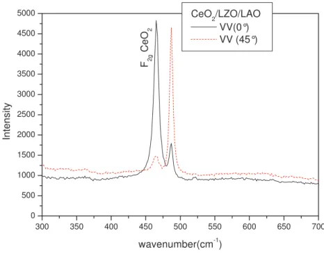
The dependence of the intensity of the CeO2 F2g mode in a CeO2/LZO/LAO sample
has been studied by varying αs in VV polarization configuration. For this experiment,
we have used a CeO2 layer deposited on LZO-buffered LAO instead of Ni substrate to
avoid the NiO signal in the spectrum. Both spectra shown in Figure 5 for αs=0° and
αs=45° correspond to the highest intensity variation. The peak observed at 462 cm-1 is
related to the CeO2 F2g mode whereas the 500 cm-1 one corresponds to the Eg mode of
LAO [14]. Both modes are Raman active in VH configuration, but they appear out of phase due to the 45° rotation between the LAO and CeO2 lattices.
The modulation of the CeO2 F2g mode intensity with the rotation angle, αs, has been
determined by measuring four points at each angle to estimate the dispersion. Peaks were fitted and the integrated intensities thus obtained are reported in Figure 6.The intensity variation with αs follows a cosinus law (or a sinus with θ) as predicted by Eq.
3.4 Raman Intensity Ratio and YBCO performances
To determine the correlation of the CeO2 layer texture with the intensity ratio of the
F2g Raman mode at 0° and 45°, we have defined a Raman Intensity Ratio (RIR) given
by the integrated intensity ratio of CeO2 F2g Raman mode at 0° and 45° in VV
polarization (RIR= IVV(0°) / IVV(45°)). We have studied the correlation of YBCO
performance (Jc values) for several YBCO/CeO2/LZO samples on Ni and on LAO with
RIR. The quality of the YBCO layer was not identical in all the samples, so the Jc values
are strongly dependent on the experiment. Results are summarized in Table I as well as FWHM values obtained from XRD characterizations. A correlation diagram between the RIR and Jc values is presented in Figure 7 for each sample. It is to be noticed that
the number included in the sample label denotes the YBCO deposition experiment; so V19Ni and V19LAO are related to the same YBCO deposition but on two different substrates: the poor Jc value obtained with the LAO sample, correlated to an absence of
texture in YBCO film, can be only explained by a poorly textured CeO2 layer. This is
characterized by a RIR value smaller than 1. On the other hand, the highest Jc values
were obtained for samples with RIR values higher than 2.5.
4. Discussion
Raman studies performed on CeO2 layers have indicated that information about the
film texture can be easily obtained from the F2g Raman mode. This mode does not
overlap with other Raman modes coming from the different materials used in the coated conductor architecture and its intensity is very high, even for very thin films (30 nm thick CeO2, Figure 4). It has also been shown that the biaxial texture of this layer gives
an intensity modulation of the F2g Raman mode when rotating the sample around an
axis normal to the substrate plane; this modulation is not thickness dependent.
Raman spectra obtained in VV polarization configuration at 0° and at 45° rotation angles allow to detect a modulation in the CeO2 F2g mode intensity due to the film
texture. The calculation of the intensity ratio from both spectra allowed to define a quality factor RIR. RIR values higher than 1 attests the biaxial texture of the CeO2 layer.
Otherwise, the buffer layer is poorly or not textured and will not transmit the texture template to the YBCO layer. The CeO2 crystalline quality depends on the crystalline
quality of the LZO surface. Indeed, despite a well-textured structure revealed by the (00l) reflections in their XRD pattern, some LZO layers did not offer a sufficiently high crystalline quality of their surface to obtain a well crystalline contrast in EBSD or by RHEED analyses. Unfortunately, last techniques cannot be routinely used in coated conductor fabrication to qualify the substrates. When using LZO layers as template in next steps, i.e. CeO2 deposition and YBCO deposition, XRD diagrams are no more
accurate enough to evaluate the crystalline quality of the CeO2 layer while the RIR
estimation can give this information before YBCO deposition. Thus, this quality factor can be very useful to qualify substrates for YBCO deposition during the fabrication process.
The collection of the Raman data was performed with using a large working distance x50 objective, which allows the analysis into a small spot (~2 µm) at a relatively long distance from the sample (~2 cm). On the other hand, this analysis is non destructive, rapid and extremely local. It can be performed without sample preparation, at atmospheric pressure, directly or through a quartz window on any substrate shape. All these features indicate that Raman characterization of CeO layer can be used to control
the sample quality in an on-line process or to perform selective tests on sample uniformity.
5. Conclusions
Raman spectroscopy has been used to characterize CeO2/LZO structures with
different CeO2 thicknesses. We have shown that the F2g Raman mode of CeO2 can be
quantified from spectra collected either in two polarization configurations (VV and VH) or at two rotation angles around an axis perpendicular to the substrate plane (0° and 45°) in VV polarization configuration to obtain information about the sample texture. This kind of information cannot be obtained from XRD measurements due to the overlap of the LZO and CeO2 lattices. We have defined a quality factor (RIR) consisting in the
calculation of the intensity ratio of the CeO2 F2g mode at 0° and 45° in VV polarization.
The RIR value quantifies the intensity modulation between both configurations. We have correlated this factor to superconducting performances (Jc). RIR should be higher than 1 to ensure a crystalline quality of the CeO2 layer sufficiently high to template the
YBCO layer. This determination is fast, non destructive and compatible with an on-line characterization during the fabrication of coated conductors.
Acknowledgement
This work has been financially supported by the French Research National Agency (ANR) through the MADISUP Project and by Région Rhône-Alpes SESUC project. We acknowledge Dr Ph. Odier (Institut Louis Néel – CRETA) for fruitful discussions and Dr. M. Decroux (Geneve University) for the collaboration in the Jc measurements.
References
1. W. Seo, J. Fompeyrine, A. Guiller, G. Norga, C. Marchiori, H. Siegwart, J.P. Locquet. Appl Phys Lett 83 , NO 25, 5211 (2003).
2. K. Knoth, R. Hühne, S. Oswald, L. Schultz, B. Holzapfel, Acta Mater, 55(2)
517, (2006).
3. T. Caroff, S Morlens, A Abrutis, M Decroux, P Chaudouët, L Porcar, Z Saltyte, C Jiménez, P.Odier and F Weiss. Supercond. Sci. Technol. 21, 075007, (2008)
4. K. Knoth, R. Hühne, S. Oswald, L. Molina, O. Eibl, L. Schultz, B. Holzapfel. Thin Solid Films 516, 2099, (2008).
5. M.P. Paranthaman, S. Sathyamurthy, M.SZ. Bhuiyan, P.M. Martin, T. Aytug, K. Kim, M. Fayek, K.J. Leonard, J. Li, A. Goyal, T. Kodenkandath, W. Li, W. Zhang, M.W. Rupich, IEEE Trans. on Appl. Supercond. Vol 17 No 2, 3332,
(2007).
6. J.C. González, N. Mestres, T. Puig, J. Gázquez, F. Sandiumenge, X. Obradors, A. Usoskin, Ch. Jooss; H.C. Freyhardt, R. Feenstra. Physical Review B, 70,
094525, (2004)
7. U. Weimer, R. Feile, P. Leiderer, U. Poppe, J. Schubert, J. Fröhlingsdorf, B. Stritzker, W. Zander. Physica C 168, 359, (1990)
8. N. Diekmann, R. Kürsten, M. Löhndorf, A. Bock. Physica C 245, 212, (1995).
9. C. Thomsen, R. Wegerer, H.-U. Habermeier, M. Cardona. Solid State Comm. Vol 83, No. 3, 199, (1992).
10.J. Eickemeyer, D. Selbmann, R. Opitz, B. De Boer, B. Holzapfel, L. Shultz, U. Miller Supercond. Sci. Technol. 14 152, (2001).
11.Z.M. Yu, P. Odier, L. Ortega, L. Zhou, P.X. Zhang, A. Girard Materials Science and Engineering B 130 126, (2006).
12.N.T. Vandenborre, E. Husson, H. Brusset. Spectrochimica Acta, Vol 37A, 113,
(1981).
13.W.H. Weber, K.C. Hass, J.R. McBride. Physical Review B Vol 48, N 1, 178,
(1993).
Table 1
Sample RIR YBCO texture: in plane and out of plane FWHM (°) Jc (MA.cm-2) CeO2 thickness (nm) (103)ϕ (005)ωRD (005)ωTD V13LAO 33 1.5° 0.67° 2.5 30 V13Ni 3.3 8.7° 5° 7.1° 0.1 30 V15LAO 9.6 1.6° 0.55° 0.5 150 V15Ni 1.33 - - - 0.07 150 V17LAO 1.6 - - - 0 200 V17Ni 2.6 8.2° 5.2° 6.7° 0.5 200 V19LAO 0.88 Non-textured 1° 0 60 V19Ni 3.8 7.9° 5.5° 7.5° 0.25 60 V21Ni 5.85 7.7° 5.2° 7.4° 1.2 120 V23Ni 2.6 7.9° 5.3° 7.8° 0.2 60
Figures
Figure 1: Ni and LZO pole figures obtained by XRD on a LZO/Ni sample
200 400 600 800 1000 1200 1400 1600 0.0 0.2 0.4 0.6 0.8 1.0 N iO ? 2nd or de r A1g , Eg , F2g A1g 2nd or de r A1g , E g F2 g N or m al iz ed In te ns ity wavenumber (cm-1) CeO2/LZO/Ni sample
UV laser Ar+ Laser
Figure 2: Raman spectra of a CeO2 layer on LZO/Ni obtained with a UV laser
Figure 3: Schematic representation of the experimental setup.
a) Description of the αs angle used for intensity modulation, which defines the rotation
of the sample around its normal.
b) Polarization configurations in the (X,Y,Z)sample reference system.
c) Representation of the crystal cell of LZO or CeO2 rotated by 45°with respect to the
Ni cell.
b) Polarization configurations
Parallel (VV)
Crossed (VH)
X
Y
Z
z
X’
’
Y’
α
sNi cell
LZO or CeO
2cell
X
Y
Z
X
’
Y’
a) Sample
geometry
c) Epitaxial relation
(00l)200 400 600 0 1000 2000 3000 4000 5000 F2g a) In te ns ity wavenumber (cm-1) CeO2/LZO/Ni VV 45° VH 45° (x3) 200 400 600 0 1000 2000 3000 4000 5000 6000 F2g b) In te ns ity wavenumber (cm-1) CeO2/LZO/Ni VV 00° VV 45° NiO 800°C
Figure 4: Raman spectra of a 30 nm thick CeO2 layer on LZO/Ni.
a) In the CeO2 crystal axis reference system (αs=45°) using VV (solid line) and VH
b) In VV polarisation configuration at αs=0°, (i.e. in the substrate reference system,
solid line) and at αs=45° (i.e. in the CeO2 crystal reference system, dashed line). The
Raman spectrum of a thermal NiO film obtained by direct oxidation of Ni tapes at 800°C is also presented (dotted line).
300 350 400 450 500 550 600 650 700 0 500 1000 1500 2000 2500 3000 3500 4000 4500 5000 F2g C eO 2 In te ns ity wavenumber(cm-1) CeO2/LZO/LAO VV(0°) VV (45°)
Figure 5: Raman spectra of a CeO2 layer on LZO/LAO. The peak near 500 cm-1 is
-20 0 20 40 60 80 100 120 140 160 180 200 0 10000 20000 30000 40000 50000 60000 V15 LAO/LZO/CeO2 F2g in te gr at ed In te ns ity αs (°) Figure 6:
Intensity modulation of the F2g Raman mode of CeO2 (465 cm-1) in a CeO2/LZO/LAO
0 5 10 15 20 25 30 35 V13L AO V13N i V15L AO V15N i V17L AO V17N i V19L AO V19N i V21N i V23N i samples R IR 0 0.5 1 1.5 2 2.5 3 Jc (M A /c m 2 ) I ratio Jc no s up er dc on du ct in g no s up er co nd uc tin g
Figure 7: Correlation diagram between RIR (=I(0°) / I(45°)) and Jc values measured in
samples consisting in YBCO/CeO2/LZO structure. The sample name is relative to the
substrate used and the experiment number for YBCO deposition.