HAL Id: hal-02298409
https://hal.archives-ouvertes.fr/hal-02298409
Submitted on 26 Sep 2019HAL is a multi-disciplinary open access archive for the deposit and dissemination of sci-entific research documents, whether they are pub-lished or not. The documents may come from teaching and research institutions in France or abroad, or from public or private research centers.
L’archive ouverte pluridisciplinaire HAL, est destinée au dépôt et à la diffusion de documents scientifiques de niveau recherche, publiés ou non, émanant des établissements d’enseignement et de recherche français ou étrangers, des laboratoires publics ou privés.
A New Process for the Fabrication of SiC Power Devices
and Systems on SiCOI (Silicon Carbide On Insulator)
Substrates
François Templier, Nicolas Daval, Léa Di Cioccio, Daniel Bourgeat, Fabrice
Letertre, Dominique Planson, Jean-Pierre Chante, Thierry Billon
To cite this version:
François Templier, Nicolas Daval, Léa Di Cioccio, Daniel Bourgeat, Fabrice Letertre, et al.. A New Process for the Fabrication of SiC Power Devices and Systems on SiCOI (Silicon Carbide On Insulator) Substrates. 2002 MRS Fall Meeting, Dec 2002, Boston, United States. �10.1557/PROC-742-K7.9�. �hal-02298409�
A New Process for the Fabrication of SiC Power Devices and Systems on SiCOI (Silicon Carbide On Insulator) Substrates
François Templier, Nicolas Daval1, Léa Di Cioccio, Daniel Bourgeat, Fabrice Letertre1, Dominique Planson2, Jean-Pierre Chante2 and Thierry Billon
CEA-LETI, 17 rue des Martyrs 38054 Grenoble, France
1
SOITEC Silicon On Insulator Technologies, Parc Technologique des Fontaines 38190 Bernin, France.
2
CEGELY, INSA de Lyon, Bat. Léonard de Vinci, 20 avenue Albert Einstein 69621 Villeurbanne, France.
ABSTRACT
Feasibility of 4H-SiC epitaxy on SiCOI substrates has been demonstrated, with high quality of obtained layers. Power Schottky diodes were designed and fabricated on these new structures, and exhibited very interesting electrical performance, particularly in reverse mode, with Vbr ~
1000 V. This technology is very promising for the realization of monolithic SiC power systems.
INTRODUCTION
After years of promising development, Silicon Carbide power devices are now on the potentially high volume market of discrete components, with the first commercially available Schottky diodes. However, the small size, high cost of SiC substrates are still disadvantages which limit fast expansion of such devices. In another hand, in the field of integrated power systems, SiC hasn’t yet emerged. For power systems, SOI (Silicon On Insulator) substrates can be used for the realization of monolithic circuits such as power amplifiers for automotive audio application, with power range up to ~ 100 W [1]. Considering the low breakdown field (0.3 MV/cm) and rather poor thermal conductivity (1.3 W/cm.K) of Silicon, it seems difficult to forecast higher power with this technology.
SiCOI (Silicon Carbide On Insulator) material, made by the Smart Cut process, is a promising substrate for power applications, providing the excellent breakdown field and thermal
conductivity of 4H-SiC, on 4-in. or more wafer sizes, which are silicon line compatible. The first demonstration of a SiCOI substrate was made by LETI in 1996 [2]. This first wafer was followed by an active research in order to recover the semiconductor properties of the transferred SiC layer [3]. Nowadays those improvements allow the fabrication of power devices. Recently we presented the first demonstration of power Schottky diodes on 4” SiCOI substrate [4]. The thickness of the SiC transferred layer is in the order of 0.5 µm. By designing an original structure involving a sloped Schottky contact, we targeted a 600 V / 1A rectifier. After full fabrication of the devices on a 4” silicon line, reverse characteristics with Vbr ~ 300 V were obtained, while
forward current was much lower (~ 1/100th) than expected. This low current was interpreted as the result of failure in the ohmic contact process step. This first achievement was interesting, however we were convinced that the limited thickness of the transferred layer is not intrinsically very favourable for high current densities. In this paper we present an important improvement for the SiCOI substrates, which consist of growing epitaxial SiC layers on top of the transferred layers. We will describe these epitaxies, the design and realization of the first demonstrators of
power Schottky diodes on such structures, which we believe is the first step to high power monolithic SiC systems.
EPITAXY OF 4H-SiC ON SiCOI SUBSTRATES
The CVD process developed here is carried out in an home made cold wall reactor described elsewhere [5]. In the present case, we have used SiCOI substrates with poly-SiC handle
substrate, instead of silicon. The reactants gases are silane and propane mixed in a pure hydrogen carrier gas. Wafers are placed on a SiC coated-susceptor. Growth is undergone at atmospheric pressure and typical growth temperature is 1450°C. Growth rate, doping level and morphology of the epitaxy were compared to those obtained on full 4H-SiC wafers. Prior to growth a slight H2 etch was performed.
Though the high epitaxy temperature, no oxide degradation was observed. Due to the high SiCOI quality, no oxide H2 etching defects were observed unlike what was previously published for
3C-SiC on SOI [6, 7]. Only some voids could be seen (Figure 1). Transmission Electron Microscopy of structures after epitaxy is shown in figure 3.
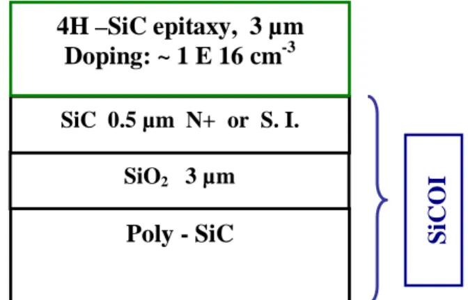
Growth rate, and intentional doping level of epitaxy on SiCOI are similar to those obtained by homoepitaxy on full 4H SiC bulk wafers. With respect to these results the following structures were grown (figure 2). These epitaxies were made for the purpose of evaluating power Schottky diodes (3 µm; ~ 1 ×1016 cm-3) . However, it is important to notice that this is a very versatile technology, as any thickness, any doping type or level, and any combination of epitaxial layers can be chosen. Thus, potentially any kind of device can be made using this technology.
Substrate diameter: Here we have used 2-in. SiCOI substrate, but one should mention that there is no obstacle to make SiCOI substrates using 4-in. (or more) low cost poly-SiC, which provide the wafers to be processed on standard silicon lines. For SiC epitaxy, it is now possible to perform it on 4-in. wafer diameter [8].
DESIGN AND REALIZATION OF POWER SCHOTTKY DIODES
Device structure: Lateral devices were designed [9], giving the schematic structure shown in
figure 4. Edge terminations consist of a B-implanted ring around the Schottky contact. Ohmic contact is made on an N+-implanted area. It is important to notice that after etching SiC layers on the edges, the device is perfectly insulated laterally from others. The anode makes a central electrode, and is surrounded by a ring-shaped Cathode. The main dimensions are listed in Table I. This standard diode is rated for 100 mA in forward bias. Interdigited device with 2 A current rating were also designed.
Influence of doping of the transferred layer: The SiC transferred layer can be chosen among
either N doped or semi-insulating. In the case this layer is N doped at the level of ~ 5 ×1018 cm-3, it will enhance the current flow in the forward mode, but this conducting layer will be
detrimental in the reverse mode because of the shielding of the Resurf effect. By using semi-insulating transferred layer, opposite behaviour will occur with lower On-current and improved reverse mode. As this parameter can have a significant influence on the device characteristics [9], it was evaluated on the devices. Properties of the different transferred layers are described in Table I.
Figure 1. Optical observation of an epitaxy on
SiCOI substrate: only small voids can be seen.
Figure 2. Schematic view of the realized
structures (SiCOI substrate + epitaxy).
Figure 3. Transmission Electron Microscopy on a SiCOI with lower epitaxy.
Buried oxide 3 µm Transferred SiC film 4H SiC, Si face, 0.5 µm N+ doped (~5.1018 cm-3) or: Semi-insulating Epitaxy 4H SiC, 3 µm N- doped ~ 1.1016 cm-3 Diodes: Ring shaped: Interdigited: Length: 21 µm Dimension: 600 x 200 µm Rating: 100 mA Length: 21 µm Dimension: 2000 x 1250 µm Rating: 2 A
Figure 4. Schematic of the Schottky diodes and
substrate structure.
Table I. Main characteristics of the
structures
4H SiC epi
Poly SiC Buried oxide 4H SiC transferred film
Schottky contact Ohmic contact
B implant. (Edge termination)
N implant. Length
4H SiC epi
Poly SiC Buried oxide 4H SiC transferred film
Schottky contact Ohmic contact
B implant. (Edge termination)
N implant. Length Poly - SiC SiO2 3 µm SiC 0.5 µm N+ or S. I. 4H –SiC epitaxy, 3 µm Doping: ~ 1 E 16 cm-3 Si COI SiO2 Transferred SiC SiC epitaxy (bottom part)
Edge termination: Edge terminations were made using B implantation, with an energy of 30
keV and a dose of 1 × 1015 cm-2. Annealing was made at 1050°C. These conditions, which were proposed by Itoh [10], combine rather simple process and good performance. Using this process, the edge termination is effective, by creation of defects [10], and not as a result of p-type-doping, as the annealing temperature (1050°C) is too low for activating B. However, it is important to mention that the using of SiCOI substrates should be compatible with the realization of “true” p-type edge terminations, as these substrates should withstand a temperature of 1500°C, which is suitable for p-type annealing temperature for high performance Schottky diodes [11].
Fabrication of the devices:
The diodes were fabricated using the following process steps:
- Definition of active area: SiC layers are etched at the edges, which allows perfect galvanic isolation between the devices, thanks to the presence of SiO2 from SiCOI
substrate. The etching is made with ICP high density plasma in an Alcatel 601E tool; - Passivation: device are passivated with SiO2 (1.5 µm thick) and, at the end of the process,
with an organic polyimide-like polymer (~ 4 µm);
- Local Nitrogen doping: in order to provide ohmic contact, nitrogen is locally implanted (box profile, 8 × 1019cm-3), followed by high temperature annealing for dopant activation, - Local Boron doping: as it was mentioned above, edge terminations are made by local
implantation of B and 1050°C annealing,
- Formation of ohmic contacts: Nickel is sputtered, patterned and annealed at 950 °C for ohmic contact formation. Prior to metallization, surface is cleaned by dipping in HF, - Formation of Schottky contact: Schottky metallization is made with Ti, which is
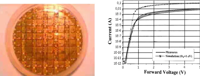
sputtered, patterned and annealed. Both metallizations are reinforced by 1 µm Al layer. The structure is represented in figure 4. A top view of fully processed wafer is shown in figure 6.
ELECTRICAL RESULTS:
Forward bias: Figure 7 shows forward characteristics made on a series of 100 mA-rated diodes,
corresponding to structure with conducting transferred layer. Simulated characteristic is also plotted for comparison. The measured current is lower than expected, around one decade below. The behaviour is the same for diodes made on substrate with semi-insulating transferred layer: for the same size, the current rating is 50 mA, and the measured current is around a decade below expected. We suspected a problem in the ohmic contact, and to verify this we analysed ohmic contact pads by SIMS, after removal of Al top metal layer. The result is given in figure 8. The implanted nitrogen is clearly visible from the SiC surface, and the N signal decreases to the level of the epitaxial SiC drift layer. A significant quantity of oxygen is evidenced at the Ni / SiC interface. We could not determine whether this oxygen was from SiO2 phase, or nickel oxide (or
other), but its unexpected presence was clearly correlated with the failing ohmic contact. This penalising oxygen contamination was attributed to insufficient cleaning of the SiC surface prior to Ni metallization, and/or oxygen leak during the ohmic contact annealing at 950°C.
Contact between Ti and B-implanted SiC: On the wafers we had several TLM test patterns, to evaluate different contacts of the process. We could verify that the Ni / N-implanted SiC contact was very poor (even rectifying). The contact between Ti and B-implanted SiC was also
resistance of ~ 3.5 mOhm.cm² in the best case. This contact should be considered as a contact to
n-type SiC, as the implanted B is not supposed to be activated. This ohmic contact allowed us to
measure the resistance of the SiC layers (transferred layer and epitaxial), and we could verify that, according to doping levels and thicknesses, both SiC layers exhibited non-degraded
resistivities. So we believe that the low On current on the diodes is the result of a failing Ni / SiC ohmic contact, and not due to any SiCOI substrate (and epitaxy) related problem.
Reverse bias: Reverse characteristics were measured. Very high breakdown voltage could be
obtained on the devices. The best results on the SiCOI substrates with semi-insulating transferred layer, this evidencing the Resurf effect predicted by simulations. As shown in figure 9, the Vbr
reaches the very interesting value of ~ 1000 V.
Figure 6: photograph of fully processed 2-in. SiCOI
wafer with epitaxy and devices.
Figure 7: Forward characteristics of Schottky
diode.
Figure 8: SIMS analysis of defective ohmic contact of
Schottky diodes.
Figure 9: Reverse characteristics of
Schottky diode. 1,E-01 1,E+00 1,E+01 1,E+02 1,E+03 1,E+04 1,E+05 1,E+06 1,E+07 0 500 1000 1500 2000 2500 Sputterring time (s) Counts 12C14N 30Si 16O2 58Ni
Finally, the electrical results of Schottky diodes made on SiCOI + SiC epitaxy can be
summarized as follows: (i) the forward current is lower than expected: it was due to accidental oxygen contamination during the ohmic contact step, and is not related to SiCOI substrate and/or subsequent SiC epitaxy, (ii) reverse voltages are excellent, Vbr of ~ 1000 V were obtained, (iii)
the influence of doping of the transferred layer was verified.
CONCLUSION
We demonstrated the feasibility of SiC epitaxy on SiCOI substrates. Epitaxies show very good quality. As a first step for device evaluation of these new structures, we have designed and fabricated power Schottky diodes. Electrical results showed excellent reverse characteristics while the direct current was lower than expected, due to device process problem. Further work is underway to improve the ohmic contact, and demonstrate much higher current ratings, as the current limitation was independent of the SiCOI substrate and epitaxy.
The possibility of SiC epitaxy on SiCOI substrate is open to any doping (type, level) and
thickness, thus almost any kind of horizontal power device can be potentially realized. Moreover, the SiCOI substrate provides the unique possibility of galvanic isolation between device. Overall, we believe that this new technology is very promising for the realization of SiC power systems.
AKNOWLEDGEMENTS
The authors would like to greatly thank R. Madar and I. Matko from LMGP / INPG, for providing TEM characterization.
REFERENCES
1. T. Letavic and M. Simpson, US Pat. 6127703 (2000)
2. L. DiCioccio, Y. Le Tiec, F. Letertre, C. Jaussaud and M. Bruel, Electronics Letters, 32, 12, pp. 1144-45 (1996)
3. E. Hugonnard-Bruyère, F. Letertre, L. DiCioccio, H.J. von Bardeleben, J.-L. Cantin, T. Ouisse, T. Billon and B. Guillot, Material Science Forum Vols. 338-342, 714 (2000)
4. F. Letertre, N. Daval, F. Templier, E. Bano, D. Planson, L. DiCioccio, E. Jalaguier, J.-M. Bluet, T. Billon, R. Madar and J.-P. Chante, Proc. of ECSCRM 2002, Linköping, Sweden, (2002) 5. E. Neyret, L. D. Cioccio, E. Blanquet, C. Raffy, C. Pudda, T. Billon, and J. Camassel,
Material Science Forum Vols. 338-342, 1041 (2000)
6. G. Ferro, N. Planes, V. Papaioannou, D. Chaussende, Y. Monteil, Y. Stoemenos and J. Camassel, Mat. Sci. and Engineerin,g B61-62, 586 (1999)
7. M. Eickchoff, S. Zappe, A. Nielsen, G. Krötz, E. Obermeier, N. Vouroutzis and J. Stoemenos; Mat Sci. Forum, 353-356, 175 (2001)
8. see http://www.epigress.com
9. N. Daval, Etude de la faisabilité de Composants de Puissance sur substrats en Carbure de Silicium sur Isolant (SiCOI), Thesis, November 19th 2002, INSA de Lyon, (2002)
10. A. Itoh, T. Kimoto and H. Matsunami, Proc. of ISPSD 1995, Yokohama, Japan, 101 (1995). 11. R. Rupp, M. Treu, A. Mauder, E. Griebl, W. Werner, W. Bartsch and D. Stephani, Mat. Sci.