HAL Id: hal-00557554
https://hal-iogs.archives-ouvertes.fr/hal-00557554
Submitted on 23 Mar 2012
HAL is a multi-disciplinary open access archive for the deposit and dissemination of sci-entific research documents, whether they are pub-lished or not. The documents may come from
L’archive ouverte pluridisciplinaire HAL, est destinée au dépôt et à la diffusion de documents scientifiques de niveau recherche, publiés ou non, émanant des établissements d’enseignement et de
Structural properties of Al/Mo/SiC multilayers with
high reflectivity for extreme ultraviolet light
Min-Hui Hu, K. Le Guen, J.-M. André, Philippe Jonnard, Evgueni
Meltchakov, Franck Delmotte, Anouk Galtayries
To cite this version:
Min-Hui Hu, K. Le Guen, J.-M. André, Philippe Jonnard, Evgueni Meltchakov, et al.. Structural prop-erties of Al/Mo/SiC multilayers with high reflectivity for extreme ultraviolet light. Optics Express, Optical Society of America - OSA Publishing, 2010, 18, pp.20019. �hal-00557554�
Structural properties of Al/Mo/SiC multilayers
with high reflectivity for extreme ultraviolet light
Min-Hui Hu,1 Karine Le Guen,1 Jean-Michel André,1 Philippe Jonnard,1,* Evgueni Meltchakov,2,4 Franck Delmotte,2 and Anouk Galtayries3
1Laboratoire Chimie Physique – Matière Rayonnement, UPMC Univ Paris 06, CNRS UMR 7614, 11 rue Pierre et
Marie Curie, F-75005 Paris, France
2Laboratoire Charles Fabry de l’Institut d’Optique, CNRS UMR 8501, Université Paris-Sud, F-91127 Palaiseau,
France
3Laboratoire de Physico-Chimie des Surfaces, École Nationale Supérieure de Chimie de Paris (Chimie ParisTech),
CNRS UMR 7045, F-75005 Paris, France
4Now at Institut d’Astrophysique Spatiale, Université Paris-Sud, France
Abstract: We present the results of an optical and chemical, depth and surface study of Al/Mo/SiC periodic multilayers, designed as high reflectivity coatings for the extreme ultra-violet (EUV) range. In comparison to the previously studied Al/SiC system, the introduction of Mo as a third material in the multilayer structure allows us to decrease In comparison to the previously studied Al/SiC system with a reflectance of 37% at near normal incidence around 17 nm, the introduction of Mo as a third material in the multilayer structure allows us to decrease the interfacial roughness and achieve an EUV reflectivity of 53.4%, measured with synchrotron radiation. This is the first report of a reflectivity higher than 50% around 17 nm. Time-of-flight secondary ion mass spectrometry (ToF-SIMS) and x-ray photoelectron spectroscopy (XPS) measurements are performed on the Al/Mo/SiC system in order to analyze the individual layers within the stack. ToF-SIMS and XPS results give evidence that the first SiC layer is partially oxidized, but the O atoms do not reach the first Mo and Al layers. We use these results to properly describe the multilayer stack and discuss the possible reasons for the difference between the measured and simulated EUV reflectivity values.
©2010 Optical Society of America
OCIS codes: (340.7480) X-rays, soft x-rays, extreme ultraviolet (EUV); (230.4170)
Multilayers; (230.1480) Bragg reflectors; (240.6675) Surface photoemission and photoelectron spectroscopy.
References and links
1. T. W. Barbee, Jr., S. Mrowka, and M. C. Hettrick, “Molybdenum-silicon multilayer mirrors for the extreme ultraviolet,” Appl. Opt. 24(6), 883–886 (1985).
2. K. Skulina, C. Alford, R. Bionta, D. Makowiecki, E. Gullikson, R. Soufli, J. Kortright, and J. Underwood, “Molybdenum/beryllium multilayer mirrors for normal incidence in the extreme ultraviolet,” Appl. Opt. 34(19), 3727–3730 (1995).
3. S. Bajt, H. N. Chapman, N. Nguyen, J. Alameda, J. C. Robinson, M. Malinowski, E. Gullikson, A. Aquila, C. Tarrio, and S. Grantham, “Design and performance of capping layers for extreme-ultraviolet multilayer mirrors,” Appl. Opt. 42(28), 5750–5758 (2003).
4. M. G. Pelizzo, M. Suman, G. Monaco, P. Nicolosi, and D. L. Windt, “High performance EUV multilayer structures insensitive to capping layer optical parameters,” Opt. Express 16(19), 15228–15237 (2008). 5. S. A. Yulin, F. Schaefers, T. Feigl, and N. Kaiser, “Enhanced reflectivity and stability of Sc/Si multilayers,”
Proc. SPIE 5193, 155–163 (2004).
6. A. Aquila, F. Salmassi, Y. Liu, and E. M. Gullikson, “Tri-material multilayer coatings with high reflectivity and wide bandwidth for 25 to 50 nm extreme ultraviolet light,” Opt. Express 17(24), 22102–22107 (2009). 7. P. Jonnard, K. Le Guen, M.-H. Hu, J.-M. André, E. Meltchakov, C. Hecquet, F. Delmotte, and A. Galtayries,
“Optical, chemical and depth characterization of Al/SiC periodic multilayers,” Proc. SPIE 7360, O1–O9 (2009). 8. A. Galtayries, M.-H. Hu, K. Le Guen, J.-M. André, P. Jonnard, E. Meltchakov, C. Hecquet, and F. Delmotte,
“Nanometer designed Al/SiC periodic multilayers: characterization by a multi-technique approach,” Surf. Interface Anal. 42(6-7), 653–657 (2010).
9. : J. Gautier, F. Delmotte, M. Roulliay, F. Bridou, M.-F. Ravet, and A. Jérome, “Study of normal incidence of three-component multilayer mirrors in the range 20-40 nm,” Appl. Opt. 44(3), 384–390 (2005).
10. S. Nannarone, F. Borgatti, A. DeLuisa, B. P. Doyle, G. C. Gazzadi, A. Giglia, P. Finetti, N. Mahne, L. Pasquali, M. Pedio, G. Selvaggi, G. Naletto, M. G. Pelizzo, and G. Tondello, “The BEAR beamline at ELETTRA,” AIP Conf. Proc. 705, 450–453 (2004).
11. A. Galtayries, S. Wisniewski, and J. Grimblot, “Formation of thin oxide and sulphide films on polycrystalline molybdenum foils: characterization by XPS and surface potential variations,” J. Electron Spectrosc. Relat. Phenom. 87(1), 31–44 (1997).
12. K. Domen, and T. J. Chuang, “Laser-induced photodissociation and desoprtion. 1. CH2I2 adsorbed on Al2O3,” J.
Chem. Phys. 90(6), 3318–3331 (1989).
13. Y. Mizokawa, K. M. Geib, and C. W. Wilmsen, “Characterization of β-SiC surfaces and the Au/SiC interface,” J. Vac. Sci. Technol. A 4(3), 1696–1700 (1986).
14. M. Yuan, J.-T. Lu, and G. Kong, “Effect of SiO2:Na2O molar ratio of sodium silicate on the corrosion resistance
of silicate conversion coatings,” Surf. Coat. Tech. 204(8), 1229–1235 (2010).
15. S. Tanuma, C. J. Powell, and D. R. Penn, “Calculations of electron inelastic mean free paths. V. Data for 14 organic compounds over the 50-2000 eV range,” Surf. Interface Anal. 21(3), 165–176 (1994).
16. J. H. Scofield, “Hartree-Slater subshell photoionization cross-sections at 1254 and 1487 eV,” J. Electron Spectrosc. Relat. Phenom. 8(2), 129–137 (1976).
17. D. L. Windt, “IMD - Software for modeling the optical properties of multilayer films,” Comput. Phys. 12(4), 360–370 (1998).
18. E. Meltchakov, C. Hecquet, M. Roulliay, S. Rossi, Y. Menesguen, A. Jérome, F. Bridou, F. Varniere, M.-F. Ravet-Krill, and F. Delmotte, “Development of Al-based multilayer optics for EUV,” Appl. Phys., A Mater. Sci. Process. 98(1), 111–117 (2010).
19. P. Jonnard, K. Le Guen, M.-H. Hu, J.-M. André, E. Meltchakov, C. Hecquet, F. Delmotte, and A. Galtayries, “Optical, chemical and depth characterization of Al/SiC periodic multilayers”, Proc. SPIE 7360, 7360O1–7360– O9 (2009).
1. Introduction
In the extreme ultra-violet (EUV) spectral range, the performances of multilayer mirrors are usually limited by material absorption, interfacial roughness and/or surface oxidation. The first experimental reflectivity higher than 50% has been reported by Barbee et al. 25 years ago with Mo/Si multilayers near the Si L edge [1]. Since then, a lot of improvements have been made. In fact, most of the high reflectivity multilayer coatings, as Mo/Si, Mo/Be, Mo2C/Si,
Ru/Be, have been developed for the 11 to 14 nm range, mainly for EUV lithography application [2–4]. Nevertheless, only few results with reflectivity higher than 50% have been reported at higher wavelengths: Sc/Si at 45.9 nm [5] and more recently Mg/Sc/SiC multilayers at 28.4 nm [6]. It is thus required to study new material combinations in order to improve multilayer coating performances in the whole EUV range.
Optical simulations indicate that the Al/SiC material combination could be valuable for applications in the EUV range from 15 to 35 nm. However, Al/SiC periodic multilayers have a large interfacial roughness that leads to low experimental reflectivity. No significant interdiffusion between the layers could be observed using x-ray emission spectroscopy [7,8]. An addition of a thin Mo layer to only the SiC-on-Al interfaces decreases the interfacial roughness and thus improves the optical performances of this system. Moreover, the introduction of a third material in a periodic multilayer structure can increase the peak reflectivity in the EUV range [9].
In this paper, we combine different complementary experimental techniques to study the material distribution within the Al/Mo/SiC multilayers of short and long periods. X-ray reflectivity (XRR) measurements at 0.154 nm (Cu Kα emission at 8048 eV) allowed us to obtain the thicknesses of individual layers and estimate the values of interfacial roughness within the stacks. The optical performances of the new multilayers in the EUV range were tested with synchrotron radiation. Time-of-flight secondary ion mass spectrometry (ToF-SIMS) was performed both to determine the depth distribution (depths profiles) of various elements and identify the chemical composition of a region close to the surface of the samples. We applied the X-ray photoelectron spectroscopy (XPS) in order to determine the chemical state of the outermost 10 nm-thick depth of the stack. A chemical modification of the top SiC layer was of particular interest as this can be responsible for the reflectivity loss in the EUV range.
2. Experiment
Sample preparation and characterization by XRR at 0.154 nm
The Al/Mo/SiC multilayers were prepared by magnetron sputtering in an apparatus described elsewhere [9]. We use a 2 mTorr argon plasma in dc mode for deposition of Mo and rf mode for SiC and Al. All the samples are deposited onto Si polished wafers. The sputtering targets (99.95% or higher purity) are Mo, SiC and Al with 1.5 wt% Si. Indeed, it has been shown by XRR that aluminum thin films including a small amount of silicon are smoother (1 nm rms roughness) than those produced from pure Al targets (2 nm rms roughness). We have selected the multilayers of a short (8.8 nm) and a long (16.6 nm) period with a different number of trilayers. The parameters and the names assigned to the two samples are given below:
Al/Mo/SiC_15: Si / [Al(11.5 nm)/Mo(1.3 nm)/SiC(3.8 nm)]15;
Al/Mo/SiC_25: Si / [Al(6.4 nm)/Mo(1.4 nm)/SiC(1.1 nm)]25 / SiC(1.1 nm).
The Al layers are polycrystalline and the Mo ones are amorphous. Due to the thinness of the SiC layer of Al/Mo/SiC_25, an additional SiC capping layer was added on top of the multilayer. Then, in both samples, the top SiC layer was relatively thick, 3.8 or 2.2 nm, in order to protect the underlying layers from oxidation. The samples were stored in a clean room at 20°C for three months prior to their analysis.
The samples were analyzed by XRR measurements at 0.154 nm (Cu Kα emission at 8048 eV) performed with a grazing-incidence reflectometer working in the θ-2θ mode. The angular resolution is 5/1000°. The dynamic range of a gas-filled detector equipped with calibrated absorption filters is about six orders of magnitude. The XRR curves were fitted in order to determine the parameters of the stacks: the thickness and roughness of their various layers. A simple model of the stack was used for this purpose, i.e. without considering the possible formation of interfacial layers. Since the thicknesses have already been given above, Table 1 summarizes the interfacial roughness of each layer in the stacks.
Table 1. Interfacial roughness values at the three interfaces of the Al/Mo/SiC multilayers derived from the fit of the reflectivity curves measured at 0.154 nm. The values are given
± 0.2 nm Multilayer roughness (nm) Mo-on-Al roughness (nm) SiC-on-Mo roughness (nm) Al-on-SiC Al/Mo/SiC_15 0.7 0.9 0.7 Al/Mo/SiC_25 0.5 0.8 0.6 EUV reflectivity
The EUV reflectivity measurements were performed on the BEAR beamline [10] of Elettra synchrotron facility. The reflectivity curves were measured at near normal incidence (80° glancing incidence) using s-polarized light. The absolute uncertainty of the reflectivity values is less than 0.5%. The photon energy is calibrated with respect to the absorption edges of metal filters installed in the beamline. The intensities of incident and reflected radiation were measured with a solid state photodiode. Incoming photon flux was also monitored by using a gold mesh inserted in the beam path, whose drain current was used for normalization.
ToF-SIMS
ToF-SIMS measurements were performed using a ToF-SIMS 5 apparatus (ION-TOF Gmbh). The working pressure in the chamber was about 3 107 Pa. The total primary ion flux was below 1012 ions.cm2 to ensure static conditions. The depth profiles were measured with the instrument working in the dual beam mode. The sputtering was performed using a 1 keV Cs+ ion beam at a current of 50 nA and rastered over an area of 250 μm × 250 μm. A 25 keV
primary Bi+ ion source (LMIG) at a DC current of 14 nA (high mass resolution mode) rastered over a scan area of 100 μm × 100 μm constitutes the analysis beam. Both ion beams were impinging the sample surface forming an angle of 45° with the surface normal and were aligned in such a way that the analyzed ions are taken from the centre of the sputtered crater.
Since the sputtering yields are not well-known and can vary drastically from one type of ion to another, all profiles are presented as a function of the sputtering time. Only, negative ions were recorded in our measurements. Their signals are intense and rather different from each other. Consequently these profiles are presented on a logarithmic scale. For a given profile, the contrast is defined as the difference between the higher and lower signals with respect to the maximum intensity.
XPS
For XPS characterization, the Si 2p, Al 2p, O 1s, C 1s and Mo 3d3/2,5/2 core level spectra were
recorded using Thermo ESCALAB 250 x-ray photoelectron spectrometer working with a monochromatised focused Al Kα radiation (1486.6 eV) at a pass energy of 20 eV and a take-off angle of 90°. The binding energy scale was calibrated using the binding energies of clean Cu, Ag and Au samples as references. With this calibration, the binding energy of adventitious hydrocarbon contamination is 285.0 eV. The core level spectra were processed with the help of the Avantage program, provided by Thermo Electron Corporation. From the intensities obtained by peak decomposition, equivalent thicknesses of the detected layers were estimated, based on the intensity attenuation (Beer Lambert law) of the XPS signals (see details of the calculation below).
3. Results and discussion
EUV reflectivity
In Fig. 1 we present the EUV reflectivity curves measured at near normal incidence of the two studied samples. High peak reflectivity values are measured: 32.4% at 30.4 nm for Al/Mo/SiC_15 and 53.4% at 17.5 nm for Al/Mo/SiC_25. To our knowledge, this is the first time that such a high reflectivity is reported at this wavelength. They are compared to simulated reflectivity curves expected for ideal stacks, i.e. without roughness and interdiffusion. The high experimental reflectance demonstrated in Fig. 1 indicates the good structural quality of the samples.
Fig. 1. Experimental (bottom lines) and simulated (top lines) EUV reflectivity curves of the Al/Mo/SiC multilayers: Al/Mo/SiC_15 (dotted lines) Al/Mo/SiC_25 (solid lines).
Analysis of the layers within the stack
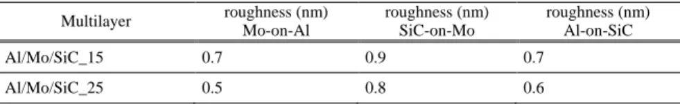
Figure 2(a) displays a schematic representation of the two ultimate periods of the studied stacks. From this scheme, one can understand that ToF-SIMS experiments start with period 1. The depth profile of the Al/Mo/SiC_15 multilayer, which has been sputtered down to the substrate, are shown in Fig. 2(b). For the sake of clarity, we do not show the SiC- and C -profiles since they follow closely the Si- profile. Also, the Mo- profile is not shown at this point and will be discussed later.
Fig. 2. (a)– Schematic representation of the two ultimate periods of the multilayered stack. (b)–
the Si-, O- and Al- ion depth profiles (ToF-SIMS) of the Al/Mo/SiC_15 sample. The numbers 1,
5, 10 and 15 above and below the profiles refer to the Al/Mo/SiC trilayer period as counted from the surface.
The important result is that the 15 different periods of the stack are clearly identified from the periodic modulations of the three selected signals, Si-, Al- and O-. However, the relative concentrations cannot be deduced from the intensities as the ToF-SIMS technique is not quantitative (different sputtering yields are expected with the nature of the elements and the matrix composition). The presence of oxygen is observed at the air/stack and substrate/stack interfaces. The former is most probably due to the atmospheric contamination of the outermost surface layers during transfer and storage in air and the latter corresponds to the native oxide on the silicon substrate. The oxygen within the multilayer, in phase with the Si signals, most probably comes from impurities present in the SiC target. The concentration of oxygen within the samples is very low and this does not impact the optical performances.
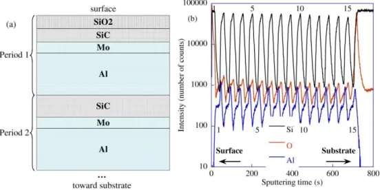
In Fig. 3, we present the depth profiles of the Si-, Al- and Mo- ions from the second, third and fourth periods of the Al/Mo/SiC_15 sample. As previously mentioned, the SiC- follows the Si- profile and is not presented. Only a limited number of periods is considered in order to zoom on the bulk of the stack and to clearly distinguish the shape of the signals. All three profiles have almost the same shape: at the start of a given period, the number of counts increases, then reaches a plateau increases up again to a maximum and decreases toward the start of the following period. Due to the logarithmic scale, the plateau of Si- seems almost as high as the maximum; for Mo-, the plateau is almost seen as a secondary maximum.
As mentioned above, the asymmetrical shape of the SIMS profiles is most probably due to a matrix effect and does not correspond to a gradient of concentration within one period. Due to the thickness of the layers (ultra-thin layers), it is not possible to reach a steady sputtering regime before the end of the period. Large variations of the sputtering yields occur at interfaces (change of matrix) and this leads for example to the sharp maximum of the Al -profile. It is possible to identify the following sequence (from the surface): Si (SiC layer), Mo and Al, thus we have the experimental proof of the expected order of the layers. It is also
worth stating that the depth resolution (expected below 1 nm) allows a satisfactory detection of the Mo layer. By considering that the center of a layer corresponds to the end of the plateau, we can express the position of the layers for period 3 as a sputtering time: 102 s for Si, 108 s for Mo, 130 s for Al.
10 100 1000 10000 100000 50 100 150 In te ns it y (n um ber o f c ou nt s) Sputtering time (s) 2 3 4 Al Si Mo
Fig. 3. The Si-, Al- and Mo- ion depth profiles (ToF-SIMS) of the second, third and fourth
periods of Al/Mo/SiC_15. The Mo- profile intensity has been multiplied by a factor 4 for
comparison. The numbers 2, 3 and 4 refer to the Al/Mo/SiC trilayer period as counted from the air/surface interface.
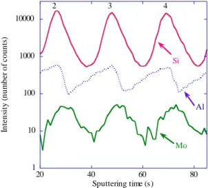
The depth profiles of the second, third and fourth periods of the Al/Mo/SiC_25 are shown in Fig. 4 for the Si-, Al- and Mo- ions. Compared to Al/Mo/SiC_15, the contrasts are smaller because of the lower thickness of the layers (closer to the depth resolution). This time, the Al -profile has a sawtooth shape and the Si- and Mo- profiles are rather symmetrical. However, still considering that the maxima are due to an enhancement of the ion signals at the interfaces (matrix effect) and then estimating the position of the center of the layers not at the plateau (not resolved any more) but in the ascending part of the profiles, we recover the expected order of the layers.
1 10 100 1000 10000 20 40 60 80 In te n si ty ( n u m b er o f c o u n ts ) Sputtering time (s) 4 3 2 Al Si Mo
Fig. 4. The Si-, Al- and Mo- ion depth profiles (ToF-SIMS) of the second, third and fourth
periods of Al/Mo/SiC_25. The numbers 2, 3 and 4 refer to the Al/Mo/SiC trilayer period as counted from the surface.
Analysis of the superficial layers
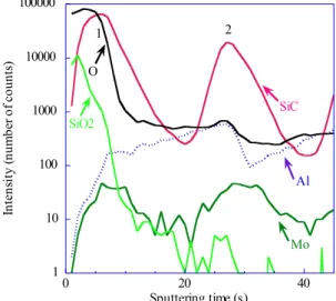
The depth profiles of the SiC-, Al-, Mo-, O- and SiO2- ions for the two ultimate periods of the
Al/Mo/SiC_25 are presented in Fig. 5. Within the first 5 seconds, the SiC- signal reaches a non-negligible intensity. This is most probably due to the formation of an oxide layer on top of the SiC layer. Indeed, in the same set of 5 seconds, the SiO2- and O- signals are intense,
immediately followed by a SiO2- intensity drastic decrease down to the noise level after the
first period. The O- profile confirms the SiO2- intensity variations: the O atoms remain in the
upper part of the SiC top layer. Between 10 and 25 s of sputtering, the intensity of the O -profile remains nearly constant except the small increase periodically occurring in the frame of the SiC layer (oxygen impurities from the target). We also note that the intensity drop of the O- profile (6 seconds) occurs while the Mo- profile reaches its first plateau. Thus, the oxygen diffusion can be limited by the presence of the Mo layer, which acts as a diffusion barrier. This point can be checked with the XPS results. Similar variations were observed with the Al/Mo/SiC_15 sample.
1 10 100 1000 10000 100000 0 20 40 In te ns it y (n um ber o f c ou nt s) Sputtering time (s) 2 1 Al SiC Mo O SiO2
Fig. 5. The O-, SiC-, Al-, Mo- and SiO
2- ion depth profiles (ToF-SIMS) of the first and second
periods of Al/Mo/SiC_25. The numbers 1 and 2 refer to the Al/Mo/SiC trilayer period as counted from the surface.
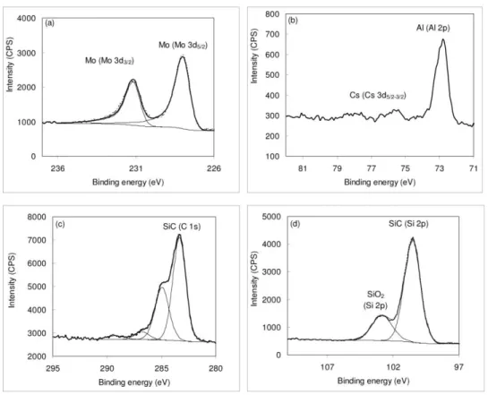
The XPS spectra are performed with the Al/Mo/SiC_15 sample having the thicker SiC superficial layer. Figure 6 displays the core level spectra corresponding to the main elements of the system. The first important result is that it is possible to probe a complete period (period 1) by XPS, until the aluminum layer. The only unexpected element present on the surface is Cs (see the Cs 3d core level on the high binding energy (BE) side of the Al 2p core level). This surface contamination can be explained by a Cs implantation during the ToF-SIMS depth profiling (performed before the XPS analysis).
Fig. 6. Surface characterization (XPS) of Al/Mo/SiC_15. Solid bold line: experiment; solid lines: components obtained from the decomposition of the core level; dashed line: recomposed signal.
By a careful examination of the core level spectra, it is possible to state on the chemical states of the elements present in the more external period (period 1). As regards the Mo 3d5/2
core level [Fig. 6(a)], both its shape (asymmetry of Doniach-Sunjic type) and its BE (227.9 ± 0.1 eV), unambiguously correspond to the Mo metal [11]. This is an important result here to confirm that Mo is not oxidized. The Al 2p core level [Fig. 6(b)] presents only one unresolved doublet (Al 2p3/2-1/2) of low intensity, located at 72.8 ± 0.1 eV, characteristic of metallic
aluminum [12]. The C 1s core level [Fig. 6(c)] presents two main chemical states: the more intense one, located at a BE of 283.3 ± 0.1 eV, is related to carbon in SiC [13] and the second one, located at 285.0 ± 0.1 eV is due to adventitious hydrocarbon surface contamination. Two other contributions of minor intensities (located at 286.8 ± 0.1 eV and 289.2 ± 0.1 eV) are also attributed to surface contamination, corresponding to carbon bound once or twice to oxygen atoms. The Si 2p core level [Fig. 6(d)] exhibits two chemical states. The first component, located at a BE of 100.5 ± 0.1 eV corresponds to bulk SiC [13]. The second one is located at 102.8 ± 0.1 eV and assigned to oxidized silicon SiOx (non stoichiometric silica) and/or
silicates [14]. As regards the O 1s core level (not shown) a symmetrical peak is observed with a maximum at 532.6 ± 0.1 eV that can be attributed to SiOx.
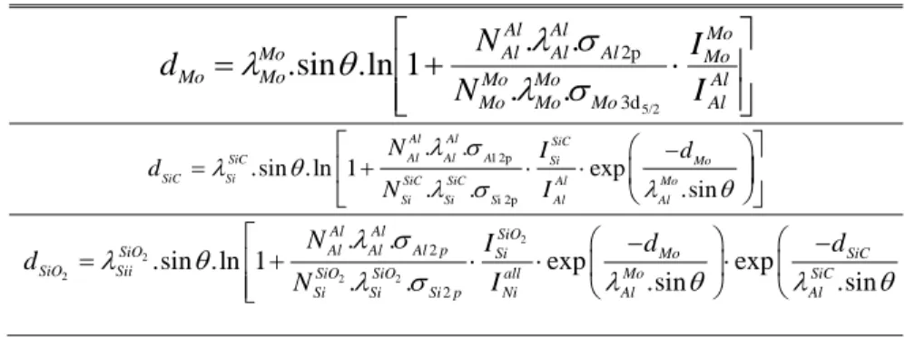
Taking into account the multilayer described in Fig. 2(a), confirmed by the ToF-SIMS depth profiles and assuming a stoichiometric SiO2 in the outermost layer (instead of SiOx), we
have calculated the thickness of the SiO2, SiC, Mo and Al layers in the first period of the
stack. Based on the XPS intensity attenuation of the Al 2p intensity, the equations used for the calculations are given in Table 2. The calculations (considering a 10% of uncertainty) give dMo = 1.5 ± 0.2 nm, dSiC = 6.3 ± 0.6 nm and dSiO2 = 1.6 ± 0.2 nm. These values are in
satisfactory agreement with the expected thicknesses. The values of dSiC and dSiO2 are probably
SiC, the density of which being difficult to estimate (as well as the corresponding inelastic mean free path).
Table 2. Equations of the XPS equivalent thicknesses of the layers in the first period multilayer (period 1) where λ represents the inelastic mean free path (calculated from the
TPP-2M formula [15]), θ the take-off angle, N the atomic density; σ the photoemission cross section [16] and I the peak intensity
Al Al Mo Mo Mo Mo Mo Mo Mo Al Al Al Al Al Mo Mo MoI
I
N
N
d
5/2 3d 2p.
.
.
.
1
ln
.
sin
.
l 2p i 2p . . .sin .ln 1 exp . . .sin Al Al SiC Al Al A SiC Si MoSiC Si SiC SiC Al Mo
Si Si S Al Al N I d d N I 2 2 2 2 2 2 2 . .
.sin .ln 1 exp exp
.sin .sin
. .
Al Al SiO
Al Al Al p
SiO Si Mo SiC
SiO Sii SiO SiO all Mo SiC
Ni Al Al Si Si Si p N I d d d I N
Modelling of the stacks
Theoretical EUV reflectivity curves were calculated using the IMD software [17]. Starting from “ideal” multilayers (no interfacial roughness and no interdiffusion), we modified step by step the modelling of the stack by introducing three effects presented below in order to decrease the simulated reflectivity value toward the measured value. Those three effects are the following:
(1) For the interfacial roughness between the different layers, we use the interfacial roughness values presented in Table 1 and obtained at 0.154 nm.
(2) A 10% reduction of the density of Mo layers is introduced. Indeed, in the reflectivity simulations of Al/Mo/SiC multilayers in Ref [18], such a density reduction has been taken into account for the difference between crystalline and amorphous Mo layers. (3) The oxidation of the SiC top layer is confirmed by XPS and ToF-SIMS
measurements. The present simulations consider for both samples the formation of a 1.6 nm-thick SiO2 layer at the top of the multilayer stack as a result of oxidation:
Al/Mo/SiC_15: Si / [Al(11.5 nm)/Mo(1.3 nm)/SiC(3.8 nm)]14
/ [Al(11.5 nm)/Mo(1.3 nm)/SiC(2.2 nm)] / SiO2(1.6 nm);
Al/Mo/SiC_25: Si / [Al(6.4 nm)/Mo(1.4 nm)/SiC(1.1 nm)]24
/ [Al(6.4 nm)/Mo(1.4 nm)/SiC(0.6 nm)] / SiO2 (1.6 nm).
We do not consider the formation of an interfacial compound at the Al/Mo interface since we have demonstrated [19] that the Al chemical state is the same in the Al/SiC and Al/Mo/SiC systems, indicating that no strong interaction between the Al and SiC layers or between the Al and Mo layers.
To quantify the effect on the reflectivity value of each of the three phenomena listed above, the reflectivity simulations are first carried out considering either the development of interfacial roughness (1), or the reduced density of Mo (2), or the formation of SiO2 top layer
(3). Then, the combined effect of the three modifications (1) + (2) + (3) is calculated. The reflectivity value resulting from each simulation case is presented in Table 3.
Table 3. Comparison of experimental and simulated reflectivity values (R) for Al/Mo/SiC_15 and Al/Mo/SiC_25. Simulation results from individual or combined
simulation case (see text for details)
sample Al/Mo/SiC_15 Al/Mo/SiC_25
wavelength (nm) 30.4 17.5 R (%) exp 32.4 53.4 R (%) “ideal” 44.4 66.2 R (%) / (1) 39.0 61.0 R (%) / (2) 40.3 62.7 R (%) / (3) 43.4 64.6 R (%) / (1) + (2) + (3) 34.8 56.9
The results show that the development of interfacial roughness (1) drastically alters the reflectivity value of the “ideal” multilayer. The Mo density reduction (2) and the introduction of a SiO2 top layer (3) have less effect on the reflectivity value. Finally, the simulated
reflectivity is close to the experimental value when the three effects (1) + (2) + (3) are combined.
4. Conclusion
Periodic Al/Mo/SiC multilayers were studied by combining various experimental techniques providing valuable information on (i) the structural parameters (XRR), (ii) the reflectivity value at the application wavelength (EUV reflectivity), (iii) the depth elemental distribution within the stack (ToF-SIMS) and (iv) the chemical state and distribution of the elements present at the surface (XPS and ToF-SIMS). EUV reflectivity measurements show the excellent optical performance of the multilayers (about 53% at 17 nm). ToF-SIMS depth profiles show the regular succession of the various layers. The XPS analysis demonstrates that SiC in surface of the multilayers is oxidized (about 1.6 nm of SiOx). This oxidation remains
limited in depth and the O atoms do not reach neither the first Mo nor Al layers. A model taking into account the interfacial roughness, the density of Mo thin layer lower than that of crystalline Mo and the 1.6 nm-thick silicon oxidized surface layer, gives EUV reflectivity values close to the experimental ones.
Acknowledgments
Part of this work was funded by the ANR project 07-BLAN-0150. Authors are thankful to Pr. Nanaronne and Drs. Mahne and Giglia from the BEAR beamline for their help during the synchrotron measurements and to Dr. E. Quesnel form CEA for helpful discussion. Multilayer depositions have been carried out on the deposition machine at CEMOX (Centrale d'élaboration et de métrologie des optiques X).