HAL Id: hal-00669515
https://hal.archives-ouvertes.fr/hal-00669515
Submitted on 14 Feb 2012
HAL is a multi-disciplinary open access
archive for the deposit and dissemination of
sci-entific research documents, whether they are
pub-lished or not. The documents may come from
teaching and research institutions in France or
abroad, or from public or private research centers.
L’archive ouverte pluridisciplinaire HAL, est
destinée au dépôt et à la diffusion de documents
scientifiques de niveau recherche, publiés ou non,
émanant des établissements d’enseignement et de
recherche français ou étrangers, des laboratoires
publics ou privés.
Ageing effect on electromagnetic susceptibility of a
phase locked loop
Binhong Li, Alexandre Boyer, Sonia Ben Dhia, Christophe Lemoine
To cite this version:
Binhong Li, Alexandre Boyer, Sonia Ben Dhia, Christophe Lemoine. Ageing effect on electromagnetic
susceptibility of a phase locked loop. Microelectronics Reliability, Elsevier, 2010, 50 (9), p.1304-1308.
�10.1016/j.microrel.2010.07.100�. �hal-00669515�
1
.
.
Ageing effect on electromagnetic susceptibility of a phase-locked-loop
.
B. Li
1, A. Boyer, S. Bendhia, C. Lemoine
.
INSA, University of Toulouse, 135 avenue de Rangueil, 31077 Toulouse, France
.
Abstract
Phase-locked-loop in radiofrequency and mixed signal integrated circuit experience noise as electromagnetic interference coupled on input and power supply which translates to the timing jitter. Most of PLL noise analysis did not take into account the ageing effect. However device ageing can degrade the physical parameters of transistors and makes noise impact worse. This paper deals with the analyses of PLL immunity drift after accelerated ageing.
.
1 E-mail address: [email protected]
1. Introduction
During their lifetime, integrated circuits (ICs) can be affected by failure mechanisms such as electro migration, gate oxide break down or hot carrier injection [1], mainly activated by harsh environmental conditions such as high or low temperature and electrical overstress. Even if failure mechanisms do not compromise the circuit operation, IC intrinsic degradations can have a significant impact on performances, such as noise sensitivity, operating frequency… or Electromagnetic Compatibility (EMC). [2]
The concept of electromagnetic reliability (EMR) [3] has been developed to study and evaluate the impact of circuit ageing on EMC. Analog circuits as PLL are very sensitive to electromagnetic interferences (EMI) [4]. Changes of transistors physical characteristics (such as threshold voltage and mobility) and mismatches due to intrinsic degradations could affect the susceptibility of analog circuits. In this paper, we focus on the evolution of the susceptibility of a CMOS Voltage-Controlled Oscillator (VCO) to EMI coupled on the power supply after accelerated ageing, as power supply fluctuations of VCO is the dominant noise source in PLL. In the section II the principles of EMR characterization is described. EMC measurement methods and accelerated life tests are
given in section III. Section IV presents the device under test (DUT). In the fifth part, the immunity levels measurement before and after accelerated ageing test are compared and the EMI-induced failures are detailed. Finally, experimental results are summed up and discussed.
2. EMR Characterization principles
The characterization of the EMR of a circuit consists in measuring its emission and/or susceptibility level before and after an ageing procedure which accelerates intrinsic degradation mechanisms. As illustrate in Fig.1, it aims at extracting the EMC level drifts induced by ageing as accurately as possible.
Once the EMC and the ageing procedure set-ups have been completely defined, they have to be validated experimentally. The validation step must prove that ageing procedure can only have an impact on the DUT. The EMC validation step must ensure that the EMC measurements are enough repeatable to extract precise information concerning the EMC drifts related to ageing effects. Measurement repeatability and uncertainties set a limit for the consistence of EMC level drifts.
At the end of the measurement campaign, the EMC measurement results obtained before and after ageing are processed to extract statistical data concerning the EMC
2
level drifts, such as the worst case and the mean drifts.These data are required to predict the risk that a component becomes incompliant after ageing and, if necessary, readjust the EMC margins at the design level.
Number of
samples EMC tests Aging stress
Test set-up optimization (Time, cost, accuracy, repeatability) Experimental set-up validation EMC level
measurements Aging stress
Data processing Maximum EMC
level drifts
Mean EMC level drifts
EMC level dispersion drift Individual and statistical analysis
Outputs
EMC failure rate (risk of non compliance for the full lifetime)
Readjustment of EMC margin
Experiments
EMC set-up
validation Aging procedure validation
Fig.1. General description of the electromagnetic robustness of a component
3. Experimental set-up and device under test
3.1. Direct Power Injection Set-up
The direct power injection (DPI) [5] is a standard and efficient method to couple a conducted disturbance to a pin of a circuit (Fig. 2). It consists in superimposing RF disturbances to a low frequency signal through a decoupling network. Uncertainties of the method are acceptable to ensure consistency of EMR results.
Susceptibility is characterized over the band 10 MHz to 1 GHz, the maximum forward power is set to 45 dBm. Three susceptibility criteria are considered: a static margin of the output amplitude set to 20 % of the power supply Vdd, a dynamic margin set to 20% of the output signal period (8ns) and a power current limited to 40 times the nominal current.
Fig. 2. DPI setup, RF injected on power supply rail of VCO 3.2. Burn-in Test Conditions
According to the standard AEC-Q100 [6], accelerated life tests are required to qualify integrated circuits and guarantee the quality and the robustness of
automotive applications. These tests consist in applying an overstress conditions during a short time in order to accelerate the damage rate for relevant degradation
mechanisms. As ICs embedded in automotive
applications often suffer from high temperature, High Temperature Operating Life (HTOL) which consists in applying overstresses conditions.
Ten components are tested and placed during 408 hours in a climatic chamber which regulates the temperature at 150°c +/- 2.5°c. An external source provides a power supply 10% higher than the normal supply voltage. Figure 3 describes the accelerated life test set-up. The HTOL stress mainly accelerates wear-out failure mechanisms as Time Dependent Dielectric Breakdown (TDDB) and Negative bias temperature instability (NBTI).
Fig. 3 Accelerated life test set up
The experimental set-up uses three boards (Tab 1). Dedicated sockets are used on the EMC and ageing boards to move the circuit under test. With this set-up, only the circuits under test are aged.
Table 1 – Three dedicated test boards
EMC board
with a RF Socket to measure
susceptibility level before and after accelerated ageing
Ageing board placed in the climatic chamber with the
sockets special for ageing Monitoring
board
supply and monitor components under test during accelerated ageing
4. Device under test
The PLL is based on a delay controlled ring oscillator designed in 0.25µm SMARTMOS 8 technology from Freescale Semiconductor (Toulouse -
Pforw Prefl DPI Capacitanc Decoupling network Power Supply RF Source Coupler Amplifier Power Meter Current meter Signal Generator Susceptibility Criterion Monitoring Vco Vdd Climatic chamber
Circuit under test Monitoring boards Monitoring with PC Temperature Consumption Output Voltage
3
France), dedicated to automotive applications. The PLLis divided in three sub-blocks: VCO, fraction 1/4 frequency divider and phase comparator. The PLL operates at 24 MHz. Power supplies of these sub-blocks have been separated to identify their own sensitivities to RFI. (Fig.4)
(a)
(b)
Fig. 4.(a) VCO schematic and (b) PLL schematic, it has three separated power rails for its three sub-blocks
5. Experimental results analysis
5.1 Validation of the experimental set-up
First, the repeatability of EMC test bench is evaluated for validation purpose by repeating the measurement 10 times on the same sample. The test bench repeatability is 0.27dB which is highly acceptable since the repeatability errors are inferior to the uncertainty of the DPI test bench, estimated to 2 dB. 5.2 PLL Susceptibility Analysis
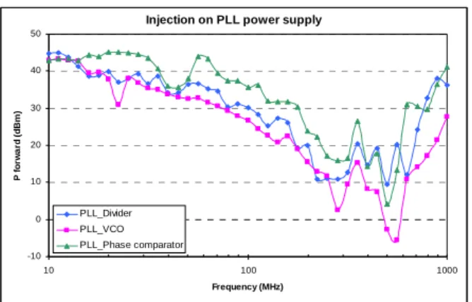
Injection on PLL power supply
-10 0 10 20 30 40 50 10 100 1000 Frequency (MHz) P f o rw a rd ( d B m ) PLL_Divider PLL_VCO PLL_Phase comparator
Fig. 5.PLL susceptibility threshold during conducted injection on power supply pins of the three sub-blocks (Divider, VCO,
Phase comparator)
Conducted EMI injections are performed on the power supply pins of the three PLL sub-blocks. Fig. 5 presents the susceptibility threshold for injection done on three separated power rails: phase comparator, VCO,
and divider.
The comparison among three immunity curves shows that the VCO is the most sensitive block in PLL to the power supply noise.
5.3 VCO Susceptibility Analysis
VCO’s output frequency generally depends on power supply voltage. The variation on power supply can change the propagation delay, thus changing the oscillation frequency in VCO. The sensitivity of VCO to the power supply voltage can be extracted by measuring the output frequency of the VCO for different power supply voltage values (from 2V to 5.5V). Fig. 6 shows the VCO output frequency as a function of its static power supply
VCO output sensitivity
10 15 20 25 30 35 1.5 2 2.5 3 3.5 4 4.5 5 5.5 6
VCO Power supply [V]
V C O o u tp u t F re q [ M H z ]
Fig. 6. Dependence ofVCO output frequency to power supply
voltage.
Any RFI coupled on VCO power supply can modulate the VCO output frequency at the RFI rhythm, resulting in a jitter added to the PLL output signal.
Fig. 7.PLL output signal without (on the left) and with RF injection Without RFI With RFI Phase Comparat or (XOR) VCO Divider 1/4 Vdd1 Vdd2 Vdd3 Fout: 24MHz Fref: 24MHz VCO delay cell Vdd
4
Fig. 8.PLL output spectrum without (on the left) andwith RF injection
Fig. 7 shows the influence of RFI on the VCO output signal and the generation of a jitter. Fig. 8 describes the influence in frequency domain, where many spurious degrade the output signal spectral purity.
PLL output drift with VCO power disturbance
0 5 10 15 20 25 30 0 100 200 300 400 500 600 700
Power supply noise amplitude[mV]
V C O o u tp u t fr e q u e n c y [M H z ] Fmax-Fmin Fmean
Fig. 9.PLL output spectrum without (on the left) and with RF injection
Fig. 9 plots the impact of a RFI on VCO power supply to PLL output frequency. RFI induce a considerable jitter and tends to increase the VCO output frequency.
5.2 PLL immunity Level Drift
With evaluating ageing effect on power supply immunity of three sub-blocks, the perturbation on VCO power supply exhibits a significant evolution of PLL susceptibility threshold after accelerated ageing. Fig. 9 presents the susceptibility threshold of the 6th sample for injection done on phase comparator and VCO power supply pins before and after the HTOL test. The two figures show that VCO immunity is more sensible to accelerate ageing. Its immunity level reduction can reach up to 10 dB over a large frequency range.
PLL susceptibility threshold(Sample6) 0 5 10 15 20 25 30 35 40 45 50 10 100 1000 PLL output Frequency[MHz] In je c ti o n p o w e r o n P h a s e C o m p a ra to r p o w e r ra il [ d B m ] Fresh HTOL 408h (a)
PLL susceptibility threshold (Sample 6)
-20 -10 0 10 20 30 40 50
1.00E+01 1.00E+02 1.00E+03
PLL output Frequency (MHz) In je c ti o n p o w e r o n V C O p o w e r ra il ( d B m ) Fresh HTOL 408h (b)
Fig. 9.PLL susceptibility threshold with an injection on (a) Phase comparator and (b) VCO power rails before and after
ageing
A statistical analysis shows that among 10 samples after HTOL the maximum reduction is 15.88 dB; while the mean reduction for all 10 samples over all frequency is 2.57dB with a standard deviation 3.64dB. Moreover, the process dispersion among 10 samples after HTOL changes from 1.64dB to 4.83 dB.
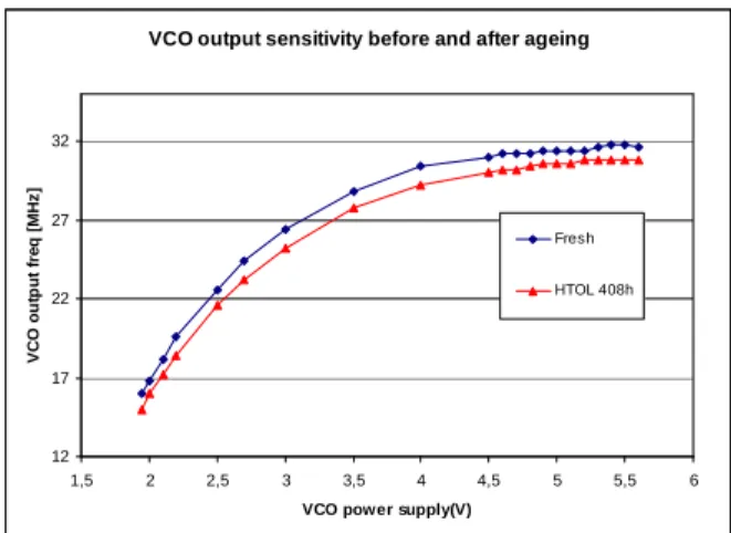
VCO output sensitivity before and after ageing
12 17 22 27 32 1,5 2 2,5 3 3,5 4 4,5 5 5,5 6
VCO power supply(V)
V C O o u tp u t fr e q [ M H z ] Fresh HTOL 408h
Fig.10. Dependence ofVCO output frequency to power supply
voltage before and after ageing
Without RFI With RFI
10dB
Noise frequency: 10MHz
5
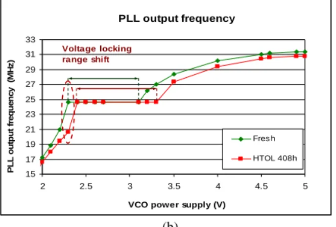
Fig 10 shows after ageing the sensitivity of the VCOhas a drift about 1MHz for each VCO power supply voltage. PLL output frequency 15 17 19 21 23 25 27 29 31 33 2 2.5 3 3.5 4 4.5 5
VCO power supply (V)
P L L o u tp u t fr e q u e n c y (M H z ) Fresh HTOL 408h Voltage locking range shift (b)
Fig.11. PLL output frequency vs. VCO power supply This result indicates that the VCO and thus the PLL becomes more sensitive to power supply fluctuations after ageing. After ageing, a shift of the power supply voltage range ensuring the PLL locking has been measured (fig.11).
6. Discussion
After HTOL ageing tests, the functionality of PLL on all the tested samples is preserved. The current consumption and the performances are unchanged after ageing, proving the excellent robustness of the Freescale
SMARTMOS 8 technology. However,
accelerated-ageing test tends to decrease significantly the immunity levels of VCO and can strongly affect the failure risk of an application which uses this PLL. Moreover, the
dispersions in terms of susceptibility between
components tend to increase after ageing, indicating that the intrinsic degradation mechanisms follow different evolution in each sample. As HTOL mainly accelerates TDDB and NBTI which can degrade transistor parameters, which could constitute the source of the immunity level variation after ageing. For example, the degradation of transistor transconductance (gm) and
mobility (µ) could directly affect the power supply rejection ratio and delay time of gates composing the VCO. Electrical simulations are currently leaded to confirm that the immunity reduction is induced by both a degradation of power supply noise rejection and VCO switching characteristics, provoked by changes of MOS transistor physical parameters. A model including the ageing parameters is going to be studied.
7. Conclusion
In this paper, an original study of the impact of accelerated ageing tests on PLL was presented. The results show that the functionality of circuit was preserved, but the electromagnetic susceptibility of VCO is affected by accelerated ageing test based on high temperature and electrical overvoltage conditions. The immunity level is reduced significantly over a large frequency range, which can increase interference risks with neighbor circuits. The correlation between the immunity level drift and the intrinsic degradation mechanisms needs to be studied in detail to understand the origins of the drift and predict in which extent the susceptibility threshold can decrease.
Acknowledgements
The authors would like to thank Freescale Semiconductor (Toulouse - France) and ESEO (Ecole supérieure d’Electronique de l’Ouest, ANGERS - France) for their technical support and their precious advices. This study has been done with the financial support of French National Research Agency (ANR) and the regional council of Midi-Pyrénées.
References
[1]M. White, J. B. Bernstein, “Microelectronics Reliability:
Physics-of-Failure Based Modeling and Lifetime
Evaluation”, NASA WBS 939904.01.11.10, 2008, nepp.nasa.gov
[2]B. E. Weir et al., “Ultra-Thin Gate Dielectrics: They Break Down, But Do They Fail?”, International Electron Devices Meeting, 1997.
[3]B. Li, A. Ndoye, A. Boyer, and S. Bendhia,
“Characterization of the electromagnetic robustness of a nanoscale CMOS integrated circuit”, EMC Compo 09, Toulouse, France, 2009
[4]J.M Redoute, “Design of EMI resisting analog integrated circuits”, thesis, University of Leuven, May 2009.
[5]IEC 61967, Integrated Circuits, Measurement of
Electromagnetic Emissions, 150 KHz - 1 GHz, IEC standard.
[6]AEC-Q100-Rev-F, Automotive Electronics Council,
Component Technical Committee, Stress test qualification for integrated circuits, , 2003