Design and Fabrication of a
Flexible Membrane Ultrasound Transducer
by
Megan Johnson Roberts
M.S.E., Mechanical Engineering, University of Michigan (2011)
S.B., Mechanical Engineering, Massachusetts Institute of Technology (2008)
Submitted to the Department of Mechanical Engineering
in partial fulfillment of the requirements for the degree of
Doctor of Philosophy
at the
MASSACHUSETTS INSTITUTE OF TECHNOLOGY
September 2018
2018 Massachusetts Institute of Technology. All rights reserved.
Signature redacted
A u th o r ...
...
Department of Mechanical Engineering
Signature redacted
August 10, 2018
C ertified by
...d':'
...
Brian W. Anthony
Principal Research Scientist, Department of Mechanical Engineering
Thesis Supervisor
Signature redacted
A ccepted by...
MASSACHUSETTS INSTITUTE %{ohan Abeyaratne
OF TECHNOLOGY Professor of Mechanical Engineering
OCT 02
2018
Chairman, Department Committee on Graduate Theses
LIBRARIES
Design and Fabrication of a Flexible Membrane Ultrasound Transducer
by
Megan Johnson Roberts
Submitted to the Department of Mechanical Engineering on August 10th, 2018 in partial fulfillment of the
requirements for the degree of Doctor of Philosophy
Abstract
Wearable ultrasound sensing could enable novel medical diagnostics by facilitating continuous, real-time, and direct measurement of physiological phenomena, such as blood pressure. Currently, ultrasound is not used in wearable health sensing applications because clinical ultrasound systems are expensive, bulky, and require high operating power. Realizing wearable ultrasound therefore requires significant reductions in cost, size, and power consumption. Manufacturing cost is of particular concern because sensors are frequently incorporated into consumer goods, where cost is a key driver of technology adoption. Toward that goal, this thesis explored the first steps toward the opportunity to fabricate low-cost ultrasound transducers by contact printing. Contact printing was selected because it could be scaled for high-throughput manufacturing, and it could be performed at ambient temperature and pressure. For this thesis, a capacitive microscale ultrasound transducer was fabricated
by contact printing a gold-parylene composite flexible membrane onto a silicon chip substrate.
Significant challenges with the adhesion between the membrane and the chip were overcome during fabrication process development and a high yield process for the contact printing step was developed. The transducer was characterized for electromechanical performance. The first mode resonant frequency of the transducer was 2.2MHz, with a 2MHz bandwidth, placing it in the range of interest for medical ultrasound applications (typically 1-15MHz). These results demonstrate that flexible membrane ultrasound transducers can be fabricated. Furthermore, they illuminate a path toward wearable ultrasound sensing and more broadly, flexible medical devices.
Thesis Supervisor: Brian W. Anthony
Acknowledgements
Many people have helped me on my path to this degree and their support made it possible for me to accomplish the goal of finishing my PhD.
All three of my committee members provided technical guidance throughout the project.
Brian Anthony gave me the freedom and encouragement to pursue my own research vision. He has supported me through some difficult personal circumstances and I could not be more grateful.
Vladimir Bulovic encouraged me to work with his students and has graciously allowed me to use his lab resources in this project.
Sang Gook Kim has encouraged my interest in micro-nano systems since my undergraduate days and I was delighted to have him on my committee.
The MTL Staff, especially Dave Terry, Dennis Ward, Bob Bicchieri, helped me overcome many fabrication challenges. I am grateful for their expertise and their patience!
My labmates in Brian Anthony's group and technical colleagues from across MIT have been a
source of inspiration and help in a million ways. In particular, I appreciate the input from Jon Fincke, Shawn Zhang, Rebecca Zubajlo, Lauren Chai, Jenny Wang, Mingxiu Sun, Bryan Ranger, and Robin Singh, Katie Smyth, Farnaz Niroui, provided great technical insights that helped in finishing this project. Apoorva Murarka has been a close collaborator throughout the project and taught me a great deal about capacitive acoustic transducers and contact transfer printing.
Sam Young our administrator was critical in helping me order supplies and with other logistical challenges.
Leslie Regan keeps the Mechanical Engineering department's graduate program running and I am forever grateful for her help and her support.
Without Blanche Staton I would not be able to receive this degree. I deeply appreciate her wisdom and mentorship. Patricia Glidden, Tahoura Samad, and Bianca Datta have also been a source of laughter and support.
I have fantastic friends from across MIT and beyond who have supported me through a lot of
personal and professional ups and downs during my PhD!
Nathan Purmort taught me how to design a PCB and encouraged me to climb real mountains on the weekends. I could not ask for a better partner and I'm excited for our future adventures.
Karla Johnson and Stewart Roberts, my wonderful parents, encouraged my curiosity and interest in science from the very beginning. They taught me to work hard and hold myself to a high
standard. Hannah Roberts has been a source of love and support too.
AKC GCH Intl CH Jendu Cela Everlasting Hona Lulu ("Lulu") has been my devoted
companion throughout this journey. Even though she has more prizes and titles than anyone else I know, she still greets me with a tail wag.
Dedication
In 1945, a young woman just 20 years old, took a summer job as a secretary at MIT's Rad Lab. She had studied journalism at University of Kansas and had previously worked as a journalist at Conde Nast as an assistant to the Travel Editor. She was excited with the research advancements happening at the Rad Lab. When she asked to see the nuclear reactor, she was met with skepticism and suspicion. Her name was Marcella Stewart Roberts and she was my paternal grandmother. She returned to Kansas to raise her family but the culture and intellectual energy of MIT left a deep impression on her. Years later when her son, Stewart Roberts, was in high school, she encouraged him to apply to MIT. My father moved to Cambridge and eventually earned two degrees from MIT in Architecture. Grandma passed away while I was in high school, but I know she would be proud of me continuing her legacy as a member of the MIT community.
Meanwhile, during WWII, another young woman in her early twenties was teaching school in Western Ohio. She had just graduated from Bowling Green State University with a business degree. After the war ended, she encouraged her husband, who had dropped out of high school to work on airplanes, to use the GI Bill benefits to attend college and study aerospace engineering. Years later, after she had worked as a teacher for many years, her husband encouraged her to go back to school to advance her career. She graduated from Wichita State with a PhD in Education and became the first female superintendent in the Midwest. Her name is M. Claradine Johnson Allen, (known to her granddaughters as Mim) and she is my maternal grandmother. She passed away while I was in graduate school at MIT. She was proud of all of her granddaughters. She always encouraged my sister and me to pursue our education. She is fondly remembered for giving us math workbooks as birthday gifts.
My mother is the woman who had the biggest influence on me, and the person I most wish could
have seen me finish my PhD. Both she and my dad always taught me to work hard, hold myself to a high standard, and to be humble and respectful of those around me. My mom worked as an architect, specializing in large public buildings including multi-faith sacred spaces, fire stations, and university buildings. She had a wonderful sense of light and flow through a space. She also had a strong empathy and an innate understanding of the people around her.
I am deeply saddened that these three inspiring women are not able to see me finish this degree.
I carry them with me everywhere I go and I know they would be overjoyed to see me reach this goal. It is an honor to dedicate this document to them.
Table of Contents
Chapter 1 Introduction ... 17
1.1 Motivation ... 17
1.2 Wearable and Flexible Sensors for Health Monitoring... 17
1.3 A Brief Introduction to Ultrasound... 19
1.4 Traditional bulk crystal piezo transducers... 21
1.5 Micro-machined Ultrasound Transducers: CMUTs and PMUTs... 23
1.6 Thin Film Acoustic Transducers... 26
1.7 Transfer Printing ... 27
1.8 Commercialization Potential of Wearable Ultrasound ... 28
1.9 D escription of D evice D esign... 31
2 Analytical and Computational Models of the Device ... 33
2.1 Parallel Plate Capacitor M odel... 33
2.1.1 Static Rigid Parallel Plate M odel... 34
2.1.2 Capacitive rigid parallel plate resonator ... 36
2.2 Plate Bending Under Transverse Load... 37
2.2.1 Sm all D eflections... 38
2.2.2 Deflection behavior of a composite membrane ... 41
2.2.3 H ydrostatic pressure... 42
2.2.4 Effective Stiffness of the Membrane ... 43
2.2.5 Large D eflections... 45
2.3 Acoustic Behavior ... 47
2.3.1 Resonance ... 47
2.3.2 A coustic Radiation... 49
2.4 Device Capacitance ... 51
2.5 Finite Element Model ... 55
2.6 Analytical model with the restoring force of the air ... 59
2.7 Summary ... 61 3 Design. 3.1 3.2 3.3 ... Discussion of Customer Needs... Functional Requirements ... Detailed Description of Device Design ... 3.3.1 Material Selection ... 3.3.2 Membrane Design ... 3.3.3 Cavity Diameter and Spacing... 3.3.4 C hip D esign... 3.3.5 W afer D esign... 3.4 Future Design Considerations ... 4 F abricatio n ... 4.1 Silicon Chip Fabrication... 4.2 Composite Membrane Fabrication ... 4.3 Transfer and Adhesion Process... 4.4 Packaging the D evice... 4.5 O ther Fabrication Strategies... 4.5.1 Chip Fabrications Learnings ... 4.5.2 Membrane Fabrication Learnings ... .... 63 .... 63 .... 64 .... 64 .... 67 .... 68 .... 69 .... 72 .... 76 .... 78 .... 81 .... 81 .... 86 .... 88 .... 97 .... 99 .... 99 ... 107
4.5.3 Transfer and Adhesion Process Learnings... 107
4.5.4 PMMA-Gold M embrane ... 110
4.5.5 Parylene side down membrane ... 111
5 Characterization ... 113
5.1 Optical Inspection ... 113
5.2 Electrical Test Set Up ... 119
5.3 Device Failure Mode ... 121
5.4 Electrical Characterization... 122
5.4.1 Electrical Breakdown... 122
5.4.2 Electrical Im pedance ... 122
5.5 Electro-M echanical Characterization... 123
5.5.1 Deflection under applied DC bias... 123
5.5.2 Vibration Response... 125
5.6 Summary ... 132
6 Conclusion & Discussion ... 133
6.1 D iscussion of K ey Findings... 133
6.2 Understanding the stiffness and resonance behavior of the transducer... 134
6.3 Future Work ... 139
List of Figures
1.1 Photographs of a clinical ultrasound machine (a) Shows a photograph of a clinical ultrasound system from GE Healthcare. (b) Shows a photograph of the ultrasound probe, where the transducer elements are at the tip of the probe .... 20 1.2 Shows a schematic of a single element bulk crystal piezoelectric ultrasound
transducer ... 22
1.3 Shows a schematic of a generic CMUT compared a generic PMUT. Both transducer types rely on a movable membrane suspended above a gap (air or vacuum). In a CMUT the membrane moves when an electric field is applied
between the bottom and top conductive electrodes. In a PMUT, a potential is applied across a thin film piezo material, inducing a strain in the membrane and causing it to move ... 24 1.4 A schematic of the Composite Membrane and Chip substrates coming together
to create the device with active cavities ... 29 1.5 A schematic of the chip design, showing major design features... .30 1.6 A photograph of a chip with design features indicated in callout boxes. The
cavities in this chip are 50 tm, and the element diameter is 2.25mm... .30
1.7 A photograph of a device with 25ptm diameter cavities, and a 2.25mm single
element. The printed membrane is visible on top of the chip, as a thin film
(slightly darker gold) on top of the chip ... 31
2.1 Schematic of the parallel plate capacitor model of a simplified electrostatic
d evice.... . ... ... 34 2.2 Schematic of the small deflections plate bending capacitor model of the device. 38 2.3 Shows the difference in deflection based on edge conditions. The disk modeled
here have the same materials, dimensions and applied loads, but differ in their boundary conditions. The simply supported beam's peak deflection is an order of magnitude larger than the clamped edge beam. These were graphed on separate y-axes because when graphed on the same axis, the peak deflection of the simply supported disc is so large compared to clamped, that the clamped
disc would appear as a straight line... . 40 2.4 Calculated maximum deflection of a 1 ptm thick parylene membrane due to
hydrostatic pressure, as a function of the cavity radius. The oil depth was assumed to be 25mm, a typical depth for testing micro-ultrasound transducers. The pull in point is determined by the dielectric thickness and represents an important design constraint. A horizontal line shows an engineering threshold of 3% of the modeled pull in point for a 1ptm dielectric thickness. Based on this estimate, cavity sizes were kept below a radius of 30 Jim ... 43
2.5 Graph showing the relationship between cavity radius and first mode natural
frequency for a 1p rm thick parylene disk, excited by a transverse load ... 48
2.6 Shows a graph of the acoustic pressure over the range away from the wall for a continuous wave ... 51 2.7 Schematic of the capacitance model of the device showing each material and
2.8 Schematic showing the materials and dimension in the COMSOL model. The model was defined as 2D, axisymmetric about the r=O axis. Here, the center of the membrane is at r=0 and the edge of one cavity is at r=25um. ... 55 2.9 A heat map rendering of the z-displacement of the membrane shows that the
deformation is greatest at the center of the device. A top view of a single cavity is shown in (a) and a cross section is shown in (b)... .57
2.10 Graph of finite element model showing deflection profile due to an applied voltage. The x-axis is the distance from the center, where deflection is
maximum. Peak deflection increased with increasing applied voltage ... 58
2.11 Comparison of natural frequency as a function of radius. The solid lines show the analytical model predictions for a plate of either lum thick parylene or 100 nm thick gold. The results from several discrete COMSOL models show that the overall plate behavior has good agreement with the parylene analytical
m o d el... ... ... 58
2.12 Schematic showing that the mechanical restoring force is a combination of the resistance to bending and the resistance to compression of the air ... 59 2.13 A schematic illustrating modeling the air as a compressed ideal gas, compressed
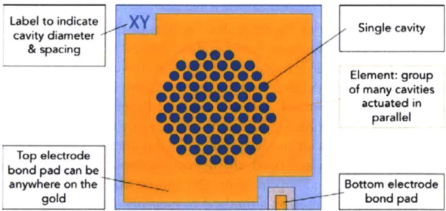
by a piston at one end of a cylindrical volume... 60 3.1 A photo taken of the top view of the device. The circular pattern in the center
is the active area of the device, where the cavity pattern is visible by a texture change in the membrane, appearing in this photo as a dark circle. The gold membrane is visible as the slightly darker gold rectangle at the center of the chip. The membrane is slightly darker because the parylene is on top of the gold. From some angles, the refraction of light makes the membrane appear light pink or light green. The label in the top corner indicates the cavity pattern and spacing of this particular chip. The bottom electrode bond pad is the rectangle on the lower right. The top electrode bond pad can be anywhere on the un-patterned gold surface at the bottom left... 65 3.2 A cartoon cross section of the device showing the chip and the transferred
composite membrane. The bottom electrode is visible to the left and the top electrode bond pad is visible to the right. The four center areas represent four active cavities where the membrane is suspended across an air gap ... 66 3.3 A schematic of the chip design, with call outs for important design features.
This schematic was not drawn to scale. The cavity holes were enlarged to clearly show the difference between a single cavity, and the element (a group of
cavities) ... 66
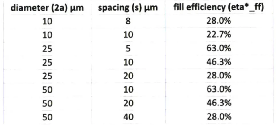
3.4 A drawing showing the cavities arranged in a hexagonal grid, with cavity radius, a, and spacing, s, which are used to calculate by area the proportion of active membrane area inside the active area. The remaining area is used as support
3.5 (a) An image of the AutoCAD layout of the chip. The chip was 12.5mm on a side. In this image, each color outline represents a different mask layer. The pink was Mask A, pattern for etching topside access to the bottom electrode and the diesaw streets. The yellow, Mask B, was the pattern for the chrome gold electrode deposition. Green, Mask C, was the cavity etch and the label indicating cavity diameter and spacing. The cavities were arranged as circles in a hexagonal grid, a close-up of which is shown in (b), where the cavities are
50 tm , spaced 40 pm ... 73 3.6 Photos of failed membrane transfer onto earlier design with more exposed
oxide. In these photos the oxide is the dark area surrounding the large gold circle. The oxide repelled the gold, causing it to roll up and not stick to the chip. This problem was eliminated by minimizing the exposed oxide. The rolling happened immediately after the membrane was cut from the transfer frame (a) and after being totally released from the frame rolls are apparent on all sides of the device (b) ... 75 3.7 A view of the wafer design with each mask shown in a different color. The
white outline represents the 150mm wafer, with the flat shown at the bottom. The pink outline represents Mask A, the yellow is Mask B, and green is Mask C. The mask included patterns for 2.25mm diameter elements and 7mm diameter elements. Inside the element, cavity diameter and spacing were varied in order to quantify the effects of these parameters on the fabrication and function of the transducer. An un-patterned region was left adjacent to the flat for handling the wafer ... 77 3.8 A picture of the three mask designs used in the device fabrication. Mask A and
C are dark field for positive resist. Mask B is light field for negative resist (image
reversal), preferred for liftoff processes ... 78
4.1 Schematic of fabrication process showing a top view and a side view at each step. Each of the numbered steps corresponds to a different photomask. No
photo mask was used for step 1 as it is a blank unpatterned wafer ... 82
4.2 A schematic of the membrane fabrication process, showing the silicon and
oxide layers of substrate, micro-90, parylene and gold, and the peeling step
where the membrane is released from its fabrication substrate... .86 4.3 Photographs of the process for preparing the transfer window. (a) shows the
transfer window after it was cut using a plotter cutter. (b) Double sided tape was applied to one side of the transfer window along its inner edge. (c) shows the transfer window with the tape applied to the inner edge... .89
4.4 Photographs of the process for releasing the parylene-gold membrane from its fabrication substrate. (a) The transfer window was applied to the membrane tape side down. (b) tweezers were used to press down gently on the transfer window to improve the adhesion between the double-sided tape and the membrane. (c) The membrane was peeled from the glass substrate by slowly
pulling upwards with tweezers... . 91 4.5 The composite membrane after being peeled from the oxide substrate, seen
behind it (green). The membrane (gold) is suspended across a polymer transfer window (transparent), which is held by tweezers in this photo. The membrane is 24.9mm on a side ... 92
4.6 The assembly process, which uses acetone evaporation to draw the membrane into close contact with the chip. (a) a droplet of acetone was applied to the surface of the chip. (b) as the acetone droplet dried, the parylene membrane was applied to the chip with the parylene side of the membrane faced up. (c) the membrane was placed on the chip. (d) the acetone begins to evaporate from under the membrane, which was visible under ambient lighting. (e) the acetone has evaporated from roughly two thirds of the chip. (f) The acetone has fully evaporated from under the chip. Small bubbles are visible under the membrane and in the texture of the membrane. At this stage, the membrane can be
repositioned if needed ... 93
4.7 Shows the process for removing the excess membrane. (a) Photo of slicing the membrane around the active area using a thin razor blade. (b) The excess membrane was removed from the device by pulling up on the transfer window with tweezers ... 94 4.8 A photo of several devices after the excess membrane was removed. The
parylene membrane appears as a dark gold region in the middle of the top face of the device. The dark color is due to a thin film optical effect that makes the usually transparent parylene appear greenish or pinkish from certain angles.... 95
4.9 The devices were placed in a foil cup and baked on a hotplate for 30 minutes at
50 C. The temperature was kept low in order not to exceed the glass transition
temperature of the parylene. It was observed that the heat reduced wrinkles and bubbles under the membrane and improved overall adhesion between the two gold surfaces ... 96
4.10 A figure of the simple PCB for packaging the device. The circuitry shown was
intended for electrical impedance matching once the device impedance had been measured. The feature on the left of the PCB is the BNC connector. The grey box on the right side represents a screen print of where the device would
be epoxied. Wire bond pads are present next to the device for robust electrical
connection... 97
4.11 A photo of the complete packaged device showing, from left to right, the BNC
connector, the (unpopulated) impedance matching circuit, the wire bonds, and the device ... 98
4.12 The micro-structure design using the fabrication process described in this section. The layer stack, from the bottom, consists of a doped silicon wafer, an insulating silicon dioxide layer, chrome adhesion layer, and gold electrode layer. 99
4.13 SEM images showing a wafer after 8 minutes of RIE at two different
magnifications. Debris is present all over the wafer, visible on the photoresist
and in the cavity ... 101
4.14 A graph showing etch rates over etch time of each process described in Table
Process Dev. Etch rate was found to be relatively constant over time for wafers with the reduced etch rate, indicating that the issue was not an oxide surface or chrome/oxide interface contamination issue. The etch rate for wafers exposed to chrome etchant was more consistent than wafers not exposed to chrome
etchant ... 104 4.15 XPS data showing that cerium is present on the chip after exposure to wet
4.16 PDMS stamp used for transferring membrane to chip. In this case the chip had already been assembled onto the PCB, as shown in (a). This image shows the aftermath of the membrane being pulled from the glass substrate and then a PDMS stamp was used to push the membrane into the chip. The membrane preferred to stick to the PDMS stamp, and came with the stamp when the
stamp was removed. (b) micro-wrinkles are visible in the gold adhered to the
PDMS stamp ... 109
4.17 Shows the process for creating the PMMA membrane. (a) Shows a schematic of the layer stack of the membrane. (b) is a photograph of the substrate in a
saturated NaOH solution, used to release the PMMA membrane from the silicon substrate by dissolving the oxide layer. (c) shows a device with a PMMA membrane. Wrinkles and tears are visible on this device ... 110
4.18 A side by side comparison of a COMSOL model shows that for a given electric
potential and membrane dimensions, the peak deflection of the parylene is
slightly higher than the PMMA device... 111 4.19 Shows the z-displacement of the membrane using a finite element simulation,
using the same dimensions as the COMSOL model described in Chapter 2. It was shown that the membrane would deflect only a peak deflection of 12nm under a 100V bias, which was determined to be not sufficient volumetric
displacem ent for acoustic output... 112
5.1 Shows nine devices after membrane assembly and annealing. Different lighting conditions were used to capture these photos, which accounts for the variation in color of the device. Each device was 12.5mm on a side. The upper left corner of each device was labeled with its cavity diameter and spacing between cavities, in microns. The smallest diameter cavities (10 tm) had no bubbles and the membrane was flat. It was only possible to see the underlying cavities with precise lighting which allowed light to transmit through the parylene and thin gold layer, revealing the underlying substrate. The medium diameter cavities (25 tm) were also flat. One device had large bubbles (500pm-lmm diameter) spanning many cavities. The largest diameter cavities (50ptm) exhibited a combination of large bubbles, bubbles in a single cavity, flat areas, and sunken-in conditions. A gradient of flat area to small bubbles to large bubbles was visible on some devices, suggesting that the timing of evaporation and laying
down the membrane affects the resulting membrane morphology ... 114
5.2 Shows a device with many of the features observed after assembly. There are several large (>500tm) bubbles present on the device that span many cavities,
such as the one outlined in the blue square. There is also a region on the upper right where there are many bubbles that span only a single cavity. In these, the membrane is in fact taller than the substrate because there is air trapped inside which pushes the membrane upwards away from the cavity. In the lower left, where the purple box is located, there is a large region where the membrane appears to
lie
flat on the cavities. It is possible to see through the thin gold layer to the underlying chip substrate, but there are not shadows to indicate that the5.3 Two devices with the same cavity diameter and element diameter are shown side-by-side to compare the morphology of the membrane. (a) the membrane had completely collapsed into the cavities, so the device was non-functional. (b) each cavity has a bubbled membrane, and some bubbles span 2-4 cavities. This device was functional. (c) shows a magnified view of the collapsed membrane.
(d) shows a magnified view of the element where under the membrane each
cavity contains a sm all bubble... .. 118
5.4 Shows a block diagram illustration of the driving electronics of the transducer. . 119 5.5 A bias tee was used to add the AC and DC signals. photo of the custom
bias-tee attached via BNC connection to a device. The toggle switch was used to
safely discharge the capacitance of the device when powering down ... 120
5.6 A graph of the AC magnitude voltage coming out of function generator as
compared to the AC voltage coming out of the Bias Tee with 50V DC bias .... 121
5.7 Shows the magnitude of the impedance over the frequency for a 40V DC offset and a 500mV AC signal. The device behaved as a standard capacitor for this excitation signal, because the AC signal was not strong enough to excite the
membrane ... 123 5.8 Data from an optical profilometer measurement to characterize the deflection
of the membrane under an applied DC bias voltage. (a) shows the surface height under no DC bias and 130V DC (the maximum applied load). A black arrow indicates a single cavity with a bubble formation under the membrane. The magenta arrow points to a cavity with a flat membrane. (b) shows the center point z-direction deflection of the membrane under a range of applied loads. As expected, the displacement increased with increasing voltage. The flat membrane cavity, however did not show as strong a trend toward increasing
deflection as was expected ... 124
5.9 The relationship between coupling coefficient, k' , and applied DC voltage. The maximum coupling coefficient was .25 for both the flat membrane and the bubbled membrane. The colors match the arrows in Figure 5.8. Coupling coefficient increased for increasing DC bias. Above the 130V DC load, the
device shorted and no measurement was taken ... 125 5.10 A device was driven with a DC offset 28.7V and AC magnitude of 7Vpp. First
a continuous 1MHz sound wave signal was chosen and (a) shows the time response and (b) shows the frequency domain response. Vibrometer
measurement was sampled at 50MHz. This experiment verified that the device responded to a periodic electrical stimulus with a corresponding mechanical
vibration response ... 126 5.11 The device was excited with a 50V DC bias, and a delta function of varying
magnitude, where (a) shows the time domain signal. The magnitude of the mechanical response to the magnitude of the electrical input was linear, as
show n in (b)... 126 5.12 The vibration response of a device (a) was measured in two locations. A
magnified view of the element is shown in (b) with arrows indicating the two areas: one where the membrane was flat across the cavities, and one located on top of a large bubble. The time domain response (c) and the frequency domain response (d) of both locations were compared. It was possible to actuate the bubble. The magnitude of the response in the flat area was greater than on the
5.13 Two devices were excited with 50V DC and a 200ns delta pulse of 30V magnitude. Device A was a 2.25mm diameter element with 50um diameter cavities spaced 50um. Device B was an 8mm diameter element with 50um
diam eter cavities spaced 20um ... 128
5.14 Still images from the animation showing the peak displacement under 50V DC
and 10V AC input. (a) shows a top view of the vibrating membrane and (b) shows a side view. This data indicated that at 2MHz, the membrane was
vibrating in its first m ode... . 129 5.15 Schematic of experimental set up to measure the bandwidth of the transducer. . 130 5.16 Device 9 under a 30V DC bias plus a 1OVpp AC. The resonant frequency was
2.2 MHz bandwidth of this device was 2.03 MHz, which led to a
Q
factor ofapproximately 1, indicating the system is under damped ... 131 5.17 Device 6 under a 30V DC bias plus a 1OVpp AC. The resonant frequency was
2.6MHz, with a bandwidth of 1.4 MHz, which lead to a
Q
factor ofapproximately 1, indicating the system is under damped ... 131
6.1 SEM images of the active cavities, in increasing magnification. (a) shows the
entire element. (b) shows a few elements, where it is apparent the chrome gold top layer is over-etched relative to the underlying oxide. (c) a top view of the edge of the cavity, where the light grey is the gold, over-etched by
approximately 2jim relative to the diameter of the oxide etch. The textured alumina is visible at the bottom of the cavity. (d) shows a tilted side view cross section is shown to show where the metals on top of the oxide are etched... .135
6.2 A graph of the shape function of the clamped edge (r=a), the over-etched
clamped edge (r-a+e), and the simply supported edge (r=a) for a 50tm
List of Tables
2.1 Shows design parameters of each chip design on the wafer ... 53
2.2 Material properties for commonly used MEMS ultrasound transducer membranes. The ratio of E/(1-nu2) was calculated for these materials, indicating a two order of magnitude difference for soft polymer materials
compared to rigid crystalline materials... 54
2.3 The parameters used for the COMSOL model. 56
2.4 The linearized membrane stiffness and natural frequency of the three different cavity diameters, compared with the air spring natural frequency ... .60
3.1 Cavity diameters and their predicted resonant frequencies. Resonant frequencies were chosen to fall in the medical ultrasound range. The cavity diameters were intended to also explore the fabrication process. This
calculation does not consider damping from the coupling medium ... 69 3.2 Several combinations of cavity diameter and spacing were explored and
compared for their fabrication limitations as well as their fill efficiency ... 71
4.1 Process undertaken in MTL - TRL on a 150mm silicon wafer with up to 1 micron of thermal oxide on the polished side. This chart shows the machines
used and the order in which they were used ... 83
4.2 RIE recipe used to etch silicon dioxide in a LAM 590 in a mixture of CF4/CHF3. Step 3 is the etch step and the time for this step was varied
depending on the thickness of the desired oxide etch... 85
4.3 A chart showing the knockout processes used to determine the root cause of
the reduced RIE oxide etch rate. Each wafer was given a name (e.g. Al) to
facilitate keeping track of processes and results ... 103
4.4 Shows the chemistry of each of the wet chrome etchants (as published by their suppliers) used in the etch process development. The oxide etch rates of wafers exposed to either of these chrome etchants were essentially the same, indicating that the ceric ammonium nitrate was the cause. (Water had previously been eliminated as a suspect by exposing a wafer to water and then etching oxide in
R IE ) ... .... ... 10 5 5.1 Shows a comparison of excitation signal, measured displacement, and the
corresponding COMSOL modeled displacement for that excitation signal ... .130
6.1 Numerical values for the clamped edge condition and the simply supported
edge condition for each cavity diameter ... 137 6.2 Numerical values for the predicted resonant frequency of the clamped edge
Chapter 1
Introduction
1.1 Motivation
In parallel with advances in wearable health monitoring, recent advances in medical ultrasound have made the technique more useful than ever before for probing inside the human body. Ultrasound imaging has been around since the mid-twentieth century, but advances in computer science and miniaturization of electronics have led to improvements in resolution, quantitative measurements of tissue health, such as blood pressure [1], [2], muscle[3], [4], and liver[5], [6]. These techniques allow healthcare providers to probe the human body for deeper understanding of disease, with minimal risk to the patient, and at a lower cost compared to other medical imaging techniques.
Ultrasound would be an ideal sensing modality for wearable health because it is safe and non-invasive. Ultrasound is not available as a wearable sensing technique because the
transduction methods currently requires AC Mains wall power, cost hundreds of dollars, and are only beginning to become small enough to be considered portable devices. A wearable device would need to be even smaller. Micro-ultrasound transducers have demonstrated improved resolution over traditional bulk piezo transducers, especially at shallow tissue
depths and specifically have been used to image the carotid artery [7], [8]. Previous research used ultrasound images of the carotid artery in combination with information about
externally applied pressure to accurately measure patient blood pressure[1]. In order to combine these fields, it is necessary to build ultrasound transducers that require lower power and can be formable around the complex curves of the human body.
1.2 Wearable and Flexible Sensors for Health Monitoring
Wearable sensors are undergoing rapid innovation and there is significant interest in personal health monitoring. Throughout human history, people have worn talismans and charms with the promise that their use will improve health. Eye glasses, one of the earliest wearable medical devices, have been used for over 700 years[9]. Similarly, hearing assistant devices have been in use for centuries, and more recently, electronic hearing aids are worn discreetly by many people.
In the last decade, wearable health monitoring has gained popularity alongside advances in portable consumer electronics, especially mobile phones. A savvy consumer can now be outfitted head-to-toe in wearable sensors: in a football helmet (Riddell), earbuds (Dash), on
the wrist (Apple Watch, FitBit, Misfit), in a ring (Motiv), in a bra (Bloomer Tech), in a baby onesie (Mimo sleep and activity tracker by Rest Devices), on a strap around the thigh (Humon), and in shoes (Nike, Underarmour), among others. Readily available consumer wearable devices generally measure activity through indirect metrics. One common method of measuring physical activity is through micro-accelerometers embedded in a wearable device such as a watch or a shoe.
Direct non-invasive measurement of biological data is a small yet growing field. Current commercially available wearable devices and devices in development can measure heart rate
(Fitbit, Apple Watch), pulse oximetry, skin temperature, hemoglobin saturation in muscles (Humon). Within the clinical data space, rudimentary 2-lead electrocardiogram (EKG) for atrial fibrillation detection is available as an adapter to a smart phone or smart watch adapter
(AliveCor). Similarly, a different company has developed a glove intended to be worn by first responders to measure the EKG of a patient (ECGlove). One wearable device with FDA approval comes in several forms, such as a blanket or vest, with inflatable air pockets designed to move fluid out of extremities of patients as a treatment for lymphedema
(Flexitouch Plus).
One of the big questions in this space is whether more information leads to better health outcomes. For example, there is little data to suggest simply collecting activity data leads to weight loss. Some research has shown that behavioral interventions based on data from activity monitors like FitBit can be used to slightly improve activity levels in adults[10], [11]. This question is an active area of research. More information about the types of
interventions that result in measurable health outcomes is needed in order to maximize the utility of wearable health monitoring[12].
Wearable health sensors occupy a challenging commercial space. On their own, they have more in common with diagnostics than therapeutics. Additionally, there is potential for wearable sensing to be incorporated into a therapeutic feedback loop which may in turn enable better therapies. Already, in Type-1 diabetes, there has been clinical and commercial success in wearable continuous glucose monitoring. This strategy continuously measures the patient's glucose levels and then communicates with an insulin pump to calculate and deliver the appropriate insulin dosage in nearly real time. The benefits are significant: both narrower control of insulin levels and significantly reduced need for the patient to interact with the insulin pump to deliver an appropriate dose. This is a critical improvement to patient care in Type-1 diabetes. There may be potential for this closed-loop diagnostic-dosage therapy approach to be applied to other diseases as well. The move towards these closed-loop therapies is likely a long-term direction for wearables and will require significant technological advancement in safe real-time physiological sensors.
One use that may see early commercial success is wearable sensors for clinical trials. A significant financial incentive exists for therapeutics companies to collect reliable data to demonstrate drug efficacy to regulatory bodies. Today, many clinical trials depend on subjective measurements, such as asking the patient how he feels or qualitatively observing
his behavior. Obviously, many factors may affect these subjective measurements, such as patient mood, hydration, or clinician-patient interaction. It is nearly impossible to control for all of these factors as part of the clinical trial design, and indeed many clinical trials fail because the variance in the data collection is relatively high. This challenge is well known in
clinical trial design, but clinical trials are usually limited to taking measurements that are minimally invasive and focused on patient outcomes. There could be enormous benefit to the drug & biologics industries to expand available methods for directly measuring
physiological phenomena outside the clinic and across a greater time scale. For systems with noisy data, signal processing engineers deploy systems which average over many
measurements in order to improve the signal to noise ratio. This approach has not been applied to clinical trials yet because this field needs better and more specific measurement techniques.
There has been much interest in building flexible devices for medical sensing[1 3], [14]. Specifically, a few research teams have explored the opportunity to embed piezo material in flexible polymer such as PDMS in order to build flexible pressure sensing arrays [15], [16] or to attach piezocrystals to polyimide for ultrasound arrays[17]. Additionally, bulk PZT has been placed across a polyimide film and encapsulated in PDMS in order to be incorporated into a flexible ultrasound array[18]. Interest in transducer miniaturization and packaging on flexible electronic circuits is of interest for clinical applications with small geometry, such as intracardiac imaging for applications such as atrial fibrillation [19]. These advances in miniaturization and flexible circuits may enable new diagnostics and therapies. It has been shown that the immune response of cells to implants or foreign materials is effected by material properties such as stiffness, texture, or surface chemistry[20]-[22]. As ultrasound is miniaturized, and in implantable applications are explored, there may be increasing interest in flexible ultrasound for long term direct interfacing with biological tissues.
1.3 A Brief Introduction to Ultrasound
Ultrasound has been used for medical imaging for decades and has been described in great detail elsewhere[23]. At its most basic level, ultrasound works by sending an acoustic wave into a medium, and listening for reflected waves. A sound wave is a traveling localized compression of the medium. Within the medical space, ultrasound is most familiar as an imaging technique, particularly for fetal imaging and echocardiogram (real time imaging of the heart and blood flow).
The hospital grade clinical ultrasound system consists of the probe which sends and receives the acoustic signal, the electronics for signal processing, and a screen for displaying the image and clinical data, as shown in Figure 1.1. Screens and computational electronics have already been miniaturized & commercialized by the consumer electronics industry. Therefore, a move towards portable or wearable ultrasound must focus on miniaturization
I-. I
~
a(a) (0)
Figure 1.1 (a) Shows a photograph of a clinical ultrasound system from GE Healthcare. (b) Shows a
photograph of the ultrasound probe, where the transducer elements are at the tip of the probe.
There are many advantages of ultrasound. It is safe, low cost, non-invasive, and can generate real time images and videos. Unlike magnetic resonance imaging (MRI), x-ray, and computed tomography (CT) scans, there is minimal risk associated with harmful contrast agents or radiation. Traditionally these other methods were associated with higher imaging resolution, however advances in image processing have improved the resolution to where systems have demonstrated 86pm resolution[24]. Additionally, ultrasound can be used to measure blood flow through Doppler[23], blood pressure[I], and tissue stiffness through elastography[23]. Ultrasound is also no longer limited to 2D images. State of the art clinical systems are able to create 3-dimensional real-time images[25], [26].
One of the clinically relevant limitations of ultrasound is that it is nearly impossible to reproduce a scan even when performed by a skilled operator [27]. Therefore, ultrasound
to enable clinical decisions and interventions. The lack of reproducibility is inherent to the way the image is captured. Typically, the sonographer applies the probe to the surface of the body and takes a sonograph, essentially a reflection-field picture of a slice of the body. Because the probe is not fixed relative to the body, it is able to freely rotate and translate. Additionally, the contact force between the probe and the body is not controlled. Therefore, these sources of variation make exactly reproducing an image essentially impossible for a hand-held probe.
Some progress has been made in the development of "hands free" ultrasound systems. Several strategies have been considered. One strategy is to use conformal
transducers that can match the contours of the body. Proposed ultrasound devices in this area[16], [25], [28] generally consist of piezo crystals embedded inside a silicone media, which is soft enough to conform to the skin. Another strategy is to use lasers [29]-[32] to use optoacoustics to locally generate a sound wave in the tissue and precisely measure reflected tissue vibration on the skin surface.
A lightweight flexible ultrasound patch that could be applied directly to the skin
would eliminate the variability from a hand-held probe, because it would not need to be applied with significant force and would be fixed to the body. Further, if the patch consisted of a 2D element array, it could create a 3D volumetric image, which would eliminate the variability based on the probe position. These images could then be acquired in a
reproducible way. Subsequent images could be compared to evaluate changes in tissue health over long time periods. Monitoring changes in tissue health is increasingly of interest for slow growing tumors or evaluating disease progression for degenerative diseases such as muscular dystrophy. An inexpensive, non-invasive, and safe way to take repeated measurements over the course of years is of great clinical interest.
A small, thin, and flexible patch may open up new clinical imaging areas that are
currently not possible or are currently limited by their size and fabrication. Ultrasound devices for endoscopic, catheter, or transvaginal delivery are constrained by the dimensions associated with their use, and could be improved through miniaturization of the
transducer[33], [34]. Further, a thin film-like ultrasound device could be used for internal or implanted imaging, possibly by folding or rolling it into a small package and then deploying it inside the body at a designated site[34].
Lastly, beyond the medical applications, a stretchable or bendable ultrasound patch could be used for non-destructive testing for cracks, voids, or inclusions in parts that have complex geometry, such as aircraft components, for which a non-flexible device may not be able to exactly match the contours.
1.4 Traditional bulk crystal piezo transducers
Ultrasound transducers available today use largely the same transducer technology that was used in the middle of last century, and their transduction mechanism has been described in detail[23], [35] [36]. A summary of this technology is included below in order to provide context around the efforts to miniaturize ultrasound transduction.
These devices make use of thickness mode vibrations of piezocrystals. In these devices, an electric potential impulse is applied across a piezo material, which induces a mechanical strain and then relaxation. The mechanical motion of the piezo crystal induces local deformation in the surrounding medium. A sound wave is generated by this local strain propagating away from the source. A simplified schematic of a basic single element
piezocrystal transducer is shown in Figure 1.2. The piezo material used is typically composite lead zirconate titanate (PZT) or lead metaniobate, but this transduction mechanism has also been demonstrated with piezopolymers such as polyvinylidene fluoride (PVDF) [37], [38]. Advances in these types of transducers have focused on improving the temporal resolution of the transducer through optimizing the piezocomposite chemistry, and for some materials the coupling coefficient k is approaching 1[39].
The crystal is included in a layer stack which includes a backing layer and at least one matching layer[23], [35]. The backing layer, often a composite of tungsten powder embedded in epoxy matrix, serves to reflect energy forward so that the transducer does not transmit pressure wave both forward and back, which could cause internal reflections that would interfere with the received signals. The matching layer provides acoustic matching between the transducer and medium to minimize the amount of energy lost at this interface. Depending on the application, more than one matching layer may be used in order to take intermediate steps from the piezo ceramic to the test media. Matching layers can also be shaped to influence the beam shape and focus.
piezo
matching layer potting resin
M support
M backing layer
Figure 1.2: Shows a schematic of a single element bulk crystal
piezoelectric ultrasound transducer.
An ultrasound probe consists of an array of individual transducer elements, which can be controlled through beam forming to send and receive acoustic signals targeted to a specific region of interest, which are translated into an image on the screen. A clinical ultrasound probe may have hundreds of elements in a 1-dimensional array, which are used to create the 2-dimensional image displayed on the screen.
Single element ultrasound transducers are relatively simple to manufacture and used in a few areas of non-destructive testing and ultrasound research. A brief summary of the fabrication technique follows. Single element devices are made by first starting with a puck of piezocrystal and then casting a mixture of epoxy and tungsten powder on the back for the backing layer. Tungsten's high density makes it an ideal material for a backing layer because it absorbs sound waves well, and it is conductive so the epoxy-tungsten resin can provide
electrical access to the backside of the piezocrystal. The mechanical properties of the backing layer can be controlled by the curing process of the epoxy-tungsten composite. Next an electrode is bonded to the bottom of the backing layer using conductive epoxy. A thin lead is then bonded to the top side of the piezocrystal and the conductive housing, providing electrical access to the top electrode. A matching layer of epoxy is then cast on the front and sanded to a thickness of one quarter wavelength. The top and bottom electrodes are then soldered to the connector and the device is encased in a rigid protective housing.
The piezo crystal transducer arrays commonly used in medical ultrasound probes are manufactured by an expensive, slow, and labor intensive process [23]. There are several techniques for fabricating the piezoceramic array, with some differences to the treatment of the piezoceramic, or using a composite piezoceramic, in order to improve device
performance. A summary of one manufacturing method for a basic
1D
array follows[23]. A precursor powder is sintered and lapped into the size of the final transducer. Then the large block of piezoceramic is incorporated into a layer stack, which includes from the top, the acoustic matching layer, the top electrode, the piezoceramic, the bottom electrode and finally the acoustic backing layer. The layer stack is then diced into individual elements using a diamond wheel, with a pitch of approximately 1mm. The dicing step proceeds slowly and may take 24 hours due to the brittle nature of the piezoceramic and the large number of cuts required. The space left by the kerf of the saw is filled with epoxy resin. After dicing, each individual crystal element must be soldered to its own wire lead to the computer on the ultrasound machine. This process is labor intensive and expensive.1.5 Micromachined Ultrasound Transducers: CMUTS and PMUTS
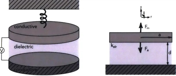
One compelling alternative to bulk piezo actuation is to incorporate ultrasound
transduction directly onto a silicon wafer chip where signal and image processing electronics could be placed very near the transducers themselves. This approach takes advantage of the many advancements in silicon fabrication that have come out of the Integrated Circuit (IC) and Microscale Electro-Mechanical Systems (MEMS) fields in the last three decades[26], [40]-[43]. Transducers of this type are called Micro-machined Ultrasound Transducers (MUTs) and they have been the focus of a considerable amount of research attention[8], [44]-[49]. There are two compelling approaches for generating and detecting the acoustic wave that both rely on microscale movable membranes, which can be electrically activated either capacitively across a small gap, or by including a piezoelectric material in the
membrane itself, shown in Figure 1.3. Microscale ultrasound transducers aim for improvements over traditional transducers in fabrication as well as device performance metrics such as coupling coefficient[50]-[52], bandwidth[49], [53], and image resolution[40],
conductive
support
movable membrane
U
piezo
Figure 1.3 Shows a schematic of a generic CMUT compared a generic PMUT. Both transducer types rely
on a movable membrane suspended above a gap (air or vacuum). In a CMUT the membrane moves when an electric field is applied between the bottom and top conductive electrodes. In a PMUT, a potential is applied across a thin film piezo material, inducing a strain in the membrane and causing it to move.
This electrostatic device is known as a Capacitive Micro-Machined Ultrasound Transducer, "CMUT." This actuation method uses an electrostatic force to move the
membrane. Here, a membrane is suspended across a gap (typically vacuum or sometimes air) and a voltage is applied to the membrane and the non-movable bottom electrode,
establishing an electric field across that gap. Because the two electrodes are oppositely charged, they experience an attractive force and the membrane moves towards the bottom electrode.
The other technique is known as the Piezo Micromachined Ultrasound Transducer,
"PMUT." This technique also relies on a suspended movable membrane. In these devices,
the membrane has an embedded piezo-material oriented such that an applied voltage induces an in-plane strain, causing the membrane to move out of its un-strained equilibrium plane.
Both CMUTs and PMUTs present significant advantages in manufacturing because they allow transducer to be fabricated directly onto a silicon wafer and easily integrated with the transmitting and receiving electronics. Locating the transducer next to the signal processing electronics has the potential to improve signal to noise ratio and therefore transducer sensitivity. One proposed strategy is to fabricate the integrated circuit and then fabricate the
MEMS device in a "MEMs-last" approach[57]. This approach minimizes the distance
between the signal processing electronics and the transducer, but results in temperature restrictions in the MEMS fabrication steps because high temperatures can damage the integrated circuits.
The dimensions of individual CMUT and PMUT cells vary widely depending on the design and intended application, and are typically in the 10-100s of microns range in diameter, with gap offsets of 10s of nm-a few microns. A single cell represents a single movable membrane. Because of the small size of these cells, often a single transducer element is comprised of many individual cells which are actuated in parallel, and an array
may consist of many elements which are in turn comprised of individual CMUT or PMUT cells.
Individual CMUT cells are generally larger than PMUT cells. The dimensions of
individual CMUTs are typically 100s of pim, thickness a few microns, with gap height of 100s of nm to a few microns. For example, one design of CMUTs for high frequency ultrasound ablation of tumors, the CMUTs had silicon membranes suspended over vacuum[58]. Dimensions were diameter 140 microns, thickness 6 microns, and gap of .4 microns.
Another design for in vivo imaging had rectangular membranes 80xl00microns, thickness of 500nm, and gap height 100nm, DC bias 80V with 35V amplitude signal[34].
The membrane material is a critical aspect of both CMUTs and PMUTs, and should be selected for device performance as well as fabrication methods. Dimensions and material properties dictate the acoustic behavior of the membrane. Many designs use silicon nitride[7], [59], [60] as the membrane material. Other membrane materials have also been explored, such as silicon-germanium[57], silicon, silicon dioxide[61], SU-8 [62], and diamond-like carbon[63]. Finite Element Analysis (FEA) simulations have shown that keeping dimensions constant but changing the material from silicon carbide to silicon dioxide change the transformer ratio by 2.4 times and the resonant frequency by 2.5 times, but did not change the bandwidth[61]. Therefore, membrane material should be carefully selected for the device application and the fabrication process.
Fabrication of suspended membranes is a challenge at the nanometer and micron length scale because the processes used in semiconductor fabrication generally rely on adding and subtracting layers. There are two strategies to achieve suspended membranes in
semiconductor fabrication. One approach is to use a sacrificial layer, where the sacrificial layer is laid down, the membrane is deposited on top, and then the sacrificial layer is dissolved or etched away. Examples include a photoresist sacrificial layer CMUT [57], an oxide sacrificial layer [52], [59], and a chrome sacrificial layer under a silicon nitride
membrane[40]. Typically, the sacrificial layer is chosen as a material that is easy to completely remove without damaging other structures on the wafer. A second fabrication strategy is to build the bottom electrode and dielectric offset layers on one wafer, build the top electrode and membrane on the other wafer, and then assemble the two halves together using wafer bonding[43], [64], [65]. The carrier wafer for the membrane can then be removed by
backside etching. These processes put limitations onto the materials and the fabrication. For example, a sacrificial layer requires an access hole (either on the front or backside) so that the etchant can reach the sacrificial layer and be removed. As a result, the air gap is not isolated from the surrounding environment without downstream processing. On the other hand, wafer bonding requires very smooth surface, vacuum, and high temperature in order to get strong adhesion between the two halves. The wafer bonding approach is potentially problematic for a "MEMS-last" device where the integrated circuit and transducer are located on one chip. Self-assembled suspended membranes with strong adhesion to their support layer have been demonstrated using fibrous biological materials such as collagen[66], but have not been demonstrated for semiconductor materials yet. One of the key challenges with additive processes and self-assembly of suspended membranes is strong adhesion between the membrane and the underlying support structure.
After fabricating the transducer elements, they must be incorporated into an ultrasound probe, so electronics packaging and acoustic interfacing is also an important design
consideration. When CMUTs were incorporated into probes for medical imaging, a silicone matching layer lens was cast into the front of the device, as well as a backing layer made
from silicone filled with metal oxide nanopowders[40]. The CMUT transducers were incorporated onto a rigid PCB[40] or flex circuit[8], [19] for packaging into a handheld probe. The processes involved in packaging these transducers into a probe must also be
considered in their design.
CMUTs and PMUTs have certain trade-offs relative to one another. The commercial areas where CMUTs and PMUTs will find each find their niche is not yet apparent, but there is enough evidence of relative advantages for each that there will be space for both.
CMUTs have received more research attention compared to PMUTs. CMUTs were originally proposed in in 1989[67] and are beginning to reach commercialization through Butterfly Network. CMUTs have a high bandwidth and as a result have higher imaging resolution compared to traditional bulk crystal transducers[8]. Unfortunately, they have high electrical impedance and therefore require high power compared to PMUTs. Further, acoustic power output is relatively low and as a result, CMUTs are limited in their ability to image deep tissues. The acoustic power is limited by the physics of operation, which are described in detail in Chapter 3. CMUTs typically require higher voltages for actuation, which can be on the order of 1OV[68], 130V[65], and 280V[7] for the peak voltage (AC magnitude + DC bias), and depend on the device design. The acoustic output of a CMUT is
limited by the volume displaced by the membrane, which is limited by the "pull in point" instability of capacitive transduction, described in detail in Chapter 2.
PMUT have received less attention, compared to their CMUT counterparts. One major
advantage of PMUTs compared to CMUTs is that they can be operated at lower voltages, and they have better penetration depth. The downside is smaller bandwidth. The fabrication of thin piezo films is a challenge relative to a metal electrode used in CMUTs, and a lot of work in the PMUT field has focused on fabrication of the transducer elements[50], [60], [69],
[70]. Furthermore, understanding the physics of actuation and therefore numerically
optimizing the design prior to fabrication has also been an area of active research[48], [71],
[72].
1.6 Thin film Acoustic Transducers
A few groups have developed thin film acoustic transducers using both piezo and
capacitive actuation. Capacitive actuation has the benefit of being nearly distortion-less in the acoustic regime (if properly designed) and therefore has been popular with audiophiles for a long time. In the home audio market, electrostatic speakers from companies such as Martin Logan are expensive but have exceptional sound quality due to the large bandwidth. Polymer
films, such as polyimide, have been used for the movable membrane material of air-coupled
capacitive acoustic transducers for decades[73]. More recently, miniaturized capacitive acoustic transducers have been fabricated and characterized in the audible frequency range[74]-[77].