Design and Prototype Fabrication of a Manipulator for
Semiconductor Test Equipment
by
Robert Ryan Vallance
B.S., Virginia Polytechnic Institute and State University (1994)
Submitted to the Department of Mechanical Engineering in partial fulfillment of the requirements for the degree of
Master of Science in Mechanical Engineering at the
MASSACHUSETTS INSTITUTE OF TECHNOLOGY
February 1996
© Massachusetts Institute of Technology 1996 All Rights Reserved.
Author
Robert Ryan Vallance Department of Mechanical Engineering January 19, 1996
Certified by - . .
Alexander H. Slocum Alex and Brit d'Arbeloff Associate Professor of Mechanical Engineering "sis Supervisor
Accepted by
_._
Ain A. Sonin Chairman, Departmental Committee on Graduate Studies ,,ASSA•,,-USE-TS-S "NST.i.TU. E
OF TECHNO)LOGY
JUN 26 1996
Eng.
Design and Prototype Fabrication of a Manipulator for
Semiconductor Test Equipment
by
Robert Ryan Vallance
Submitted to the Department of Mechanical Engineering on January 19, 1996 in partial fulfillment of the requirements for the
Degree of Master of Science in Mechancial Engineering
Abstract
This thesis describes a product development project that was part of the New Products Program in the Department of Mechanical Engineering at the Massachusetts Institute of Technology. The project focused on the development of the Universal Manipulator, an inexpensive, seven degree of freedom, pendant/manual controlled manipulator to position semiconductor test equipment. The Universal Manipulator was developed jointly with Teradyne, Inc., one of the world's leading manufacturers of semiconductor test equipment. Teradyne employees were responsible for the initial design specifications and subsequent design reviews. Graduate students within the Precision Engineering Research Group were responsible for the conceptual design, detailed design, and prototype fabrication. This thesis introduces why a new manipulator was needed, summarizes the project management, provides a thorough overview of the alpha prototype, and introduces the beta prototype.
Thesis Supervisor: Title:
Alexander H. Slocum
Alex and Brit d'Arbeloff Associate Professor Mechanical Engineering Department
Acknowledgments
Certainly, many people at Teradyne's STD and ICD divisions deserve much recognition, including Simon Longson, Carl Verdebre, and Dennis Legal. Special thanks to Art Lecolst for working so intently with us. We all owe much gratitude to Alex and Brit d'Arbeloff.
In addition, many people deserve credit for assisting us with the fabrication of the prototypes. Their insight was always useful and almost always correct. Thanks to Paul Preble and Bill Miskoe for dealing with illegible faxes and helping me escape from campus. Thanks to Dan Seger for giving us discounts. For the beta prototypes, I thank Glenn Cleaver, Kevin Uhlig, and Gerry for their effort in meeting a challenging deadline. I thank Frank Klaus, a German-trained toolmaker, for giving our bearings perfect fits.
I acknowledge Alex for his ceaseless creativity and enthusiasm, Rick for his management insight, the entire design team for late hours and hard work, and Debie for unloading the Kaydon bearings.
I thank God for being blessed with the capacity to question, learn, explore, and create. I thank my family for their loving thoughts and for forgiving me when I forget.
I thank Elizabeth for her compassion, encouragement, and devotion. I thank my friends and roommates for providing me with laughter.
I thank the design team: Carsten, Dave, Rolland, and Sep. I thank Alex for giving me the opportunity to design.
"Do not say that you're afraid to trust your mind because you know so little. Are you safer in surrendering to mystics and discarding the little that you know? Live and act within the limit of your knowledge and keep expanding it to the limit of your life. Accept the fact that you are not omniscient, but playing a zombie will not give you omniscience--that your mind is fallible, but becoming mindless will not make you infallible--that an error made on your own is safer than ten truths accepted on faith, because the first leaves you the means to correct it, but the second destroys your capacity to distinguish truth from error. In place of your dream of an omniscient automation, accept the fact that any knowledge man acquires is acquired by his own will and effort, and that that is his distinction in the universe, that is his nature, his morality, his glory."
Table of Contents
Design and Prototype Fabrication of a Manipulator for Semiconductor Test
Equipment 3 Abstract 3 Acknowledgments 5 Table of Contents 9 List of Figures 11 List of Tables 13
1. Introduction to the Thesis 15
1.1 The Semiconductor and Semiconductor Manufacturing Equipment Industries 16
1.1.1 Overview of Integrated Circuit Manufacturing 19
1.1.2 Ensuring Quality and Reliability in Integrated Circuits 22
1.2 Teradyne's Business and Products 24
1.3 The Semiconductor Test Equipment 26
1.3.1 Teradyne's Magnum Testhead and Cable Bundle 27
1.3.2 Testhead Manipulators 29
1.3.3 Probers and Handlers 32
1.4 Mechanical Issues in the Testing Process 34
1.5 Conceptual Solution to Teradyne's Mechanical Issues 36
1.6 Remaining Topics in Thesis 40
2. The Universal Manipulator Project 41
2.1 Overview and Principles of Concurrent Engineering 41
2.2 Implementing Concurrent Engineering 45
2.3 The Universal Manipulator Project 48
2.3.1 Organization of the Universal Manipulator Project 48
2.3.2 The Project Goals and Deliverables 50
2.3.3 The Project Schedule 51
2.3.4 The Design Team 54
2.3.5 The Design Tools 56
2.4 Discussion of the Universal Manipulator Project 61
2.4.1 The Design Process 61
2.4.2 The Design Team and Communication 64
2.4.3 Computer Aided Engineering System 65
2.4.4 Design for Manufacturability 67
2.4.5 Prototyping 68
2.5 Summary 69
3. The Design and Fabrication of the Alpha Prototype 71
3.1 The Design of the Alpha Prototype 71
3.1.1 The Base Subassembly 73
3.1.2 The Crossbase Subassembly 76
3.1.3 The Column Subassembly 82
3.1.4 The Twistarm Subassembly 90
3.1.5 The Cradle Subassembly 93
3.2 The Fabrication of the Alpha Prototype 97
3.3 The Assembly of the Alpha Prototype 99
3.4 Unresolved Design Issues 101
3.5 Summary 103
4. Conclusion 105
Appendix A: Universal Manipulator Specification 109
A. 1 Introduction 109
A.2 Design Specification 110
Appendix B: Project Schedules 127
B. 1 Introduction 127
B.2 Initial Project Schedule, Gantt Chart 128
B.3 Initial Project Schedule, PERT Chart 147
B.4 Beta Redesign Schedule, Gantt Chart 154
List of Figures
Figure 1.1: Flowchart of the Integrated Circuit Manufacturing Process 20 Figure 1.2: Uncut Silicon Wafer (Left) and Packaged Integrated Circuit (Right) 22
Figure 1.3: Failure Rate Model for Electrical Components 23
Figure 1.4: Teradyne Net Sales and Net Income Since 198516 25
Figure 1.5: Teradyne J971 Test System with RAM Manipulator 27
Figure 1.6: Illustration of STD's Magnum Testhead and Cable Bundle 28
Figure 1.7: ICD's Mainframe-Mounted Manipulator 31
Figure 1.8: The in2 Manipulator from inTEST Corporation 31
Figure 1.9: Hinged Manipulator from Electroglass 32
Figure 1.10: Photograph of a Floor Plan Arrangement with Two Probers 33
Figure 1.11: Photograph of a Typical Testhead/Prober Interface 34
Figure 1.12: Illustration of a Kinematic Coupling 38
Figure 1.13: Conceptual Solution to Teradyne's Mechanical Issues: A Kinematic
Coupling Interface and the Universal Manipulator 39
Figure 2.1: Illustration of Concurrent Engineering in Product Development 42 Figure 2.2: Illustration of Conventional Scheduling in Product Development 43 Figure 2.3: Organizational Structure of the Universal Manipulator Project 49
Figure 2.4: Approach Used for the Initial Project Schedule 53
Figure 2.5: Approach Used for the Beta Redesign Schedule 53
Figure 2.6: MIT Design Team During the Conceptual Design Phase 55
Figure 2.7: MIT Design Team During the Detail Design of the Alpha Manipulator 55 Figure 2.8: MIT Design Team During the Detail Design of the Beta Manipulator 55 Figure 2.9: Pro/Engineer CAD Software from Parametric Technologies 56 Figure 2.10: Microsoft Access Relational Database for Tracking Design Information_ 58 Figure 2.11: Multi-dimensional Design Space Described by Slocum14 62
Figure 3.1: The Alpha Prototype and Primary Subassemblies 72
Figure 3.2: Base and Crossbase Subassemblies in the Alpha Prototype 74
Figure 3.3: Kaydon MTO-145 Four-Point Contact Ball Bearing 75
Figure 3.5: Thomson Accuglide Size 25 Linear Ball Bearings, Dimensions and Load
Capacity 78
Figure 3.6: Thomson PPA Performance Pak Actuators 79
Figure 3.7: 23D204 Anaheim Automation Stepper Motor 80
Figure 3.8: 3/8 in. Ballscrew from Ball Screws and Actuators, Inc. 80 Figure 3.9: Dimension and Ratings for Lenze Model 14.436.04.2.0 Clutch Coupling _ 81 Figure 3.10: Drawing of Lenze Model 14.436.04.2.0 Clutch Coupling_ 82 Figure 3.11: Thomson Accuglide Size 45 Linear Ball Bearings, Dimensions and Load
Capacity Correspond to Figure 3.4 84
Figure 3.12: Conceptual Drawing of the Up/Down ACME Screw 85
Figure 3.13: Column Subassembly with the Telescoping ACME Screw Extended 86
Figure 3.14: Browning R206Q56-L Worm Gear Reducer 87
Figure 3.15: Photograph of Alpha Prototype with Telescoping Ballscrew 88
Figure 3.16: Photograph of the Bison 300 DC Gearmotor 89
Figure 3.17: Dimensions of the Bison 300 DC Gearmotor 89
Figure 3.18: Exploded View of the Twistarm Subassembly 91
Figure 3.19: Photograph of the Bodine 42A-GB PM DC Gearmotor 92
Figure 3.20: Dimensions of the Bodine 42A-GB PM DC Gearmotor 92
Figure 3.21: Cradle Subassembly 93
Figure 3.22: Illustration of a Typical Crossed Roller Linear Way 94
Figure 3.23: Drawing of the IKO CRW 6-300 Crossed Roller Linear Ways 95 Figure 3.24: Dimensions and Load Capacity of the IKO CRW 6-300 Crossed Roller
Linear Ways 95
Figure 3.25: Drive Assembly in Alpha Prototype's Left Cradle Arm 96
Figure 3.26: Torrington 6SF10 Plain Spherical Bearing 96
Figure 3.27: Photograph of the Assembled Alpha Prototype 100
Figure 3.28: Photograph of Alpha Prototype in Collision Position 102
List of Tables
Table 1: Initial Project Schedule, Milestones and Start Dates 52
Table 2: Beta Redesign Project Schedule, Milestones and Start Dates 52 Table 3: Primary Subassemblies in the Alpha Prototype of the Universal Manipulator 73
"The machine, the frozen form of a living intelligence is the power that expands the potential of your life by raising the productivity of your time."
Ayn Rand, Atlas Shrugged
1. Introduction to the Thesis
This thesis describes a product development project that was part of the New Products Program in the Department of Mechanical Engineering at the Massachusetts
Institute of Technology. The project focused on the development of the Universal Manipulator, an inexpensive, seven degree of freedom, pendant/manual controlled manipulator to position semiconductor test equipment. The Universal Manipulator was developed for Teradyne, Inc., one of the world's leading manufacturers of semiconductor test equipment. The project consisted of designing and fabricating an alpha prototype and subsequently designing and fabricating two beta prototypes. The thesis introduces why the Universal Manipulator was needed, describes how the project was managed, provides a thorough overview of the alpha prototype, and introduces the beta prototypes.
A small team of graduate students from the Precision Engineering Research Group (PERG), directed by Dr. Alexander H. Slocum, was responsible for the design and prototype fabrication. The Precision Engineering Research Group is a member of MIT's Laboratory for Manufacturing and Productivity (LMP). Teradyne employees were responsible for the initial design specifications and subsequent design reviews. After the beta prototypes were delivered, Teradyne was responsible for additional design modifications and preparing for production. The project required extensive effort from
other people including employees from Aesop, Inc. and several machine shops. The author has attempted to recognize all contributing individuals and companies.
Chapter 1 of the thesis introduces the Universal Manipulator project by beginning with the semiconductor and semiconductor equipment industries and narrowing to Teradyne's need for a new manipulator to position semiconductor test equipment. The semiconductor test process and the associated test equipment are introduced, and particular mechanical issues with the testing process and equipment are explained. The chapter concludes with a conceptual solution to Teradyne's mechanical issues, of which the new Universal Manipulator is a subset.
1.1 The Semiconductor and Semiconductor Manufacturing
Equipment Industries
The semiconductor industry has revolutionized the world with their ability to rapidly develop and apply new technology. For that reason, the boom of the semiconductor industry has been referred to as the second industrial revolution. As the world becomes dependent upon electronics, manufacturers of integrated circuits deliver increasingly powerful products with improved quality and reliability. To accomplish this, the industry continuously improves by developing new integrated circuits and by
improving manufacturing quality with new manufacturing equipment and processes.
The history of the semiconductor industry tells the story of international competition between Europe, the United States, and Japan. Malerba describes why the Europeans lost their semiconductor industry to the United States (U.S.) when the U.S.
invested extensively in defense related technologies'. More familiar to Americans, however, is the loss of our semiconductor industry to Japanese manufacturers during the
1980s. Angel explains how the U.S. market share in the semiconductor industry shrunk from 58% to 37% while Japan's grew from 26% to 49%2. Angel attributes the loss in market share to many factors, but chiefly problems with "low yields"3 and problems with
matching market demand and production capabilities. Semiconductor manufacturing facilities in the U.S. were designed for large production rates, and as a result it was difficult to produce quality products when demand was low.
In addition to low yields and production problems, Angel also attributes the Japanese market take-over to Japan's effective long-term relationships with their equipment suppliers. U.S. manufacturers elected to not form long term relationships because they preferred to selectively jump from supplier to supplier depending on which had the best technology at the moment. In addition, U.S. manufacturers often forwarded some of the cost of their fluctuating market demand to their equipment suppliers in the form of canceled or reduced orders on new manufacturing equipment. In contrast, the Japanese formed strong relationships with equipment suppliers, sponsoring investments in new technologies and strengthening the Japanese semiconductor equipment industry. In 1990, the Tokyo Business Today published that between 1983 and 1989 the U.S.
1 Malerba, Franco. The Semiconductor Business. Frances Pinter Publishers. London. 1985.
2 Angel, David P. Restructuring for Innovation, The Remaking of the U.S. Semiconductor Industry. The
Guilford Press. New York, New York. 1994.
3 The term "low yields" is used to indicate that the percentage of acceptable dies or chips is a small
market share of semiconductor equipment had dwindled from 62% to 41% while the Japanese share had increased from 28% to 48%2.
Many economic forecasters predicted the loss of the semiconductor industry to Japan, but instead, U.S. manufacturers revitalized by structuring themselves for innovation2 and applying Total Quality Management (TQM) techniques4. In 1994, the
U.S. semiconductor industry lead the $101.88 billion worldwide semiconductor market
with a 32.9% market share compared to Japan's 28.9% market share5,6. To accomplish
this dramatic reversal, U.S. manufacturers focused their attention on production and quality issues, including relationships with their equipment suppliers.
The semiconductor industry's rapid pace of technological innovation significantly impacted the semiconductor equipment manufacturers. To maintain the pace of semiconductor manufacturers, equipment suppliers were forced to be fast and innovative. The short product life cycles were beneficial, however, because semiconductor manufacturers regularly invested in new equipment to produce their latest integrated circuits.
4 Shiba, Shoji, Alan Graham, and David Walden. A New American TQM, Four Practical Revolutions in
Management. Productivity Press and the Center for Quality Management. Portland, Oregon and Cambridge, Massachusetts. 1993.
5 Bulkley, Ann E. "Strong Chip Sales Spark Capital Equipment Investment". Economic Indicator Column.
Semiconductor International. August, 1995.
6 W. Europe and Korea/ROW were close behind with 19.4% and 18.8%, respectively.
1.1.1 Overview of Integrated Circuit Manufacturing
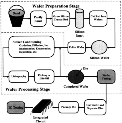
The details of the semiconductor manufacturing process are described in several sourceS7,8,9. The general process is condensed and illustrated by the flow chart in Figure
1.1. The manufacturing process begins with silica sand and ends with an integrated circuit. The first phase of processing is wafer preparation. Silica sand, which contains about 1% impurities, is refined through chemical reactions to obtain ultrapure polycrystalline silicon. The polycrystalline silicon is melted and recrystallized (often referred to as "growing") into a rod of single-crystal silicon using either the Czochralski or float zone techniques. The silicon crystal rod is ground round to an 8" diameter, and the rotational orientation of the crystal is determined. Then the crystal rod is sliced into thin wafers1o. Each wafer receives a mirror-like finish by polishing the wafer to the proper surface quality.
The next phase in the manufacturing process, wafer processing, generates a rectangular array of "dies" on the surface of the wafer. Each die is an intricate topographical structure of device regions, interconnections, and pads which will become the heart of an integrated circuit. In Figure 1.1, the wafer processing stage is broken into
7 Gise, Peter E. and Richard Blanchard. Semiconductor and Integrated Circuit Fabrication Techniques. Reston Publishing Company, Inc.. Reston, Virginia. 1979. MIT Library: TK7871.85.G49 (1979)
8 Wolf, S. and Tauber, R. Silicon Processing for the VLSI Era Volume 1: Process Technology. Lattice
Press. Sunset Beach, CA. 1986.
9 Wolf, S. and Tauber, R. Silicon Processing for the VLSI Era, Volume 2: Manufacturing Technology. Lattice Press. Sunset Beach, CA. 1986.
10 Currently, wafers are 200 millimeters in diameter and about .7 millimeters thick. The industry is
beginning to switch to a new standard diameter of 300 millimeters, but this will take several years to complete.
three iterative steps: surface conditioning, photolithography, and etching or lift-off. With each iteration, a layer of patterned material is built-up on the surface of the die until the topography is complete.
W---afer Prearation Sta--e
S~I S~I S~I S~I S~I I- I S~I S~I S~I S~I S~I S~I S~I S~I S~I S~I S~I S---I S~I I.' Integrated Circuit
Figure 1.1: Flowchart of the Integrated Circuit Manufacturing Process1'
The most common surface conditioning processes are diffusion, ion implantation,
thermal oxidation, vapor deposition, and cleaning. Diffusion uses concentration gradients
at high temperatures to form the p-n junctions by introducing impurities or dopants in gas,
liquid, or solid form into the silicon. Ion implantation, another method of introducing
1"
This figure was adapted from a figure in Chapter 1 of Silicon Processing for the VLSI Era Volume 1:Process Technology by Wolf and Tauber, Lattic Press, 1986.
20 I I I, I I I I
dopants, is becoming increasingly more common because of its superiority over the diffusion process. Thermal oxidation is the process of generating a protective coat of silicon oxide (SiO2) on the surface of the die. Vapor deposition is a process for applying
a thin film (.5 - 20 gm) of varying materials onto the die.
After surface conditioning is complete, the die is subjected to photolithography. The first step in photolithography is coating the wafer with a thin film of photoresist. Radiation in the form of ultraviolet light, electrons, or x-rays is applied to the photoresist through a mask with a pattern of opaque and transparent areas. In the subsequent developing process, the areas exposed to the radiation are generally made soluble in a specific solvent. Following development, the exposed regions can then be removed with etching12. The entire process replicates the pattern of the mask on the surface of the dies. The iterative loop of surface conditioning, photolithography and etching continues until the topography on the die's surface is complete.
After the wafer processing stage, each die on the wafer is tested. The wafer is then cut into individual dies, and the dies which passed the tests are generally encapsulated within a black ceramic package. After packaging, each integrated circuit is usually tested a final time prior to shipping.
12 Lithography can also be used with a process known as "lift-off' to add material to the die. 21
Figure 1.2: Uncut Silicon Wafer (Left) and Packaged Integrated Circuit (Right)
1.1.2 Ensuring Quality and Reliability in Integrated Circuits
In today's world, almost everything is dependent upon the performance of integrated circuits. They are used in nearly every electronic device, and they are becoming increasingly popular in mechanical systems as controllers. Integrated circuits are commonly used with little regard for their inherent reliability and quality of performance. How is it that integrated circuits appear to operate continuously without failing? This phenomenon is the result of the failure rate characteristics of electrical devices and effective testing during the manufacturing process.
Figure 1.3 illustrates a common model of the failure rate (probability of failure) of electronic devices as a function of time when operated under design conditions (temperature, voltage, and current). Electronic devices exhibit a high probability of failure near the beginning of their life (commonly referred to as "infant mortality"), but the failure rate eventually reaches a low and nearly constant value. This failure rate
model is much different than the degradation exhibited by mechanical components in which the failure rate continually increases with time. Once an electrical device has passed the infant mortality stage, it generally operates indefinitely with a low probability of failure 3.
Hazard Rate Dead on arrival (DOA) failures which tested OK but were later discovered as
X(t) non-functional because of an event-dependent situation such as handling
nitm which made them fall Defore the use clock started.
ing failure which occurred during early operation of
It failure rate is time dependent and described by the
t mortality model.
Steady-state failure rate from random events described
by the exponential failure modeL
No Operating Time
Infant
j
Steady-StateMortality 04 hours Operation
-1 year +
Figure 1.3: Failure Rate Model for Electrical Components14
The second reason for the quality and reliability of integrated circuits is effective testing during the manufacturing process and the testing of the device prior to shipment. Semiconductors are typically tested at two periods in the manufacturing process as shown in Figure 1.1. Semiconductor manufacturers have discovered that there is a significant economic advantage for testing dies prior to cutting the silicon wafer and packaging because money is not wasted on packaging defective dies. Another set of tests are
13 Electrical devices are often accelerated through the infant mortality phase with a process known as "burn-in" in which the device is subjected to high operating temperatures.
14 Barringer, Paul. "Reliability Engineering Principles". Barringer & Associates. Humble, Texas. 1994. 23
performed on the integrated circuit after they have been packaged and prior to shipment. These tests insure that the devices are functional and beyond their infant mortality stage. Together, the failure rate characteristics described above and effective testing during production, nearly eliminate all defective integrated circuits and insure reliable electronic devices.
1.2 Teradyne's Business and Products
In the late 1950s, Nick DeWolf observed a need in the semiconductor industry for a device capable of testing diodes during production. In 1960, DeWolf joined with Alex d'Arbeloff'5 and formed Teradyne, Inc. in Boston Massachusetts to fulfill this market
need. Teradyne went public in 1970, and has been traded on the New York Stock Exchange since 1979. Today, Teradyne describes their business as "the creative application of systems technology to practical problems in the design, manufacture, and servicing of electronics" 16. Teradyne's products include test systems for semiconductors,
test systems for circuit-boards, test systems for telecommunications, and backplane connection systems. Teradyne designs, manufactures, sales, and services these systems throughout the United States, Europe, and Asia's Pacific Rim.
Teradyne's semiconductor test systems are designed by two separate divisions, the Industrial/Consumer Division (ICD) in Boston, Massachusetts, and the Semiconductor
15 Alex d'Arbeloff remains in the company as Chairman of the Board and President. Nick DeWolf is no longer associated with the company.
Test Division (STD) in Agoura Hills, California. ICD is responsible for test systems related to linear and mixed-signal integrated circuits, and STD is responsible for test systems related to VLSI and memory integrated circuits. Teradyne's customers use the test systems to increase product performance, improve product quality, shorten time to market, enhance manufacturability, conserve labor costs, and increase production yields. Prices for Teradyne's test systems range from less than $100,000 to $5 million or more7.
600 S500 400 300 200 100 0 70 60 50 = 40 S 30 20 10 0 -10 Z -20 -30
Net Sales $M -4--Net Income
Figure 1.4: Teradyne Net Sales and Net Income Since 198516
Teradyne managed to survive the hard times experienced by U.S. semiconductor equipment manufacturers during the 1980s. Through the leadership of d'Arbeloff and other managers, Teradyne initiated Total Quality Management (TQM) techniques in 1990. Since that time, Teradyne has experienced four straight years of increased sales as shown in Figure 1.4, including a record year in 1994. Semiconductor manufacturers
17 Teradyne's 10-K SEC filing contained in Teradyne's 1994 Annual Report to Shareholders. 25
spent two years increasing their production capacity and suddenly discovered a lack of test capacity. Record sales were recorded by Teradyne during 1994's fourth quarter in all of their products, including VLSI logic, memory, and linear/mixed-signal'6.
The highly technical nature of Teradyne's products requires a large engineering and development effort'8. Teradyne's engineering and development expenditures for new and improved products were approximately $62.0 million in 1992, $62.4 million in 1993, and $70.4 million in 1994. These recent engineering expenditures resulted in the release of four new test systems with more to arrive in early 199617,'19.
1.3 The Semiconductor Test Equipment
Teradyne's test systems typically contain four pieces of equipment: a testhead, a mainframe computer, a workstation computer controller, and a manipulator. Figure 1.5 shows a photograph of Teradyne's J971 VLSI Test System. The testhead is packed with circuit boards which are responsible for the initial analog signal processing when a die is tested. The results of the testhead's signal processing are then forwarded to the mainframe for further processing as digital signals. A large cable bundle contains the power cables and the intermediate signals wires.
18 Traditionally, these expenditures have focused on electrical engineering issues, but recently an increased share has been invested in solving mechanical problems that are addressed in Section 1.4 of this chapter.
19 STD introduced three new test systems in 1994, one new system to the J971 product line, and two new
systems to the J921 product line. In 1995, ICD released the A565 test system. Both ICD and STD are expected to release new product lines in early 1996.
Figure 1.5: Teradyne J971 Test System with RAM
Manipulator
1.3.1 Teradyne's Magnum Testhead and Cable
Bundle
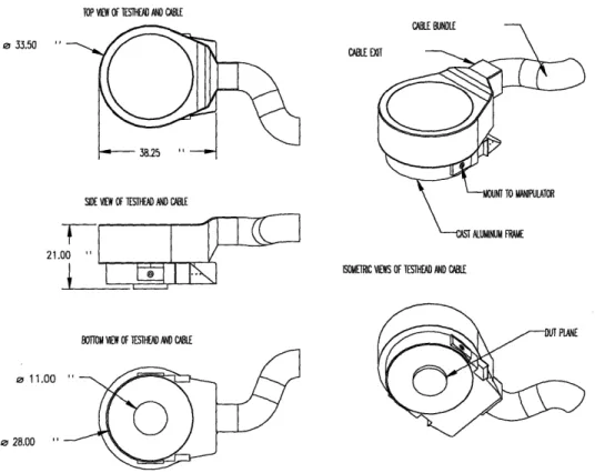
Teradyne's STD and ICD divisions sale about nine different test systems which are available in a variety of testhead, mainframe, and cable configurations. The new Universal Manipulator was initially designed to be used with STD's Magnum testhead, illustrated in Figure 1.6. It is anticipated that the Universal Manipulator will later be adapted for use with Teradyne's other testheads.
TOP MIE OF TESTEA AND CABLE
SIDE MEW OF TESTHEAD AND CABLE
21.00
ISOMETRIC MEWS OF TESIHEAD AND CABLE
BOTTOM ViEW OF TESTHEAD AND CABLE
0 11.00
0 28.00
Figure 1.6: Illustration of STD's Magnum Testhead and Cable Bundle
The Magnum testhead, STD's newest testhead, weighs approximately 900 pounds, is 83.8 cm (33 in.) in diameter and 53.3 cm (21 in.) tall. The structure of the testhead is provided by an aluminum casting. The cable bundle used with the Magnum testhead weighs approximately 1560 N (350 lbs), has a cross-sectional area of about 323 cm2 (50 in.2), and is about 2.29 m (7.5 ft.) long20. The circuit boards within the testhead
are cooled by coolant water supplied from the mainframe through flexible hoses included within the Magnum's cable bundle.
20 The cable bundle for the Magnum testhead played a significant role in the specifications of the Universal Manipulator because it subjected the testhead and manipulator to large external forces and torques.
28
S33.50
1.3.2 Testhead Manipulators
Teradyne's testheads are supported by manipulators which position and orient the testhead relative to probers or handlers. Probers and handlers are described in Section 1.3.3. Four types of manipulators were common prior to the development of the Universal Manipulator:
1. the RAM manipulator, sold by Teradyne's' ICD and STD divisions, 2. mainframe-mounted manipulators, sold by Teradyne's ICD division, 3. the in2 manipulator, sold by inTEST, and
4. a hinged manipulator, sold by Electroglass.
Traditionally, manipulators moved the testhead with assistance from a person pushing or pulling the testhead, by driving the testhead with motors controlled by a hand-held pendant, or by a combination of the two methods.
Both STD and ICD commonly sold the RAM manipulator, shown in the Figure 1.5, with their test systems. The RAM manipulator used human power and a motor to move the testhead with seven degrees of freedom21:
1. Swing positioning about the manipulator column, 2. Up/down positioning in the vertical direction, 3. In/out positioning in the x-direction,
4. Side-to-side positioning in the y-direction,
5. Twist rotation about the x-axis,
6. Tumble rotation about the y-axis, and
21 The testhead has seven degrees of freedom, three position, three orientation, and a redundant degree of freedom provided by the swing motion. Swing is often used by operators to move the testhead to the service position.
7. Theta rotation about the z-axis.
The only powered motion on the RAM manipulator was the twist rotation about the x-axis. All of the remaining motions were powered by a human operator pushing or pulling on the testhead. Counterweights balanced the weight of the testhead so that a human could lift or lower the testhead by hand to accomplish up/down positioning in the vertical direction. The testhead cable was held by a cable support on the manipulator's vertical column and a gas spring behind the column.
In addition to the RAM manipulator, ICD sold a manipulator that attached to the mainframe computer and was supported by the mainframe computer's structure. This style of manipulator is shown in Figure 1.7. The mainframe-mounted manipulator provided motions similar to the RAM manipulator.
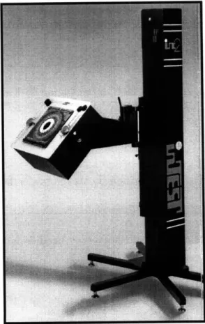
Other companies sold third-party manipulators as alternatives to Teradyne's manipulators. Two of the leading competitors were the in2 manipulator from inTEST
Corporation shown in Figure 1.8 and the simple one degree-of-freedom, hinged manipulator sold by Electroglass which is shown in Figure 1.9.
Figure 1.7: ICD's Mainframe-Mounted Manipulator
Figure 1.9: Hinged Manipulator from Electroglass
1.3.3 Probers and Handlers
Teradyne's test equipment is used in production with either a prober or a handler. A prober positions an uncut silicon wafer beneath a testhead, and a handler positions a
packaged IC beneath a testhead. Probers and handlers are stationary machines which internally move the wafer or IC. A hole in the prober or handler allows the testhead electronics to be connected to the silicon wafer or IC. The process of positioning and orienting the testhead relative to the prober or handler is commonly referred to as "docking" the testhead. The wafer or IC being tested is called the Device Under Test (DUT), and the plane where the testing occurs is called the DUT plane.
Probers are generally capable of positioning and orienting a wafer with three position degrees of freedom and a rotation degree of freedom for alignment. Probers and
handlers are manufactured by different equipment suppliers, and as a result, almost every prober or handler has a unique design. Some probers and handlers position the wafer or IC horizontally facing upwards toward the ceiling. Other probers and handlers position the wafer or IC horizontally but facing downward towards the floor. Still others position the wafer or IC so that it is vertically oriented or at a 550 angle to the floor. Figure 1.10
shows a photograph of a dual setup with two probers.
Figure 1.10: Photograph of a Floor Plan Arrangement with Two Probers
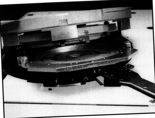
The electrical connections between the testhead electronics and the die or IC being tested within the prober or handler is made by the testhead interface. A typical interface is illustrated in Figure 1.11. Alagheband22 described the components within the interface
and their role in the docking of testheads to probers and handlers.
22 Alagheband, A. "Teradyne: A Kinematic Interface for Semiconductor Test Equipment". A case study published by MIT's Laboratory for Manufacturing and Productivity. 1995.
Figure 1.11: Photograph of a Typical Testhead/Prober Interface
1.4 Mechanical Issues in the
Testing Process
Alex d'Arbeloff, Chief Executive Officer of Teradyne, described
the history of the
integrated circuit testing process with the following analogy:
If you drop a frog into a pot of boiling water, it will immediately jump out, but if you drop it in cool water and gradually
turn up the heat it will remain.22
When semiconductors and integrated circuits were first
produced, tests were
performed by technicians using probe needles to measure voltages
and current. From this
history, the semiconductor industry became trapped into moving
the test equipment to the
DUT rather than moving the DUT to the test equipment.
Moving the test equipment was
not a problem twenty years ago, but this is no longer true.
As integrated circuits become
more powerful, they require more complex testing equipment.
The test equipment must
be faster and more accurate than the devices being tested,
yet be made with existing 34
technology. As a result, test systems are enormous with huge testheads and cable bundles. This size problem compounds with the variety of probers and handlers available and their respective floor plan arrangements. It is ironic that as the devices being tested became more complex, they became smaller, but the test equipment became larger and heavier.
As the size and weight of test equipment increased, mechanical issues in the test process became evident which had been neglected for many years. One issue encountered was the size of the manipulator required to lift and move the large testheads. The load capacity of the RAM manipulator became a serious issue when Teradyne's STD division began to design the Magnum testhead which is described in Section 1.3.1. It was determined that the RAM manipulator was not strong enough to handle the Magnum testhead. The large cable bundles were also becoming an issue because the external forces applied to the testhead and manipulator pulled the testhead and created linear forces and rotational torques. In addition the wires in the cable bundle became damaged due to the tension forces in the cable as the bundle flexed while the testhead was moved.
Problems with repeatability and accuracy were also becoming issues, because the number pads that the probe needles had to touch were increasing while the size of the pads and distance between neighboring pads decreased. As a result, the testhead needed to be positioned and oriented relative to the prober or handler with greater accuracy. Repeatability was necessary because users wanted the testhead to repeatedly go to the
same location after moving the testhead and servicing the interface.
~UIIP~-~-·I~·--·lllar`·---·-r"l~----Another mechanical issue was that as the probe needles contacted the pads, they often scraped and damaged the surface of the die. Scraping occurred because the motion of the testhead was not perpendicular to the pads during the docking process.
All of these mechanical issues were causing significant increases in the time to dock a testhead to a prober or handler and reducing the quality of the testing process. Semiconductor manufacturers were quickly becoming frustrated with test equipment performance. Teradyne's management also realized that these issues would only become worse as integrated circuits continued to become faster and more powerful.
In summary, Teradyne needed to resolve the following issues to improve the quality of the testing process, reduce the docking time, and satisfy their customers:
1. a stronger manipulator to support future testheads and cable bundles, 2. an improved method for supporting the cable bundle,
3. reduce the bending and flexing of the wires inside the cable bundle, 4. increase the accuracy in the docking process,
5. increase the repeatability between docking processes, 6. increase manipulator manufacturability,
7. ensure that the final travel of the interface needles is normal to the die surface, and
8. a single manipulator that could be used with all probers and handlers by Teradyne's STD and ICD divisions.
1.5 Conceptual Solution to Teradyne's Mechanical Issues
In response to Teradyne's mechanical issues, Dr. Alexander H. Slocum, Associate Professor of Mechanical Engineering at MIT and the Director of the Precision
Engineering Research Group (PERG), proposed a solution to Alex d'Arbeloff: design a new manipulator and design a new testhead interface based on a kinematic coupling.
Kinematic couplings have been used for years in the precision engineering community for repeatably positioning and orienting two objects relative to each other. Methods for designing kinematic couplings were provided by Slocum23,24,25, and Slocum
and Donmez26 demonstrated that kinematic couplings can have repeatability on the order
of 0.3 tgm in the machine tool industry. More recently, Van Doren's doctoral thesis27
described the use of kinematic couplings in the semiconductor equipment manufacturing industry with a specific application to wafer handling robots for lithography. Teradyne's new kinematic coupling interface was designed by Michael Chiu, a doctoral student in the Precision Engineering Research Group, and described by Alagheband2.
The kinematic coupling solution, conceptually illustrated in Figure 1.12, uses three grooves mounted on the prober or handler and three balls mounted on the testhead. When the testhead is docked, the three testhead balls rest in the three grooves mounted on the prober or handler such that contact occurs at only six points, two points between each
23 Slocum, A. "Kinematic Couplings for Precision Fixturing -Part I: Formulation of Design Parameters".
Precision Engineering: Journal of the ASPE. Vol. 10, No. 2, April 1988, pp. 85-91. 24 Slocum, A. Precision Machine Design, Prentice Hall, 1992.
25 Slocum, A. "Design of Three-Groove Kinematic Couplings". Precision Engineering: Journal of the
ASPE. Jan. 1992.
26 Slocum, A and Donmez, M. "Kinematic Couplings for Precision Fixturing - Part II: Experimental Determination of Repeatability and Stiffness". Precision Engineering: Journal of the ASPE. Vol. 10, No. 3, July 1988, pp. 115-122.
ball and groove. Thus, the kinematic coupling repeatably and accurately constrains all six degrees of freedom of the testhead relative to the prober or handler.
Figure 1.12: Illustration of a Kinematic Coupling
Kinematic couplings normally depend upon the gravitational force to pull the coupling's balls into the grooves. Unfortunately, testheads are often docked to probers and handlers in orientations where the gravitational force may not be capable of pulling the balls into the grooves. Thus, Chiu's interface design depends upon an actuated coupling capable of pulling the balls into the grooves. To minimize the actuation force needed in the interface coupling, it was specified that the Universal Manipulator should be capable of supporting the testhead in a compliance mode. The compliance mode
27 Van Doren, M Precision Machine Design for the Semiconductor Equipment Manufacturing Industry. Ph.D. Thesis. Massachusetts Institute of Technology. 1995.
would allow the testhead to be moved within a limited range with an actuation force of less than 155 N (35 lbs).
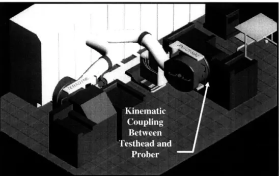
The solution proposed by Slocum resolves the mechanical issues described in Section 1.4. The new manipulator would be designed to handle larger and heavier testheads, it would be operable with all of the probers and handlers in each floor plan arrangement, and it would be inexpensive. The new kinematic coupling interface would increase accuracy and repeatability. The kinematic interface would also reduce die scrubbing by insuring that the last 760 gim (.030 in) of travel was normal to the die. Figure 1.13 illustrates the conceptual solution of a new manipulator combined with a kinematic coupling.
Figure 1.13: Conceptual Solution to Teradyne's Mechanical Issues: A Kinematic Coupling Interface and the Universal Manipulator
1.6 Remaining Topics in Thesis
This thesis describes the development of Teradyne's new Universal Manipulator, the manipulator designed in response to Slocum's conceptual solution to Teradyne's mechanical issues. The project began in the spring of 1994 and should culminate with the market release of the manipulator during 1996. The thesis reflects on the management of the project as well as describing some of the design and manufacturing details.
Chapter 2 describes the Universal Manipulator project in terms of concurrent engineering and conventional product development management. Attention is given to the how the joint project between Teradyne and MIT was planned, structured, and
scheduled.
Chapter 3 describes the design of the Universal Manipulator at the alpha prototype stage, and then describes the manufacture and assembly of the alpha prototype. This chapter also summarizes the design issues that remained unresolved at the completion of the alpha prototype.
Chapter 4 concludes the thesis by summarizing the accomplishments of the Universal Manipulator project and the anticipated success of the Universal Manipulator and kinematic coupling interface in the marketplace.
2. The Universal Manipulator Project
The design of the Universal Manipulator was intended to be a concurrent engineering project in which the designers worked closely with Teradyne and the manipulator manufacturer. This chapter describes the Universal Manipulator project in light of concurrent engineering, and attempts to summarize the benefits that were experienced due to the increased integration.
Chapter 2 begins with an overview of concurrent engineering, focusing on the principles and modem tools for implementation. The following sections present the details of the Universal Manipulator project in terms of the design team, resources, schedule, budget, and deliverables. A subsequent discussion focuses on how the project was effectively concurrent and how the project concurrency could have been improved.
2.1 Overview and Principles of Concurrent Engineering
Product development is a complex process involving many disciplines such as industrial design, design engineering, manufacturing engineering, marketing, and sales. Over recent years, extensive effort was invested to determine how companies can develop higher quality products faster and cheaper. Overwhelmingly, academia and industry pointed to concurrent engineering as one solution.
Concurrent engineering (CE) describes a design process in which all aspects of the product life cycle, from product conception to product disposal, are considered
simultaneously. Figure 2.1 illustrates how the marketing, design, manufacturing, and sales disciplines might be scheduled within a CE project. The arrows in the illustration represent information flow between the disciplines. For instance, marketing might develop new product ideas and then forward them to design engineering. Design engineering would then develop design concepts and forward them back to marketing for customer review and to manufacturing for production review. While marketing and manufacturing review the designs, the design engineering continually progresses. Every discipline is attempting to work in parallel with the most recent design information. It is important to observe that the scheduled activities generally overlap and that information is transferred often and iteratively.
Marketing
Design Engineering
Manufacturing Engineering
Sales
Time
Figure 2.1: Illustration of Concurrent Engineering in Product Development
Concurrent engineering is dramatically different than the conventional design process in which information is transferred between disciplines sequentially as illustrated in Figure 2.2. This sequential information transfer is often referred to as "over-the-wall" because there is typically very little integration, and the information receivers are generally left to resolve any problems. Concurrent engineering is beneficial because most
of the costs associated with a product are defined during the early design stages. It becomes increasingly expensive to make design changes as the product progresses from design towards production.
Time
Figure 2.2: Illustration of Conventional Scheduling in Product Development
Several books have been published that focus on the product development process and concurrent engineering. Ulrich and Eppinger' published a thorough book on the product development process. Nevins and Whitney2 wrote a book which addresses the
concurrent design of the product and the product's production process. Clausing published a book on total quality development3, and Phadke has published a book on
designing products that are robust to changes in design and manufacturing4. In addition,
many books exist on general management of engineering design projects5 '6'7. These
1 Ulrich, K.T. and S.D. Eppinger. Product Design and Development. McGraw-Hill, Inc. New York.
1995.
2 Nevins, J.L., and D.L. Whitney. Concurrent Design of Products and Processes. McGraw-Hill. New
York. 1989.
3 Clausing, Don. Total Quality Development. ASME Press. 1994.
4 Phadke, Madhav S. Quality Engineering Using Robust Design. Prentice-Hall. Englewood Cliffs, New Jersey. 1989.
5 Hales, Crispin. Managing Engineering Design. Co-published by Longman Scientific & Technical in England and John Wiley & Sons in the United States. 1993.
6 Bronikowski, Raymond. J. Managing the Engineering Design Function. Van Nostrand Reinhold
Company. New York, New York. 1986.
general books focus on fundamentals such as selecting financially sound projects, defining project objectives, scheduling projects, organizational issues, project
supervision, and the design process.
Concurrent engineering has received extensive attention in industrial and academic research publications. In the United States, the Department of Defense (DoD) and the Defense Advanced Research Projects Agency (DARPA) have funded extensive concurrent engineering research in academia. The DARPA Initiative on Concurrent Engineering (DICE) was initiated in 1988 to encourage concurrent engineering in the US military and industrial base. Many large companies such as Hewlett-Packard, Motorola, AT&T, Texas Instruments, Chrysler, and IBM have all recognized the advantages of concurrent engineering8. Research publications on concurrent engineering have
addressed topics such as:
1. effective scheduling of project tasks, 2. product data modeling,
3. information systems and databases,
4. computer-aided engineering (CAE) systems,
5. cost estimation and cost models, and
6. design team communication and interaction.
7 Cross, Nigel. Engineering Design Methods: Strategies for Product Design. John Wiley & Sons. New York, New York. 1994.
8 Jo, Hyeon H., Hamid R. Parsaei, and William G. Sullivan. "Principles of Concurrent Engineering".
Concurrent Engineering, Contemporary Issues and Modern Design Tools. Chapman & Hall. New York.
2.2
Implementing Concurrent Engineering
The goal of considering the entire product life cycle during the design stage is a difficult task. To help accomplish this goal, industry and academia have developed many tools for performing concurrent engineering. The primary tools can be grouped into five categories:
1. multi-disciplinary teams, 2. design for 'X' philosophies,
3. computer aided engineering (CAE) systems, 4. information management systems, and
5. product cost estimation.
The most successful tool in concurrent engineering is probably the multi-disciplinary design team. When large companies implement concurrent engineering, a product development team is formed that generally consists of members that represent each of the product's life-cycle issues. For instance, a team might be formed that consists of design engineers, manufacturing engineers, quality control, marketing, sales, and maintenance. The team is often responsible for the entire product development process, beginning with determining the customer's needs and continuing through to production. The experience and knowledge base of a multi-disciplinary team helps companies develop products that are more likely to meet customer needs, have exceptional quality, and are less expensive to manufacture.
The design for 'X' philosophies in which 'X' may stand for manufacturability, assembly, reliability, recyclability, disassembly, etc. are common to nearly every concurrent engineering effort. These philosophies help designers focus attention on the
wide variety of life-cycle issues. Common tools for implementing DFX philosophies include multi-disciplinary teams, general rule-based approaches that are applicable to a broad range of design problems, and expert systems that address a narrow range of design problems. A common rule-based approach is the Boothroyd-Dewhurst Design for Assembly process9'10,11.
An essential ingredient in concurrent engineering is the computer-aided engineering (CAE) system. A computer aided design (CAD) system is the pillar of any CAE system. The capabilities of modern CAD vary greatly. Simple and inexpensive CAD systems help designers create two-dimensional drawings of parts. More complex and expensive CAD systems allow designers to create "virtual" prototypes of the entire product. Virtual prototypes are created by forming three-dimensional solid models of the product's components and then assembling them together to form the entire product. The solid models and virtual prototypes can be used for analysis and manufacturing as well as generating drawings.
The CAD software industry has provided an extensive range of software for analyzing the CAD system solid models and virtual prototypes. For instance, a designer can perform a kinematic analysis to determine position, velocity, acceleration, and forces on dynamic assemblies or use finite element analysis (FEA) software to determine the
9 Boothroyd, D. Design for Assembly Handbook. Boothroyd Dewhurst, Wakefield, RI. 1985.
10 Boothroyd, G. and P. Dewhurst. Product Design for Assembly. Boothroyd Dewhurst, Inc. Wakefield,
stresses, strains, deflections, modes, and natural frequencies within a part subjected to complex loading.
Information management becomes an increasingly difficult task as the design process becomes more concurrent because information is transferred more often. To help manage the information burden, several systems now include database software with their CAD systems. These databases help track revisions to solid models and drawing
changes.
CAD systems are also being integrated with more advanced data systems called
document management (DM) or product data management (PDM). DM and PDM software packages help companies control information and workflow by integrating data from the design, production, and service support. PDM software helps integrate distributed data sources within companies. PDM aims to give access to the company's product data to many users simultaneously'2,13.
Another class of useful tools are cost estimation methods. With these methods, designers begin estimating the cost of the product early in the design stages and refine the estimate as the product progresses towards production. This allows designers to include the effects on product cost when comparing design alternatives. Cost estimation is a difficult task, however, because it is often difficult to acquire accurate cost estimates for
n Boothroyd, G. and P. Dewhurst. "Product Design for Manufacture and Assembly". Design for
Manufacture: Strategies, Principles, and Techniques. Addison-Wesley Publishing Company. 1991.
12 "Engineering Drives Document Management". Machine Design. June 15, 1995. p. 77-78.
47
custom parts. For cost estimation to be effective, designers must be well integrated with the product manufacturer(s).
2.3 The Universal Manipulator Project
The Universal Manipulator project was performed jointly between Teradyne, Inc. and a design team from the Precision Engineering Research Group at MIT's Laboratory for Manufacturing and Productivity. The project was part of the New Products Program which aims to train students in product development by designing and prototyping real products for real companies.
The academic product development scenario is quite different than the product development process within large companies. It is similar, however, to the process in small companies, start-up companies, and consulting firms. For instance, the Universal Manipulator project was performed with a lean design team and without contributions from an internal manufacturing department. In addition, it was accomplished with a flat management structure, excited and dedicated team members, long and irregular work hours, and a design team that was geographically distributed. For these reasons, the project is an interesting case study in concurrent engineering outside large corporations.
2.3.1 Organization of the Universal Manipulator Project
Figure 2.3 illustrates the organizational structure of the Universal Manipulator project. The project was overseen at the highest management level by Alex d'Arbeloff,
13 Manji, James F. "Making PDM Pay". Machine Design. June 15, 1995. p. 81-84.
Teradyne's Chief Executive Officer. Dennis Legal was the manager in charge of the project, while Simon Longson and his group at Teradyne's STD division in Agoura Hills, California, were directly responsible for the project. The mechanical design specifications were written by Art Lecolst, a mechanical designer in Simon Longson's group. In addition, Art worked extensively with the MIT design team throughout much of the detailed design and prototype fabrication. Dr. Alex Slocum and a team of graduate students in the Precision Engineering Research Group at MIT were responsible for the conceptual design, detailed design, and fabrication of the manipulator prototypes. The MIT design team is outlined in Section 2.3.4. Aesop Inc. managed the project schedule, cost estimates of the manipulator, and the purchasing of the prototype parts.
Figure 2.3: Organizational Structure of the Universal Manipulator Project
2.3.2 The Project Goals and Deliverables
The goal of the Universal Manipulator project, as established by Teradyne's management, was "to develop a new manipulator that had performance equal to or better than the RAM manipulator at equal to or less cost". This goal slightly addressed the performance issues associated with the RAM manipulator which are highlighted in Chapter 1, but it also demonstrated that Teradyne's management expected that the market would be unwilling to pay for a more expensive manipulator, even if it offered better performance. At the time of the design project, Teradyne stated that they could purchase a completely manufactured RAM manipulator from the supplier for around $15,000, and so the goal for the Universal Manipulator was also $15,000. It was later determined that the price of a RAM manipulator was near $20,000.
The MIT design team was responsible for delivering a detailed design for the Universal Manipulator. The design would include a detailed drawing package of the manipulator parts and a bill of materials for the custom and off-the-shelf components. In addition to the drawing package, MIT would supply two prototype manipulators to Teradyne. One of the prototypes would be delivered to Teradyne's STD division in Agoura Hills, California, and the other prototype would be delivered to Teradyne's ICD division in Boston, Massachusetts. These two prototypes are now referred to as the beta prototypes. Each division would test the prototypes, and then Teradyne would revise the design prior to production.
2.3.3 The Project Schedule
An important detail in product development projects is the development of the project schedule. A project schedule is important for many reasons, including estimating the development time, determining necessary resources, and organizing tasks among team members. Project schedules are also useful to the designer(s) because they force the designer(s) to anticipate future activities and to develop a systematic plan to design the product.
When preparing a product development schedule, it is important to realize that product development schedules are inherently more inaccurate than some other types of schedules such as a construction schedules. This is because there is greater uncertainty associated with the tasks in a design schedule, especially if the product is revolutionary rather than evolutionary. This is because the designer(s) must resolve a greater number of unknowns, and the time to resolve these unknowns is uncertain. This does not imply that schedules are useless for design projects. The team should simply be aware that the schedule will likely evolve and be revised several times.
The project schedule for the Universal Manipulator was initially prepared by Richard Slocum and Dr. Alexander Slocum. The complete schedule is included in Appendix B. Section B.2 contains the project schedule in Gantt chart format, and Section B.3 contains the schedule in PERT chart format. The major milestones and the corresponding start dates are summarized in Table 1. The prototypes referred to in these milestones refer the beta prototypes.
Table 1: Initial Project Schedule, Milestones and Start Dates
Milestone Start Date
Conceptual Design Refinement Phase July 23, 1994
Detailed Design Phase August 29, 1994
Prototype Construction December 28, 1994
Prototype Assembly March 30, 1995
Prototype Complete May 18, 1995
Unfortunately, the initial project schedule was not met, and during mid April, the schedule changed dramatically due to the problem with the alpha prototype's layout. This problem is discussed in Section 4 of Chapter 3. The layout problem meant that nearly the entire manipulator needed to be redesigned. During the beta redesign, the remaining unresolved design issues listed in Section 4 of Chapter 3 would be addressed.
For the beta redesign, a new schedule was prepared by Vallance, Kiani, and Hochmuth. The principle milestones within this schedule are summarized in Table 2. The complete beta redesign schedule is included in Appendix B. Section B.4 contains the schedule in Gantt chart format, and Section B.5 contains the schedule in PERT format.
Table 2: Beta Redesign Project Schedule, Milestones and Start Dates
Milestone Start Date
Layout Design April 21, 1995
Construct Detailed Solid Models April 25, 1995
Motion and Assembly Studies May 5, 1995
Begin Detailed Drawings May 12, 1995
Release Drawings to Manufacturer May 24, 1995
Prototypes Complete June 27, 1995
The initial project schedule and the beta redesign schedule used two different scheduling approaches. The initial project schedule was planned so that when the details of one assembly were completed, its drawings proceeded directly to the manufacturer.