Design and Implementation of the Integer Unit
Datapath of the MAP Cluster of the M-Machine
by
Parag Gupta
Submitted to the Department of Electrical Engineering and
Computer Science
in partial fulfillment of the requirements for the degrees of
Master of Engineering
and
Bachelor of Science
at the
MASSACHUSETTS INSTITUTE OF TECHNOLOGY
May 1996
@ Parag Gupta, MCMXCVI. All rights reserved.
The author hereby grants to MIT permission to reproduce and
distribute publicly paper and electronic copies of this thesis
document in whole or in part, and to grant others the right to do so.
BarkerEng
MASSACHUJS'7-S INST1T[UTE.C.' "T;: • ' i
,o
1UiN
i 996
A.toRARIES
A uthor ... r/ 7 .-.4 ...
Department of Electrical Engineering and Computer Science
May 18, 1996
C
ertified by :. ..-.-.
, .. ...
. . ..
...
Certified
William J. Dally
Professor
Thesis Supervisor
A ccepted by ... .. .. . ... ...
A eF.
R. Morgenthaler
Design and Implementation of the Integer Unit Datapath
of the MAP Cluster of the M-Machine
by
Parag Gupta
Submitted to the Department of Electrical Engineering and Computer Science on May 18, 1996, in partial fulfillment of the
requirements for the degrees of Master of Engineering
and
Bachelor of Science
Abstract
This thesis presents the design and implementation of the integer unit datapath found in the execution stage of the MAP cluster pipeline. It begins with a discussion of design flow and techniques before presenting the integer unit specification. Next, the integer unit architecture is developed. Finally, the design and implementation of each module within the integer unit is presented. Issues ranging from architecture to logic to circuits to layout are presented.
Thesis Supervisor: William J. Dally Title: Professor
Acknowledgments
There are many people without whom this thesis would not be possible. First of all, I would like to thank Professor Bill Dally for giving me the opportunity to work in his group. The past year and a half have been the most grueling but most rewarding time for me at MIT. I learned so much by working on this real world type project. Many
thanks go to Andrew Chang for being so patient with me and all of my questions. I know I was a pain in the neck and I really appreciate all of your help. The same goes to Dan Hartman for always being around to answer yet more stupid questions.
I would also like to thank my good friend Frank Chan for sharing all of his thesis
horror stories with me. He made sure I started work on this thesis early, thus making the weeks before thesis due date unstressful.
Most of all, I would like to thank my family. I would like to thank them for encouraging me to go to MIT. It was my mother's dream that I go to MIT. That probably helped with my decision. I would like to thank my family for bearing the financial burden of an MIT education, allowing me to concentrate on academics. I love you very much.
Contents
1 Introduction
1.1 M-Machine Architectural Overview . . . ...
1.2 Scope . . . .
1.3 Thesis O utline . . . .
2 Design Flow and Methodology
2.1 Architectural Design ...
2.2 Module Design and Implementation . . . .. 2.3 T esting . . . .
2.3.1 Functional Testing ...
2.3.2 Timing Verification ...
2.3.3 Variations in Verification Styles . . . ..
2.4 Sum m ary . . . .
3 Integer Unit Architecture
3.1 Integer Unit Specifications
3.2 The Major Modules ....
3.3 Putting It All Together.
4 Integer Unit Submodules
4.1 Adder/Subtractor...
4.1.1 PGK Block ....
4.1.2 Group PGK ....
4.1.3 Global Carry Chain
...
...
...
...
... .
...
...
4.1.4 Local Carry Chain ... 51 4.1.5 Final Cell . . . 52 4.2 Zero D etect . . . 54 4.2.1 Precharged Gate ... 54 4.2.2 Pseudo-NMOS Gate ... 55 4.2.3 Static G ates . . . . 55
4.2.4 Cascode Voltage Swing Logic . . . . 56
4.2.5 Push/Pull CVSL ... 57 4.3 Shifter . . . 58 4.4 Selector . . . 60 4.4.1 Extracts . . . 60 4.4.2 Inserts . . . 61 4.4.3 Im m ediates . . . 61 4.4.4 Shift/Rotate Operations ... 61 4.4.5 Im plem entation ... 62 4.5 M ask Generator ... 63
4.6 Segm ent Checker ... 65
4.7 Boolean Unit . . . 66 4.8 Send U nit . . . 68 4.9 Errval Generator ... 69 4.10 Latches . . . 69 4.11 M uxes . . . 71 4.12 Dem ultiplexor . . . 71 5 Conclusions 73 5.1 Sum m ary . . . 73
5.2 Suggestions For Further Study and Improvement . . . . 74
A M-Machine Instruction Set Architecture 75 A.1 Arithmetic Operations ... 76
A.1.2 ADDU - add unsigned ... 76
A.1.3 SUB - subtract ... 76
A.1.4 SUBU - subtract unsigned ... 77
A.1.5 ASH - arithmetic shift ... 77
A.1.6 LSH - logical shift ... ... ... .... .. 77
A.1.7 ROT - rotate . ... ... 78
A.1.8 AND - bitwise logical and ... 78
A.1.9 OR - bitwise logical or ... 78
A.1.10 XOR - bitwise logical exclusive or . . . . 78
A.1.11 NOT - bitwise logical negation . . . . 79
A.2 Byte M anipulation ... 79
A.2.1 EXTB - extract byte ... 79
A.2.2 EXTH - extract halfword ... 79
A.2.3 INSB - insert byte ... 80
A.2.4 INSH - insert halfword ... 80
A.3 Comparison Operations ... 80
A.3.1 ILT - integer less than ... 80
A.3.2 ILE - integer less than or equal . . . . 81
A.3.3 ULT -unsigned less than . . . . 81
A.3.4 ULE - unsigned less than or equal . . . . 82
A.3.5 INE - integer not equal ... 82
A.3.6 IEQ - integer equal ... 82
A.3.7 CCAND - condition code logical and . . . . 83
A.3.8 CCOR - condition code logical or . . . . 83
A.3.9 CCNAND - condition code logical nand . . . . 83
A.4 Data M ovement ... 84
A.4.1 MOV - move register ... 84
A.4.2 EMPTY - unset register presence bits . . . . 84
A.4.3 CCEMPTY - unset condition register presence bits . . . . 84
A .5.1 BR - branch . . .. . .. . . .. . . .. . .. . . .. . . . 85
A .5.2 JM P - jum p .. .. ... .... .. .. ... .. .. .. .... 85
A.5.3 ILL - illegal instruction ... 86
A.6 Address Calculation ... 86
A.6.1 LEA - load effective address . . . . 86
A.6.2 LEAB - load effective address from base . . . . 87
A.6.3 SETPTR - set pointer bit . . . . 87
A.6.4 ISPTR - test pointer bit . . . . 87
A.6.5 ISERR - test for Errval. ... .. ... ... ... 88
A.7 Immediate Operations ... 88
A.7.1 SHORU - shift & or unsigned 16-bit immediate . . . . 88
A.7.2 IMM - create 16-bit immediate . . . . 88
A.8 Configuration Space Operations ... 89
A.8.1 IGTLB - GTLB Access ... 89
A.9 Communication Operations ... 89
A.9.1 ISNDO - send priority 0 message, user level . . . . 89
A.9.2 ISNDOO - send priority 0 message, user level . . . . 90
A.9.3 ISNDOP - send priority 0 message physical . . . . 90
A.9.4 ISNDOPO - send priority 0 message physical, ordered . . . . . 91
A.9.5 ISNDOPNT - send priority 0 message physical, no throttling . 91 A.9.6 ISNDOPNTO - send priority 0 message physical, no throttling, ordered . . . 92
A.9.7 ISND1PNT -send priority 1 message physical, no throttling . 92 A.9.8 ISND1PNTO - send priority 1 message physical, no throttling ordered . . . 93
List of Figures
1-1 M-Machine Architecture ...
1-2 MAP Chip Architecture ...
1-3 MAP Chip Cluster Architecture ...
1-4 Relationship of V-Threads to H-Threads . . . .
2-1 Initial Architecture of Example Unit - Module Identification
2-2 Intermediate Architecture of Example Unit - Sharing . . . .
2-3 Architecture of Example Unit - Latches . . . .
2-4 Comparison of Two And Gates ...
2-5 Design and Testing Flow ...
2-6 Integer Unit Design Flow ...
3-1 Modules needed to execute leab . . . .
3-2 Intermediate integer unit architecture . . . .
3-3 Intermediate integer unit architecture with output mux . . .
3-4 Intermediate integer unit architecture with result driver . . .
3-5 Intermediate integer unit architecture with latches . . . .
3-6 Final integer unit architecture . . . .
4-1 4-2 4-3 4-4 4-5
Block diagram of adder internals . . . .
Block diagram of pgk block internals . . . . Schematic of pass gate version of pgk block . . . . Schematic of static gate version of pgk block . . . . Schematic of non-xor version of pgk block . . . .
9 . . . 10 . . . 11 .. . 12 S 30 S 32 S 33 S 34 S 35 S 36 . . . . . 39 . . . . . 40 . . . . . 41 . . . . . 42 . . . . 43
4-6 Illustration of a typical link in the carry chains . . . . 44
4-7 Group pgk module with a chain of 8 unbroken links . . . . 46
4-8 Group pgk module with a broken chain of 8 links . . . . 47
4-9 Group pgk module with speculative chain . . . . 48
4-10 Global carry chain schematic ... 50
4-11 Local carry chain schematic ... 52
4-12 Final cell schem atic ... 53
4-13 CVSL Zero Detect Slice Schematic . . . . 56
4-14 Push/Pull CVSL Zero Detect Slice Schematic . . . . 57
4-15 Shifter stages and interconnections . . . . 58
4-16 Internals of bit stage of shifter ... 59
4-17 Layout strategy for the selector . . . . 62
4-18 Mask generator basic cells and implementation for low 2 bits ... 64
4-19 Schematic of first stage of segment checker . . . . 66
4-20 Boolean unit schematic ... 67
4-21 Block diagram of send unit internals . . . . 68
4-22 Schem atic of a latch ... 69
4-23 Block diagram of recirculating p-latch . . . . 70
Chapter 1
Introduction
This thesis presents architectural and circuit design techniques used in the design and implementation of the integer execution unit used in the M-Machine. The M-Machine is an experimental multicomputer developed by the Concurrent VLSI Architecture Group in the Artificial Intelligence Lab at the Massachusetts Institute of Technology. The M-Machine will be used to investigate different mechanisms for parallelism and to investigate architectures and design techniques that make efficient use of 1995 technology [1].
1.1
M-Machine Architectural Overview
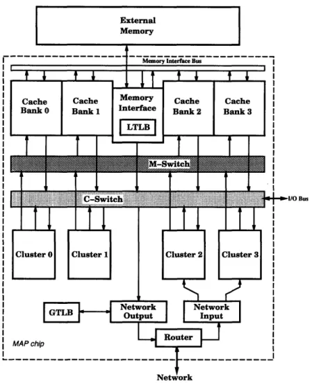
The M-Machine consists of computing nodes that are connected by a 3-D mesh network, where each channel of the network operates at 800 megabytes per second and can transmit in both directions simultaneously. Each of the computing nodes consists of a multi-ALU processor (MAP) chip plus external DRAM. See Figure 1-1 for an illustration of this. The MAP chip itself contains four execution clusters, a memory subsystem, and a communications subsystem. The memory subsystem consists of four cache banks and an external memory interface, while the communications subsystem consists of network interfaces and a network router. There are two crossbar switches that connect the four execution clusters, memory subsystem, and communications subsystem together. One of these switches, called the M-switch, is used to send
0 .0
X-dir -*
Y-dir Z-dir
S
Figure 1-1: M-Machine Architecture
requests from the clusters to the memory subsystem, while the othe switch, called the C-switch, is used to send data from the memory subsystem to the clusters, to send data between the four execution clusters, and to send/receive data via the internode communications subsystem. See Figure 1-2 for an illustration of the architecture of the MAP chip [2].
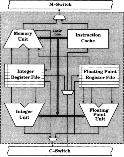
Each of the four clusters is a 64-bit, three-issue, fully pipelined microprocessor. The three functional units found on each cluster are an integer unit, floating point unit, and a memory unit. The memory unit is primarily responsible for sending out load/store requests to the memory subsystem, but it also has the capability to handle many integer operations. Also found in each cluster is an integer register file, a floating point register file, and an instruction cache. One instruction for a cluster consists of up to three operations, one for each functional unit. Each of these operations are issued at the same time but can complete out of order as different
Bus
Figure 1-2: MAP Chip Architecture
operations may have different latencies. See Figure 1-3 for a block diagram of the high level architecture of a cluster [2].
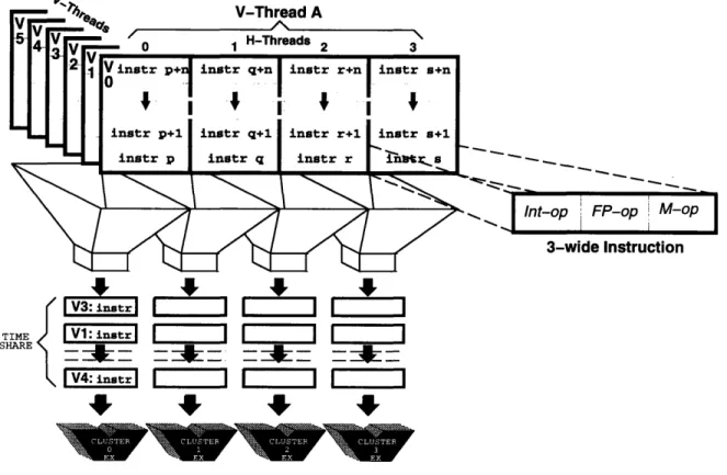
The M-Machine provides the hardware that allows many threads to run con-currently on a node. There are enough resources for six V-Threads, each of which consists of four H-Threads, one H-Thread per cluster. Four of the six V-Threads are user threads, while the other two are for handling exceptions and events. H-Threads can communicate through registers, with each having the capability to write values to the register files of the other H-Threads within the same V-Thread. The H-Threads in a V-Thread can execute as independent threads with different control flows for
Figure 1-3: MAP Chip Cluster Architecture
exploiting loop or thread-level parallelism. On the other hand, the H-Threads can be scheduled statically as a unit to exploit instruction level parallelism, as in a VLIW machine. The V-Threads are interleaved at run-time over the clusters on each cycle. The synchronization pipeline stage handles this by holding the next instruction to be issued from each V-Thread and only issuing an instruction when all of its operands and resources are ready. Since these V-Threads can be interleaved with no delay, switching between threads to mask any pipeline or memory delays can be done with-out any time penalty. This allows the M-Machine to efficiently execute programs with varying granularities of parallelism [1]. See Figure 1-4 for an illustration of the
V-Thread A A. H-Threads 2 3 - - - -3-wide Instruction
4
-1
4
4
4
SV3:
instr
TIME V1: instr SHARE V4: instrFigure 1-4: Relationship of V-Threads to H-Threads
relationship between V-Threads and H-Threads.
1.2
Scope
The MAP pipeline consists of five stages. These stages are instruction fetch, reg-ister read, synchronization, execution, and write back. This thesis will discuss the design and implementation of the execution stage of the integer unit datapath. The execution stage is where the actual integer unit operation is carried out and a result produced. The synchronization stage provides the operands to the integer unit and the instruction information to the integer unit control. The integer unit datapath sends its result to the writeback stage of the pipeline, where the result is written back to the proper destination, as determined by integer unit control.
In developing the design of the integer unit datapath, the instruction set will be
ý L CLU , STER CLUýTE 0 AML
presented as it relates to the integer unit. Much of the thesis will be spent discussing the circuits that were used in the implementation of the integer unit as well as the functionality of the various modules that make up the integer unit datapath. More in-depth circuit studies of Manchester carry chains and zero detection units are pre-sented. Tradeoffs, circuit techniques, alternate designs, and testing strategies will be discussed where relevant.
1.3
Thesis Outline
This thesis is organized as follows. The next chapter will present the architectural de-sign process, the module dede-sign and implementation process, and the testing method-ology that was used. Following that will be a chapter that presents the architectural design based on the MAP instruction set architecture. Then comes a chapter on the actual design and implementation of each of the modules that make up the integer unit. Here, various designs are discussed along with any issues/tradeoffs associated with the different designs. Then the implementations and circuit issues are presented. Finally any testing/verification issues are discussed. The chapter after this presents the testing/verification involved in the integration of the integer unit modules. The final chapter serves as the conclusion to this thesis. The appendices contain such items as the integer unit ISA, some verilog and spice test decks, and the integer unit schematics.
Chapter 2
Design Flow and Methodology
TPhis chapter discusses the process of designing the integer unit datapath. It begins with a section on high level architectural design, followed by a section on individual module design and implementation, and then a section on testing methodology. The chapters following this one present the use of these techniques in actually building the integer unit datapath.
2.1
Architectural Design
When designing a large circuit, such as a functional unit in a microprocessor, the first step is to understand what the unit is supposed to do, how much time it is supposed to do it in, and what its datapath inputs and outputs need to be. In order to figure out what the unit is supposed to do, a good place to start is with the instruction set architecture (ISA). This will give a good idea of what the different tasks are that are expected of the unit to be designed. The amount of time that the unit has to do whatever it is supposed to do is largely determined by the clock rate, the time at which its inputs are available, and the time at which the outputs are needed. The datapath inputs and outputs are largely determined based on the pipeline design of the processor. In the case of the execution stage of the pipeline, the datapath inputs arnd outputs consist of operands and results.
Functional Unit Operands
~/J7
Watr
Functional Unit Outputs
Figure 2-1: Initial Architecture of Example Unit - Module Identification
within the functional unit for each instruction. For example, suppose there is an add instruction. This tells you that the unit will need an adder with a path from the unit's inputs to the adder's inputs. It also tells you that you will need a path to the unit's output. Now suppose you come across a shift instruction. This tells you you need a shifter with paths from the unit's input to the shifter's input as well as a path from the shifter's output to the unit's output. Additionally, assume there is a subtract instruction. This means some kind of a subtraction unit is needed as well. After going through this process for each instruction, you now have an idea of what the major modules within the unit are going to be. See Figure 2-1 for an illustration of this initial architecture.
The next step is to figure out which of the modules can be shared across many instructions and also where muxes are going to be needed. For example, suppose there is an add and subtract instruction. Instead of having a separate adder and a separate subtractor, the adder can easily be turned into an adder/subtractor by adding a little bit of logic and also adding a control signal indicating whether to do an add or subtract. Similarly, suppose an adder and shifter need a path to the output. This implies that the outputs of the adder and shifter can be fed into a multiplexor. The output of this multiplexor could then go to the output. The decision as to whether to select the adder or shifter output can be based on the current instruction and
Functional Unit Operands
Adder/Subtractor
Functional Unit Outputs
Figure 2-2: Intermediate Architecture of Example Unit - Sharing
be conveyed to the mux as a control signal. Therefore, this step reduces the total number of modules needed since sharing can occur. This step also helps with the determination of what control signals are going to be needed. See Figure 2-2 for the new architecture with latches.
The final step in coming up with a high level design is to decide on latch placement.
To do this, a good idea of the delay through each of the modules in the unit is needed,
so this step may be put off until such estimates exist. Generally, the idea is to place the n and p latches in places such that the delay through the logic between each set of latches is about equal. Another factor to keep in mind in deciding where to place the
Adder
Subraor,
Functional Unit Operands
CLK,
I Extra Logic
Functional Unit Outputs
Figure 2-3: Architecture of Example Unit - Latches
latches is the number of bits that need to be latched at each stage. Latches should be placed in locations such that fewer bits need to be latched, thus decreasing the actual number of one bit latches that will be needed. Therefore, there may be a tradeoff between the number of bits to be latched and the amount of logic between latches.
See Figure 2-3 for the architecture with latches place such that the number of bits
that need to be latched is minimized.
After going through these steps, a high level architectural diagram of the unit being designed should be possible to draw. The diagram should show major modules such as adders and shifters, control modules such as muxes, wires between these
SAdder/Subtractor
shift? add/sub?
modules, and control signals needed for these modules, just as in Figure 2-3. The next step is to design and implement each of the modules within the unit.
2.2
Module Design and Implementation
At this point, each module's interface has been defined. The next step is to design and implement each of these modules. Depending on the size of the module in question, further division of the module into submodules may be needed, requiring a procedure similar to the one in the previous section. If the module is simple, such as a mux or latch, implementation is probably the next step. Implementation means the building of circuits at the transistor level.
In designing a module, there are certain things that must be known about the module. These include the inputs and outputs to the module, the speed at which the module must run, and the function that the module is supposed to implement. This information should be enough information to allow for the module to be implemented such that it works correctly and executes at the correct speed.
However, knowing some other things about the "environment" in which the mod-ule will be placed can allow for a more "efficient" implementation in which the circuit may occupy less space, the outputs may have better rise and fall times, and the circuit may dissipate less power. One such factor is knowing the load that this module will have to drive. This is important for a few reasons. The larger the load that needs to be driven, the larger the drive on the output signal has to be in order to have reasonable rise and fall times. Also, the larger the drive needed on the output, the larger the number of stages of buffering that are needed on the output to achieve the desired drive. Since propagating a signal through buffers takes time, the time to carry out the rest of the function is actually reduced as output load goes up. Knowing this information will help save future design iterations. Knowing the load on the output implies that the module to which the output goes has already been designed and/or the length of the output wires are known. For this reason, it is often a good idea to design the module at the end of the unit first and then work backwards towards the
in1
in2
ate
ate out
Figure 2-4: Comparison of Two And Gates
front of the unit. In addition, since large output loads means more buffering in the module being designed, it is often advisable to keep the input load low such that the module that drives this one does not have to do much buffering.
Another factor that is helpful to know which can lead to a "better" circuit is the time at which input signals will be valid. If it is known that some signal will arrive earlier than some others, than it may be possible to do some "precomputation" based on the signals that arrive early. When the late arriving signals finally are valid, there could then be less logic for those signals to propagate through, thereby possibly leading to a faster module. For example, consider a 2-input and gate which consists of a nand gate and an inverter. A static version of the gate could be used if it is not known when the inputs arrive. However, if it is known that one input arrives before another, a pass gate version could be used such that the pass gates are set for the late arriving input. The critical path is therefore decreased. This is a very simple
example but can be applied in many places and many ways. See Figure 2-4 for an illustration of these two styles of and gates.
2.3
Testing
Once a module has been designed, functional verification should be carried out before sizing transistors. This will save time especially as functional bugs are found that cause the circuit to have to change. After verifying functionality, then transistor sizing can take place. At this point, timing verification needs to take place. The following sections discuss both functional and timing verification techniques.
2.3.1
Functional Testing
The first step in verifying a module is to make sure that functionally the circuit is doing what it is supposed to do, i.e. the outputs of the circuit for each given set of inputs matches what the outputs should be. In doing functional verification, the delay through the module is not the main concern.
For a circuit to be truly functionally verified, every possible set of inputs would need to be run on the circuit. Often this is not practical, such as when trying to verify a 64 bit adder, due to the extremely large number of possible input combina-tions. In these cases, the following procedure, once completed, should leave the tester reasonably confident that the circuit is functionally correct.
The first step in the functional verification procedure is generally to run hand-crafted test cases through a module, making sure that the module passes these tests. These hand-crafted cases should at the very least test every part of the circuit. This is called glass-box testing, since the tester has to know what is inside the "box" in order to test all parts of it. By testing every part of the circuit, it is meant that for each part of the circuit there is at least one set of inputs such that the output depends on the proper operation of that part of the circuit. In this way, every part of the circuit is "exercised". This kind of testing is often useful for determining such things as where connections are missing, where connections are switched, and where
there are logical errors.
Running hand crafted cases often only tests a very small percentage of all of the possible input combinations. The more input combinations that are tested, the more confident a tester can be that the circuit is logically correct. Therefore, the next step in functionally verifying a circuit is to run a randomized test. Here, a program is written that generates random inputs and feeds them into the circuit. The outputs can be checked versus the results of running the same inputs through a behavioral model of the circuit. If the results differ, then the errors should be logged so the tester can go back to the circuit and figure out the problem. By letting this simulation run for a long time (several days, depending on the number of possible input combinations), many more inputs can be run through the circuit than by doing only glass-box testing. This kind of testing is more of a black-box strategy, since the tester does not necessarily need to know the actual implementation of the circuit in order to test it. In glass-box testing, the tester must know the circuit in order to test each part of it.
Doing glass-box and black-box testing will not guarantee that a circuit is func-tionally correct if all possible inputs are not tested. However, it will leave the tester more confident of the circuit. This confidence level goes up as more testing is done.
2.3.2
Timing Verification
Having verified functionality of a circuit, the next steps are to size the circuit and run timing tests to see that the circuit meets the timing constraints that have been placed on it. The timing tests for the integer unit were run using HSPICE. HSPICE is a tool which basically takes in a netlist representing the circuit to be tested, a model representing the process to be used, and a stimulus file which contains the inputs to be run through the circuit. The output can be viewed graphically using a tool such as GSI. The output, when viewed using GSI, consists of the waveforms at various nodes in the circuit, including the inputs and outputs. From these waveforms, the delay through a circuit to various nodes and the rise and fall times of signals at various nodes in the circuit can be determined.
Since simulations using HSPICE often take a relatively long time to run as com-pared to simulations for functionality using something like Verilog, a significantly smaller number of timing simulations can be run. It is important to simulate each path through a miodule. If that is not practical, then it is more important to simulate those paths which potentially may have the longest delays. These long paths can often be determined from looking at the circuit schematics.
Since these simulations should indicate what the delay through the circuit will actually be when the chip is fabricated, it is important that the simulation take into account such things as wire length, parasitics, and output loads. In order to estimate these, the tester needs to have an idea of where the module being tested will be sitting in the overall floorplan and how large the various modules will be. The tester also needs to know what the outputs will be driving. From this information, wire lengths and loading can be estimated and added into the stimulus file. Without adding this information, simulations would underestimate the amount of delay through a module. It is generally better to overestimate, as opposed to underestimate, loads, thus leading to overestimated delays. That way, if the circuit can meet the timing constraints with the overestimate, it can definitely meet the timing constraints when the actual fabricated circuit is used. However, if underestimated loads are used in the simulation resulting in underestimated delays, it is possible that the fabricated circuit may not meet the timing constraints.
Therefore, timing verification consists of determining wire, gate, and parasitic loads, adding these numbers into the spice deck, simulating the critical paths through the circuit, checking to make sure the delays meet timing constraints, and making sure that the rise and fall times of all signals are reasonable. If the timing numbers are not reasonable, that may mean going back and resizing the circuits and then resimulating again. If it is determined that the timing constraints cannot be met using the current design, then that may entail redesigning, reverification of functionality, and reverification of timing.
Once satisfied with the verification process, the circuit is layed out. On completing layout, more precise numbers for wire, gate, and parasitic loads become available.
Module
Figure 2-5: Design and Testing Flow
These numbers should be corrected in the spice deck that was previously created, and timing verification should be redone to make sure that the circuit is still operating correctly and is still fast enough to meet constraints.
See Figure 2-5 for an illustration of the design and testing flow. As the figure shows, there may be several iterations of many of the steps.
2.3.3
Variations in Verification Styles
Due to the possibility of having to redesign and reverify functionality after finding that the circuit is not meeting timing constraints, it may seem that a lot of needless time was spent in functional verification before timing verification was even reached. For this reason, it may be more reasonable to follow a different procedure in testing a module.
rification
Architectural Desian
Unit Tes
Figure 2-6: Integer Unit Design Flow
This better procedure would be to do glass-box testing first, as before, and then move on to timing tests after sizing the circuits. At this point, if it seems that timing will not be a. problem, then the functional verification can be continued at a more thorough level in parallel with the timing verification. This may save time since a more unreasonable design from a timing viewpoint can be detected earlier, thereby saving the time it would take to do the full functional verification.
2.4
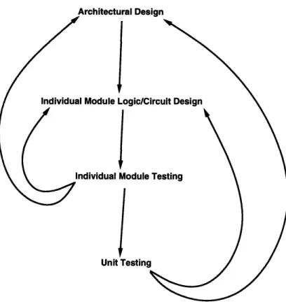
Summary
In summary, the design of the integer unit datapath began with design of the overall architecture. In this step, the necessary modules and interconnections were determined. Next, design of each module was done, determining the kind of logic each module would require, followed by circuit design of each module. Finally came
I
Logitesting of each individual module, testing of groups of modules, and then testing of the whole integer unit. See Figure 2-6 for an illustration of the design flow.
Chapter 3
Integer Unit Architecture
This chapter presents the high level design of the integer unit. It develops the archi-tecture by going through the ISA and then determining what modules are needed, what modules can be shared, and what control signals are required. At that point,
the high level architecture of the integer unit datapath will be complete. The first section presents a high level specification for the integer unit.
3.1
Integer Unit Specifications
The integer unit is one of three functional units in each cluster of the MAP chip. The
integer unit is part of the execution pipeline stage, which follows the synchronization pipeline stage and precedes the writeback pipeline stage. Since the chip has a 100
MHz clock, the integer unit has O10ns to do whatever it has to do1. The integer
unit datapath takes in two source operands and the instruction pointer from the synchronization stage. It outputs the result to the writeback stage, whcih in turn sends the result to the integer register file. The result and source operands are 64 bit two's complement numbers.
The addresses are actually 54 bits wide with the remaining 10 bits having special meanings. The top four bits indicate what kind of pointer the address is. The next
'If the integer unit needs more time, it may be able to borrow time from an adjacent pipeline
six bits are used to indicate the size of the memory segment containing that address. These six bits are used for such things as doing segment boundary violations for address calculation.
3.2
The Major Modules
In this section, the ISA will be used to determine what major modules will be needed in the integer unit. See the appendix for a complete listing of the integer unit in-struction set.
The first batch of instructions in the integer unit ISA is the arithmetic operations. These operations include add, add unsigned, subtract, subtract unsigned, arithmetic shift, logical shift, rotate, and, or, xor, and not. The add operations imply the need for an adder that takes in two 64-bit inputs and outputs the sum to the writeback stage. The adder also outputs some overflow information that should go to control. The subtract operations imply the same thing as the add operations, except we need a subtractor instead of an adder. Recognizing that a subtractor can be implemented as an adder that inverts its second operand and adds one to the output, the adder can be used to serve as a subtractor as well. This is possible when the operands are two's complement values. Therefore the adder would need a control signal to indicate when to subtract. When this signal is asserted, the adder should invert the second operand and set an internal carryin to high.
The shift and rotate operations imply the need for some kind of a shifter that takes in one 64-bit input along with control information about how much to shift, in what direction to shift, and whether to wrap around in the case of rotate. It outputs a new 64-bit value that should go on to the writeback stage.
The boolean operations imply the need for some sort of boolean unit that takes in two 64 bit operands and control information representing the function to carry out. The output would be sent on to the writeback pipeline stage.
The next batch of instructions are the byte manipulation operations. These in-clude extract byte, extract halfword, insert byte, and insert halfword. The extract
operations consist of taking a particular byte or halfword from one source and putting it in the low byte or halfword of the result. This implies the need for shifting to move the byte or halfword to the appropriate place in the result and a need for some sort of selector to pass either the byte, halfword, or zero. The insert operatons consist of moving the byte or halfword in the low bits of one of the sources to a particular location in the other source. Again, this implies the need for a shifter and selector. The shifter can be the same as that used for the shift operations. The selector can be placed at the output of the shifter. It would need such control signals as whether to pass the shifter output, the source input, or zero depending on the operation being performed.
The comparison operations compare the two operands checking for such things as equality, greater than, or less than. A way to do comparison operations is to subtract the two operands and run the results through a zero detector. The result of the zero detector in combination with the overflow information that comes from the adder/subtractor can then be used in control to decide the result of the comparison. Therefore, comparison operations require an adder/subtractor, which was already needed, along with a zero detector that takes in the result of the adder/subtractor.
The output of the zero detector would go to control. No additional control inputs
are needed for the adder, and no control inputs are needed for the zero detect. The result of the comparison operation, which will come from control, needs a path to the output of the integer unit. This result will go to a condition code register and will be referred to as cc.
The next class of instructions is the data movement instructions. The integer unit does not have to do much with these instructions except to pass values from the input to the output. Therefore, no special modules are needed to handle these instructions. There just has to be a way to pass inputs straight through the integer unit unchanged. This can be done in many ways such as passing the input through the shifter unchanged or passing the input through the boolean unit unchanged.
The only control flow operation that requires any kind of computation is the branch instruction, whereby IP and src2 have to be added together. The adder that
is already needed for other operations can again be reused. However, now since the operands for the adder depend on what instruction is being executed, a multiplexor will be needed in front of the first input to the adder in order to select between the IP and srcl. A control signal for the multiplexor will select the proper operand based on the instruction.
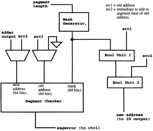
The address calculation operations include lea, leab, and some pointer operations which write condition codes. The lea operation consists of adding an immediate to an address and making sure that the resulting address is within the same segment as the original address. This implies the need for an adder and for some way to check that the new and old address are within the same segment. One way to check this is to generate some kind of mask that indicates which bits of the old and new address must be the same, based on the 6 segment size bits from the original address. This mask, in conjunction with the old and new address can then be used to determine if there is a segment violation. Therefore, an adder, mask generator, and segment checker are needed. The adder already exists.
The leab instruction is similar to lea except that an immediate is added to the segment base of a given address. Then a segment check is done on the new address. Therefore, some way is needed to generate the segment base. This can be done by masking out the bits from the original address that are allowed to change and still result in an address that is in the same segment. Having done that, the integer to be added to the base can be logically or'd with the segment base, thus resulting in the new address. To do the segment check, a mask, old address, and new address is needed. The mask can be generated by the mask generator, the new address would
be the immediate to add to the segment base, and the old address could be zero. If any bit in the new address outside the mask area is not zero, the segment checker
would detect this and signal an error. Therefore, this instruction requires two boolean units, a mask generator, and a segment checker. However, the address inputs to the segment checker for leab are different that those for lea, so muxes would be needed
at the address inputs to the segment checker. Also, a path would be needed from the mask generator to the first boolean unit. The other input to the first boolean unit
segment
2
Figure 3-1: Modules needed to execute leab
would be the first source input to the integer unit. The second boolean unit would take in the output of the first boolean unit and the second source input to the integer unit. Boolean operations could still be done by passing the source input through the first boolean unit and carrying out the actual boolean operation in the second boolean unit. See Figure 3-1 for an illustration of the modules needed to execute an
leab instruction.
The pointer operations in the address calculation class of operations simply require a place for a condition code to enter the datapath and be passed through to the output. No computation module is needed in the datapath for these operations.
There are two immediate operations. The create immediate operation requires a pass through path, which is already needed by some previous instructions. The other operation, called the shift & or unsigned 16-bit immediate, requires one input to be shifted 16 bits and then an immediate to be placed in the low 16 bits. This means a
shifter and some kind of inserting mechanism is required, both of which already exist as a shifter and selector. Therefore, no new modules are needed for the immediate class of operations.
The configuration space operations consists of only the GTLB access instruction. This operation is similar in function to the operations in the communications class of operations, which is the final class of operations. The general idea behind the communication operations is to send a series of values onto the C-switch, which is the switch on which clusters can communicate with each other and on which data from memory is returned to the clusters. The sources of the values to send over the C-switch are both of the integer unit source inputs followed by data off of the writeba.ck line that goes to the writeback stage. The writeback line is actually an input/output line over which data is sent to and from the register file. Therefore, to execute these instruction requires a mechanism for sending these values, one at a time on each clock cycle. This implies muxes and latches, all of which will need to be placed in a separate computation module that takes in the two source operands as well as the writeback line. The output of this "send" unit would need to go to the C-switch.
All of the instructions have now been accounted for. However, the integer unit also needs to take care of passing exception and "errval" identifiers. An "errval" is basically a deferred exception. Generally, an errval is created by passing the IP to the writeback stage, where the IP pointer type has been modified to reflect an errval and some information about the type of errval has been added in the six bits usually associated with segment length. Therefore, a path is needed from the IP to a module which composes the errval to be sent to the output. Finally, exception identifiers are simply 10 bits that also need an entry point to the datapath from control and then a path to the output whenever an exception occurs. However, these 10 bits do not need to be combined with any other piece of data, unlike the errval.
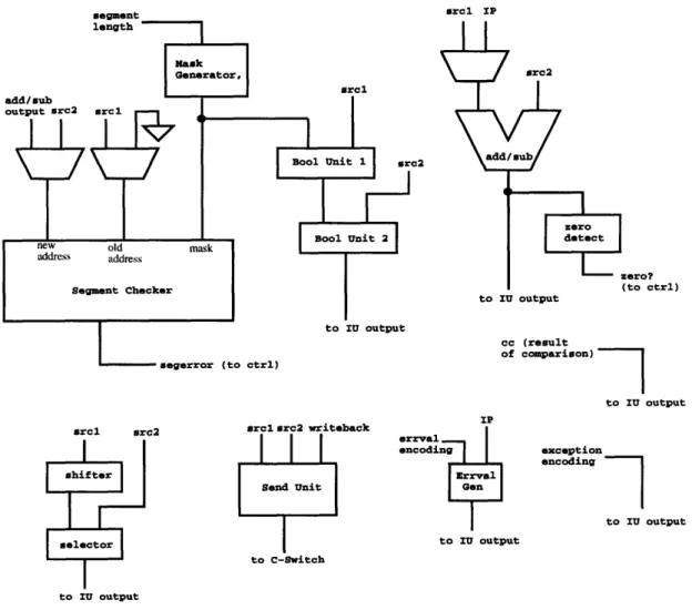
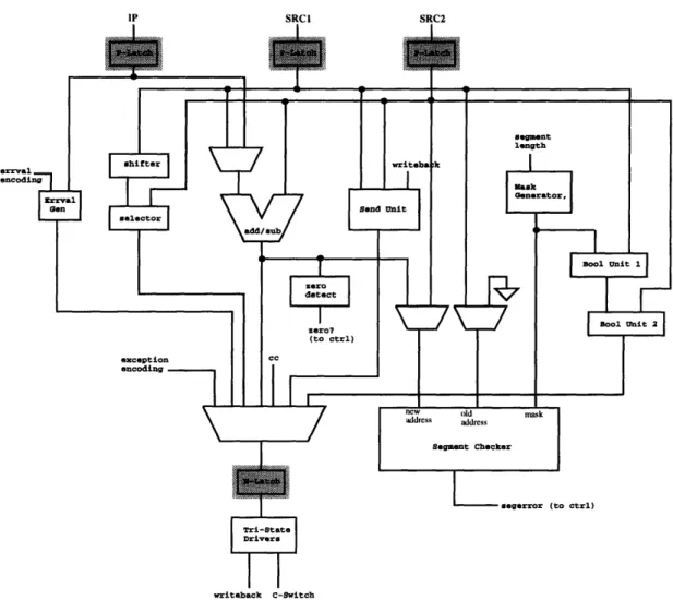
Therefore, the major modules that will be needed include an adder/subtractor, shifter, selector, zero detector, two boolean units, mask generator, segment checker, send unit, and errval generator. See Figure 3-2 for an illustration of this temporary
segment src2 to arcl src2
I
shifter selector to IU output srcl src2 writeback Send Unit to C-witch to C-Switch IP trrval encoding Errval Gen to IU output zero? (to ctrl) IU output cc (result of comparison) to IU output exception encoding to IU outputFigure 3-2: Intermediate integer unit architecture
architecture. In the next section, these modules are put together to form the integer unit, datapath.
3.3
Putting It All Together
Now that all of the needed major modules have been identified, the next step is to put them together along with muxes, latches, and drivers, in order to form the integer unit datapath.
Many of the major modules share the same inputs, so running the inputs to each of these modules needs to be done. Also, many of these modules want to send their
SRC2
Figure 3-3: Intermediate integer unit architecture with output mux
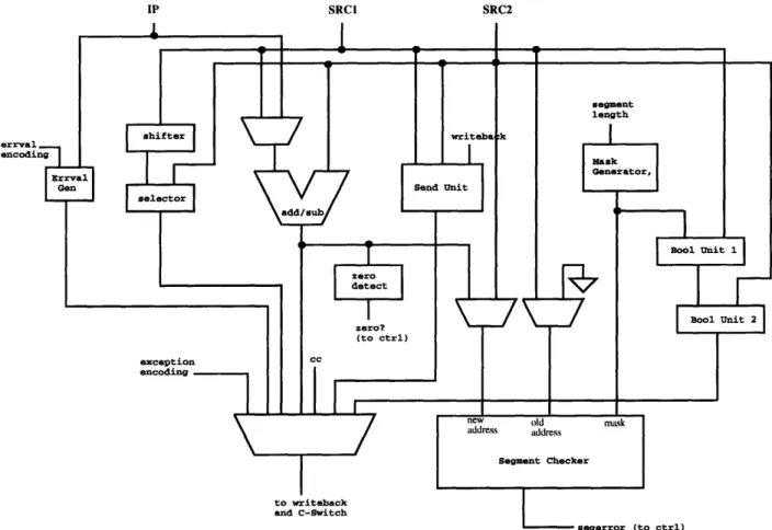
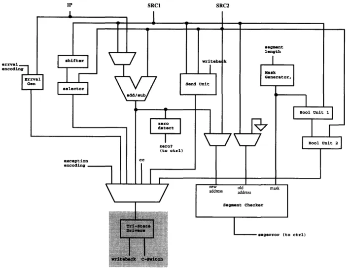
outputs to the integer unit output. A mux is needed on the output line to select between the various modules that are driving the output. The line to select would be based on things such as the operation being performed and whether there was an exception or an errval to pass. See Figure 3-3 for the updated integer unit architecture. The results of the integer unit instructions either go to the C-switch or the integer register file. However, the line to the integer register file drives data in both directions, so the module driving the output has to have a state capability. Therefore, a tri-state driver is need to drive the outputs of the integer unit to the register file and C-switch. See Figure 3-4 for the updated architecture.
At this point, the integer unit architecture is nearly complete. However, the n-latches and p-n-latches need to be added. The strategy here is to place n-latches such
SRCI SRC2
Figure 3-4: Intermediate integer unit architecture with result driver
that few bits have to run across the latch and such that the amount of logic between latches takes up about half of a clock cycle. Without knowing the actual delays through each of the major modules and looking more at having a low number of bits needing to be latched, it appears that the best latch placement would be p-latches at the inputs to the integer unit and n-latches after the mux that selects the output to go to the driver. This will probably result in a larger amount of logic between the p-latches and n-latches than between the n-latches and the next set of p-latches in the next pipeline stage. However, the amount of logic between the n-latches and p-latches will hopefully have a delay that is low enough such that there is no timing
IP a SRCI SRC2
I
_
-Tri-State DriversI
I
writeback C-SwitchFigure 3-5: Intermediate integer unit architecture with latches
issues here. If not, then some time can be borrowed from the logic that follows the n-latch. See Figure 3-5 for an illustration of the latch placement in the integer unit.
One final issue has to do with the timing of deciding when to pass an errval. In some cases, the decision to pass an errval may not occur until after the second half of the clock cycle. It would probably be beneficial to place the errval as close to the output as possible such that it has to propagate through less logic in the case that it is selected. This can be done by placing a 2-input multiplexor between the n-latch and the driver, where the two inputs would be the latched output of the previous tmultiplexor and the errval line. Since the errval has no n-latch in its path, another
Tri-Stato
Drivers
writeback C-Switch
Figure 3-6: Final integer unit architecture
n-latch would have to be added on the errval line. At this point, the integer unit datapath architecture is complete. See Figure 3-6 for the integer unit architecture.
Chapter 4
Integer Unit Submodules
The following sections provide descriptions of each of the major submodules within the integer unit. The purpose, design, and implementation of each module is presented. Also, any issues/tradeoffs that led to a particular implementation are discussed.
4.1
Adder/Subtractor
The adder/subtractor that has been implemented is a hybrid carry lookahead/carry select adder. It takes in two 64-bit operands, along with sub and carryin, which are control signals. In the rest of this section, a and b will refer to the two operands. The output is another 64-bit value, which will be referred to as out, along with two bits which go to control. These two bits are called gc8 and gc7 and are used by the integer unit control to detect overflow.
In order to understand how the adder works, first consider the addition of two one-bit numbers with a carryin input and a carryout output. Without knowing what the carryin signal is, it is known that carryout will be 1 if both operands are 1,
carryout will be 0 if both operands are 0, and carryout will equal carryin if one of the operands is 1 and the other 0. These three cases are called generate, kill, and propagate, respectively and are easily computed through use of an and gate, nor gate, and xor gate, respectively.
signal, since it is possible to set up a chain structure that allows carryin to propagate up through the chain for each pair of bits very quickly. This in turn allows for quick
sum calculations once carryin is known. To calculate the sum bit, all that needs to
be done is to xor the carryin and propagate bits for each pair of input bits.
A very slow adder could be built which creates a chain going across all 64 bits. This would be slow since carryin would potentially have to propagate through at least 64 transistors. The adder implemented in the integer unit instead does some speculative computation of sum bits and then selects the appropriate results, such that the longest chain that any carryin has to propagate through is a chain of 8 transistors.
Basically, after computing generate, kill, and propagate for each pair of bits,
gen-erate, kill, and propagate are computed for each of 8 groups of 8 bits. From these
group signals, group carries can be computed for each group of 8 bits. While the computation of these group signals is going on, local carries for each of the 64 pairs of bits are computed in groups of 8 bits assuming carryin of both 0 and 1, thus resulting in 128 local carry signals. These 128 signals are then xor'd with the corresponding
propagate bits to generate 128 sum bits. The proper 64 bits to output are chosen
based on the group carry signals, since these indicate whether the correct carryin for each local group of 8 bits was a 0 or 1.
See Figure 4-1 for a block diagram of the adder architecture. The pgkblock com-putes 64 sets of generate, kill, and propagate signals, which go to the group pgk block and to the local carry chains. The group pgk block calculates group generate, group
kill, and group propagate for each group of 8 bits, sending its results to the global
carry chain, which calculates group carries. The local carry chains, of which there are 2 for each group of 8 bits, computes local carry signals assuming carryins of 0 and 1. The outputs of both the global carry chain and local carry chains, along with individual propagate signals, go to the final cell where sum bits are computed and then selected based on the group carries.
The worst case delay through the adder is about 3.7ns. This occurs when carryin is 0 and each pair of bits being added together has a 0 and a 1. The following sections
sum su
Figure 4-1: Block diagram of adder internals
describe each of the modules in detail.
4.1.1
PGK Block
The pgk block is the module into which the 64-bit operands flow. It also takes in the sub control signal. Recall, when doing a subtract, b needs to be inverted and carryin needs to be set to 1. The pgk block does the necessary inversion in the case where a subtract is being done. The purpose of the pgk block is to compute propagate,
generate, and killL, for each of the 64 pairs of input bits as follows:
propagate = a ( bnew
generate = a&bnew killL = albnew
where bnew is equal to b if a normal add is being done, else bnew is equal to the inverse of b in the case of a subtract operation. See figure 4-2 for a block diagram of
b
kL
p
g
Figure 4-2: Block diagram of pgk block internals
the pgk block. The adder contains 64 instances of this module, one module for each pair of bits.
Of the three operations that need to be done in this block (xor, and, or), xor is the most time consuming and is therefore on the critical path through the pgk block. Therefore, different xor gates were looked at before one was selected. The options that were tested include a static branch based version and a pass gate version. Additionally, one other experiment was tried for evaluation of propagate. By noting that propagate = generate&killL, the xor gate can be eliminated in favor of an and gate.
See Figure 4-3 for the schematic of the pass gate version of the pgkblock. Note that each transistor has its relative width printed next to it in this and all schematics. The pass gate version consists of two n-only pass gates which pass a or d depending on the value of b. The value of b will be known earlier than that of a since there is a mux in front of the adder on the a input, as can be seen in the integer unit architecture. This knowledge is useful since b can then be used to select the pass gate such that the pass gates will be ready to pass the a input when it becomes valid. Following the pass gates is a low threshold inverter to equalize the rise and fall times on the
Figure 4-3: Schematic of pass gate version of pgk block
This occurs when a and sub are high with b going from high to low.
See Figure 4-4 for the schematic of the static gate version of the pgkblock. The static gate version of an xor consists of 8 transistors, requiring both senses of a and b at the inputs to the xor gate. In the worst case, the output needs to be pulled Iup through two PFETs. The worst case delay through the pgk block using this gate was 760ps. This happens when a is low, sub is high, and b transitions from low to high. This circuit takes up more area than the pass gate version and also has rather large transistors in the static xor gate. This in turn causes the load on the xor input lines to be large compared to the pass gate version. Given that the load on the pgk block inputs is kept the same for both the pass gate and static gate versions of the
pgk block, the delay through the static gate version will be larger due to the higher
internal load.
See Figure 4-5 for the schematic of the pgkblock which does not use an xor gate. The final version, which does not use an xor gate, simply gates the generate and kilLL signals together to derive propagate. The worst case delay through this circuit is 920ps, occurring when a and sub are low with b going from high to low. The nice
Figure 4-4: Schematic of static gate version of pgk block
thing about this circuit is the reduced load on the internal a and b lines. However, the evaluation of the propagate signal cannot begin until generate and killL are known, thus causing the large worst case delay.
From these experiments, it is clear that the best version to use is the pass gate xor version. Not only is this the fastest of the three, but also it uses the least area.
4.1.2
Group PGK
The group pgk module is responsible for taking in eight sets of propagate, generate, and killL signals, corresponding to a group of 8 bits. It uses these 24 input signals to compute group generate, group propagate, and group killiL, which will be referred to as gg, gp, and gkL, respectively. The purpose of computing these signals is to allow for group carries to be computed in the next stage. These group carries will be used to select the proper local carries in the final stage. There are 8 of these modules in the adder, thus accounting for all 64 bits.
When gp is asserted, this indicates that the carry output from this set of 8 bits should be whatever the carry input is. This signal should be asserted if all of the
Figure 4-5: Schematic of non-xor version of pgk block
8 input propagate bits are asserted. This requires an 8 input and gate. The actual implementation is two 4-input nand gates followed by a 2-input nor gate. Using an 8-input gate is not reasonable due to the long chain of transistors that would result. The delay through a long chain of transistors can become very high, and the resulting output waveform can have very bad rise and fall times. In addition, transistor sizes can get very large when trying to achieve reasonable delays.
When gg is asserted, this indicates that the carry output for this set of 8 bits should be asserted no matter what the carry input is. The circuit that is used to compute this is a Manchester carry chain. Based on the values of the input propagate, generate, and kilLL signals, gg can be computed. Each "link" of the chain basically consists of three transistors, each controlled by one of 8 sets of propagate, generate, and kilLL. The idea is to pass a 0 up to the next "link" in the chain if the carry out for the bit being looked at is a 0, and to pass a 1 if the carry out is a 1. At the top of the chain, if the output is a 1, then that indicates that the carry output for the group is a 1. Therefore, for a particular "link", if generate is asserted, then a 1 should be passed on to the next chain. If kilLL is asserted, then a 0 should be passed on. Otherwise,
carryL (to next link) generate kill_L
propagate
carry_L
(from previous link)
Figure 4-6: Illustration of a typical link in the carry chains
if propagate is asserted, then the value being passed from the previous "link" should be passed on to the next link. This indicates a "link" that looks like that shown in Figure 4-6. Note that in this figure, the inverse of carry is passed up the chain, meaning if generate is asserted, it would pass a 0, and vice versa for kilLL. See the actual schematic later in this section.
Since there are 8 bits in a group, the chain would consist of 8 of these links. Eight of these links together means there would be 8 transistors in series. This may or may not be a problem in terms of the size these transistors would have to be and the speed at which this circuit would run. If it turns out there is a size of speed problem, one thing to try would be putting a buffer in the middle of the chain. Another idea is splitting the chain, making the top part of the chain speculative, and using the result of the bottom part to select the proper results from the top part of the chain.
Before going on to present the different ways for setting up the carry chain, the evaluation of gkL will now be discussed. Actually, all that is need to evaluate gkL is to realize that gkL = gplgg. Therefore, gkL is not evaluated until gp and gg have been determined. However, since gp will be ready earlier than gg in the worst cases, the gate used to generate gkL is set up to expect gp to be early, thus saving some time. This is done by placing the gg input to the nor gate at the transistors closest to the output of that gate, which is a standard technique for taking advantage of early