HAL Id: hal-02151291
https://hal.archives-ouvertes.fr/hal-02151291
Submitted on 7 Jun 2019
HAL is a multi-disciplinary open access
archive for the deposit and dissemination of
sci-entific research documents, whether they are
pub-lished or not. The documents may come from
teaching and research institutions in France or
abroad, or from public or private research centers.
L’archive ouverte pluridisciplinaire HAL, est
destinée au dépôt et à la diffusion de documents
scientifiques de niveau recherche, publiés ou non,
émanant des établissements d’enseignement et de
recherche français ou étrangers, des laboratoires
publics ou privés.
optimization of the nSiC layer’s thickness in a nSiC/Si
photovoltaic cell
M Kabe, Y. Lare, L. Ottaviani, M. Pasquinelli, D Barakel
To cite this version:
M Kabe, Y. Lare, L. Ottaviani, M. Pasquinelli, D Barakel. M. Kabe and al. / Simulation and
optimization of the nSiC layer in a nSiC/Si photovoltaic cell Simulation and optimization of the nSiC
layer’s thickness in a nSiC/Si photovoltaic cell. Materials and Devices, Collaborating Academics –
International Press, 2019, 4 (1), �10.23647/ca.md20193103�. �hal-02151291�
Article type: Conf.-Conference paper (CASAMANSUN2018)
Simulation and optimization of the nSiC
layer’s thickness in a nSiC/Si photovoltaic cell
M. Kabe (1), Y. Lare (1), L. Ottaviani (2), M. Pasquinelli (2), D. Barakel
(2), M. Portail (3)
(1) Solar energy laboratory, University of Lome, Togo
(2) IM2NP (UMR CNRS 7334), Aix-Marseille University, France
(3) CRHEA (Research Center of HeteroEpitaxy and its Applications), Nice, France
Corresponding author:
[email protected]
RECEIVED: 1st april 2019 / RECEIVED IN FINAL FORM: 1st june 2019 / ACCEPTED: 3rd june 2019
Abstract : Simulations of the emitter layer in 3C-SiC heterostructure solar cells were performed by means of SCAPS to model the optimal thickness and predict the influence on cell’s behaviour. Then, the cells have been elaborated by chemical vapor deposition and characterized. The opto-electrical measurements showed an improvement of the absorption of photons in the short wavelengths thanks to the thin layer of the emitter, and the non-degradation in bulk of the base cell. On the front side, the using of Ti/Au contacts also leads to an improvement in the absorption of photons thanks to the low series resistance.
Keywords : SiC thin layer, heterostructure, solar cell
Introduction
Silicon remains the most used material in photovoltaic field. However, its applications are limited in the visible photo-conversion range. Thus, research is venturing into experimenting with wide band gap semiconductors such as silicon carbide in order to widen the spectral band from visible to ultraviolet, by using the polytype 3C of the silicon
band gap semiconductor material with exceptional properties in terms of temperature resistance, and chemical stability. 3C silicon carbide, with 2.36 eV bandgap could be a potential candidate and also, this material has been extensively studied due to its potential applications in variety of fields (1). SiC is known for its ability to resist to high radiation level (2), making it suitable to work in solar concentrators. 3C-SiC/Si heterojunctions have
Cite this article: M. Kabe , Y. Lare, L. Ottaviani, M.
Pasquinelli, D. Barakel, M. Portail, OAJ Materials and
Devices, Vol 4 (1), 3103 (2019) – DOI:
diodes (3), as window layer or as emitter for photovoltaic cells in several configurations (4). The opportunity to make 3C-SiC/Si tandem cells has been studied theoretically (5) even if according to
(6), a tandem cell formed of an SiC cell superimposed on a silicon cell would hardly achieve the performance of a single silicon cell. The first step in order to realize 3C-SiC/Si tandem cells is to masterize the deposition of 3C-SiC on Si wafers.
We carried out simulations first in order to optimize the emitter layer to have a better conversion of the photons in the field of ultra-violet, and to understand the degradation of the Si bulk properties during the SiC film deposition. Then, characterizations were performed on cells developed by the CRHEA (Center for Research on Heteroepitaxy and its Applications). The present work presents the results.
Simulation results
In order to predict the properties of the cells to be developed by CRHEA, we performed simulations using SCAPS software. SCAPS is a software for modeling solar cells based on CdTe and CIGS (7), developed by Marc Bulgerman of the Department of Electronics and Information Systems (ELIS), University of Gent, in Belgium. Our simulations thus consisted in the optimization of the emitter layer of the heterojunction 3C-SiC/Si. We optimized also the influence of the diffusion length of the carriers in the bulk of Si following the deposition temperature during growth of the SiC/Si deposition process by the CVD method.
Figure 1: Influence of SiC thickness on EQE
Figure 2: Influence of the lifetime in the Si bulk
These simulations have shown, first the improvement of the spectral response in the short wavelengths, especially for an optimal thickness of the emitter of 0.2 μm. Secondly, a degradation in the visible response for >600nm could be observed in the bulk of Si during the growth of SiC, Similar results were obtained by Touré et al (8).
Results and discussions
Samples
3C-SiC, <100> oriented, epitaxial layers were grown on <100> oriented, 10 ohm.cm p-type silicon wafer by resistive heating hot wall chemical vapor deposition, under Hydrogen flux (15sml). Silane and Propane gases were used as precursors, under 200 mbar of pressure (C/Si ratio =1.1). Nitrogen was used in order to produce an n-type doping. The growing has been realized in two steps, first a carburation step at 1100°C, then a growing step at 1350°C. This process has been described in (9). The Nitrogen flux for the doping level was 50 sccm, producing an estimated doping level of 7-8* 1018 cm-3 and 1019 cm-3.The two highest doping levels have been controlled by FTIR method (10). The thickness of the emitter is varied: 2 μm, 1 μm, 0,5 μm, and 0,2 μm. One wafer was doped at 1019cm-3.
Photovoltaic cells were then produced in three steps: (i) Mesa-structures were realized by classical photolithography (Size 1.98x2.43 mm), (ii) the Ti/Au front contacts were deposited followed by a subsequent annealing at 460°C, (iii) an Al/Au layer was deposited on the backside of the wafer, followed by an annealing at 460°C. Some other cells were fabricated using Ni/Au as ohmic contacts on the front side.
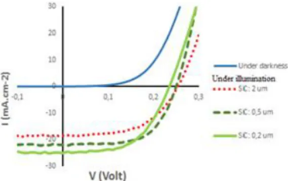
Current-voltage characteristics
Current-Voltage measurements were performed using a Keithley 236 source-measurement unit. The curves in the dark are fitted with a single diode model based on the series and the shunt resistances, the ideality factor and the saturation current. A solar simulator with an AM 1.5 spectrum and an illumination power of 1000 W.m-2 allows
measurements under light.
.
Figure 3: Current voltage characteristics
The parameters of the cells are presented in table 1. Table 2 shows the previous results obtained by Moussa and al, with diodes based on 2 um SiC emitters and distinct doping levels (from 4.1017 cm-3 to 3.1019 cm-3) and
Ni/Au layer as ohmic contact on front side (8).
Table 1: Parameters of the new diodes
Emitter layer Voc (mV) Jcc(mA.cm-2) FF(%) η (%) Rs(Ω) Rsh(Ω)
0,2 μm (7.1018 cm-3) 220 ± 8 23,66 ± 0,56 0,502 ± 0,062 2,8 ± 0,4 27,625 ± 7,06 1247,83 ± 202,77 0,5 μm (7.1018 cm-3) 245±1 21,62 ± 0,12 0,58 ± 0,039 3,1± 0,12 20 ± 10,42 2906,53 ± 1675,86 1 μm (7.1018 cm-3) 260 ± 7,5 16,27 ± 0,52 0,62 ± 0,01 2,63 ± 0,13 12,31 ± 0,126 4359,42 ± 1175,82 2 μm (7.1018 cm-3) 260 ± 3,8 18,49 ± 0,12 0,52 ± 0,012 2,5 ± 0,12 56,88 ± 18,93 1194,27 ± 399,065 n+, 2 μm (1,5.1019 cm-3) 270± 1 16,66± 1,04 0,5 ± 0,01 2,37 ± 0,12 75,5 ± 8,74 1784,7 ± 136,6
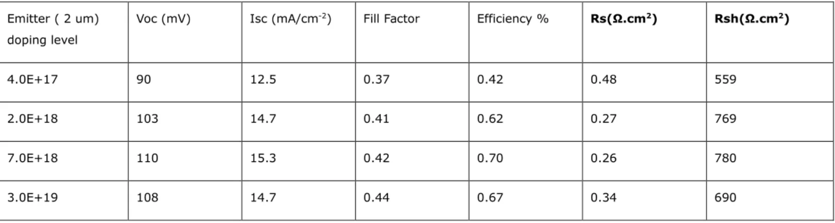
Table 2 : Parameters of the former diodes (8) Emitter ( 2 um)
doping level
Voc (mV) Isc (mA/cm-2) Fill Factor Efficiency % Rs(Ω.cm2) Rsh(Ω.cm2)
4.0E+17 90 12.5 0.37 0.42 0.48 559
2.0E+18 103 14.7 0.41 0.62 0.27 769
7.0E+18 110 15.3 0.42 0.70 0.26 780
3.0E+19 108 14.7 0.44 0.67 0.34 690
One wafer with 2 μm SiC layer and a specific doping value of 1019 cm-3 was also developed by
CRHEA. It can be noted that all the parameters of the cells with thicknesses lower than 2 μm are better, since the average quantum efficiency reaches 3%. In addition the highest photocurrent of the order of 24 mA.cm-2, is related to the lowest
thickness of the emitter layer (0,2 μm). The metallization of the front contact using Ti/Au rather than Ni/Au leads to two phenomena: the reduction of Rs and increasing of Rsh on one hand, the
improvement of Voc on the other hand. Nevertheless, the Voc remains weak, indicating that
the recombinations at the interfaces are not negligible.
External quantum efficiency
The benchmark of quantum efficiency, is based on a Xenon UV-extended arc lamp, able to emit light from 200 to 1180 nm wavelengths, a monochromator, a chopper and a lock- in amplifier. The illumination power ranges from 80 nW cm-2 at
200 nm to 10 μW cm-2 from 400 to 1180 nm. The
setup was calibrated using a Hamamatsu S1227 UV-extended photodiode. Samples lay on gold covered copper plate.
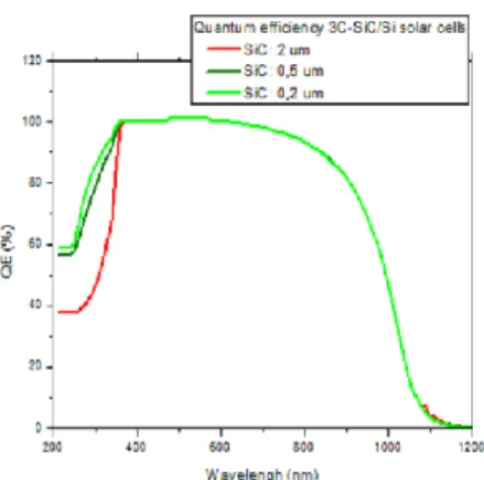
Figure 4: External quantum efficiency of the 3C-SiC/Si
As it can be seen on the graphs, the response is better in the ultraviolet between 200-400 nm for smaller emitter thickness. Moreover, in the higher wavelength range (L> 600 nm), an improvement in the response of the new cells compared to the former one diode is observed. This shows that the growth of SiC/Si has been improved since there is less degradation in the Si bulk. In addition, the metallization using Ti/Au, for the front contact, has made it possible to increase the performances in the cell’s efficiency according to the table 1.
C
onclusion
In order to improve the conversion efficiency of solar cells based on silicon carbide, a simple heterostructure has been studied. Simulations were performed, and then characterizations measured. The conclusion of this study shows that we obtain an improvement of the spectral response in the short wavelength domain thanks to the thinner layer of the emitter, then an improvement of the growth due to the non-degradation of electronic bulk properties in Si for wavelengths greater than 600 nm. The perspective of our work should consist of studying SiC-3C/Si tandem cells in order to better obtain a photovoltaic conversion of these cells in the short wavelengths.
Aknowledgements:
The authors thanks SCAC-Togo (Cultural Cooperation Service of the Embassy of France in Togo) and CRHEA for supporting this work.
Complementary informations on authors:
Kabe: [email protected]
Lare: [email protected], Lare Yendoubé researchgate.net
Ottaviani: [email protected], Laurent ottaviani researchgate.net
Pasquinelli: [email protected]
Barakel: [email protected]
Portail: [email protected]
REFERENCES1. Kefif K, Bouizem Y, Belfedal A, Sib JD, Benlakehal D, Chahed L. Hydrogen related crystallization in silicon carbide thin films. Optik. 2018;154:459–466.
2. Sprouster DJ, Koyanagi T, Dooryhee E, Ghose SK, Katoh Y, Ecker LE. Reprint of: Microstructural evolution of neutron irradiated 3C-SiC. Scr Mater. 15 janv 2018;143:176‑80.
3. Chung GS, Kim KS, Yakuphanoglu F. Electrical characterization of Au/3C-SiC/n-Si/Al Schottky junction. J Alloys Compd. oct 2010;507(2):508‑12.
4. Tanner P, Dimitrijev S, Harrison HB. Current mechanisms in n-SiC/p-Si heterojunctions. In: 2008 Conference on Optoelectronic and Microelectronic Materials and Devices. IEEE; 2008. p. 41–43.
5. Heidarzadeh H, Baghban H, Rasooli H, Dolatyari M, Rostami A. A new proposal for Si tandem solar cell: Significant efficiency enhancement in 3C–SiC/Si. Optik. 1 févr 2014;125(3):1292‑6.
6. Richards BS, Brown AS, Trupke T, Corkish RP, Green MA. β-SiC–based Photovoltaic and Optical Devices. In: Proceedings of ANZSES Conference. 2002.
7. Burgelman M, Verschraegen J, Degrave S, Nollet P. Modeling thin-film PV devices. Prog Photovolt Res Appl. 2004;12(2‑3):143–153.
8. Toure M, Berenguier B, Ottaviani L, Pasquinelli M, Palais O, Di Lauro P, et al. New 3C Silicon Carbide on Silicon Hetero-Junction Solar Cells for UV Collection enhancement. MRS Online Proc Libr Arch. 2014;1693.
9. Zielinski M, Portail M, Chassagne T, Juillaguet S, Peyre H. Nitrogen doping of 3C-SiC thin films grown by CVD in a resistively heated horizontal hot-wall reactor. J Cryst Growth. 2008;310(13):3174–3182.
10. Portail M, Zielinski M, Chassagne T, Chauveau H, Roy S, De Mierry P. Highly sensitive determination of N+ doping level in 3C–SiC and GaN epilayers by Fourier transform infrared spectroscopy. Mater Sci Eng B. 2009;165(1‑2):42–46.
Important: Articles are published under the responsability of authors, in particular concerning the respect of copyrights.
Readers are aware that the contents of published articles may involve hazardous experiments if reproduced; the reproduction of experimental procedures described in articles is under the responsability of readers and their own analysis of potential danger.
Reprint freely distributable – Open access article
Materials and Devices is an Open Access journal which publishes original, and peer-reviewed papers accessible only via internet, freely for all.
Your published article can be freely downloaded, and self archiving of your paper is allowed and encouraged!
We apply « the principles of transparency and best practice in scholarly publishing » as defined by the Committee on Publication Ethics (COPE), the Directory of Open Access Journals (DOAJ), and the Open Access Scholarly Publishers Organization (OASPA). The journal has thus been worked out in such a way as complying with the requirements issued by OASPA and DOAJ in order to apply to these organizations soon.
Copyright on any article in Materials and Devices is retained by the author(s) under the Creative Commons (Attribution-NonCommercial-NoDerivatives 4.0 International (CC BY-NC-ND 4.0)), which is favourable to authors.
Aims and Scope of the journal : the topics covered by the journal are wide, Materials and Devices aims at publishing papers on all aspects
related to materials (including experimental techniques and methods), and devices in a wide sense provided they integrate specific materials. Works in relation with sustainable development are welcome. The journal publishes several types of papers : A: regular papers, L : short papers, R : review papers, T : technical papers, Ur : Unexpected and « negative » results, Conf: conference papers.
(see details in the site of the journal: http://materialsanddevices.co-ac.com)
We want to maintain Materials and Devices Open Access and free of charge thanks to volunteerism, the journal is managed by scientists for science! You are welcome if you desire to join the team!
Advertising in our pages helps us! Companies selling scientific equipments and technologies are particularly relevant for ads in several places
to inform about their products (in article pages as below, journal site, published volumes pages, …). Corporate sponsorship is also welcome!