© EDP Sciences, Springer-Verlag 2013 DOI:10.1140/epjst/e2013-01916-x
T
HE
E
UROPEAN
P
HYSICAL
J
OURNAL
S
PECIALT
OPICS ReviewOn field effect studies and
superconductor-insulator transition in high-T
c
cuprates
G. Dubuis1,2, A.T. Bollinger1, D. Pavuna2, and I. Boˇzovi´c1
1 Condensed Matter Physics and Materials Science Department, Brookhaven National
Laboratory, Upton, NY 11973-5000, USA
2 Laboratory for Physics of Complex Matter, CREAM-ICMP–FSB, station 3, ´Ecole
Polytechnique F´ed´erale de Lausanne, 1015 Lausanne EPFL, Switzerland Received 18 March 2013 / Received in final form 12 May 2013 Published online 15 July 2013
Abstract. We summarize previous field effect studies in high-Tc
cuprates and then discuss our method to smoothly tune the carrier concentration of a cuprate film over a wide range using an applied electric field. We synthesized epitaxial one-unit-cell thick films of La2−xSrxCuO4 and from them fabricated electric double layer transis-tor devices utilizing various gate electrolytes. We were able to vary the carrier density by about 0.08 carriers per Cu atom, with the resulting change inTcof 30 K. The superconductor-insulator transition occurred at the critical resistance very close to the quantum resistance for pairs,RQ=h/(2e)2 = 6.5 kΩ. This is suggestive of a quantum phase transition, possibly driven by quantum phase fluctuations, between a “Bose insulator” and a high-Tc superconductor state.
1 Introduction
The carrier density plays a large role in determining the physical properties of corre-lated electron materials. For example, cuprates can be antiferromagnetic insulators, high critical temperature (Tc) superconductors, or ordinary metals, all within a small window of carrier concentrations. The electric field effect is thus a potentially valuable tool for the study of such materials [1]. Indeed, already back in 1988 Brazovskii and Yakovenko suggested the possibility to induce high-Tc superconductivity in La2CuO4
by the field effect [2]. The technical difficulty in implementing this idea was the rel-atively large carrier density required, of the order of 1021cm−3, which corresponds to an electronic screening length of≤1 nm. The latter in turn implies that one must secure an atomically smooth surface, which in the case of cuprates has been far from trivial. Nevertheless, the field effect has been demonstrated successfully in high-Tc
cuprates, following various approaches.
The familiar field effect transistor geometry uses a metallic top gate separated from the active film (“channel”) by a gate insulator. The latter must withstand the maximal electric field to be applied, and the leakage currents must be small. The lack of an adequate gate insulator turned out to be the key limiting factor in early studies of the electric field effect in cuprates that employed such FET geometry [3]. Namely,
to be able to induce the large desired changes in the carrier density, of the order of 1021cm−3, the breakdown field of the insulator must be larger than ∼108V/cm and such an insulator is not available.
An approach that proved more successful utilized an inverted metal-insulator-superconductor geometry, whereby the gate electrode was placed at the bottom of a SrTiO3 substrate, on top of which a high-TcYBa2Cu3O7−δ film was grown [4]. By applying a voltage to the back gate, the carrier density in the film was varied, producing Tc shifts of 10 K in Y1−yCayBa2Cu3O7−δ [5,6] and NdBa2Cu3O7−δ [7] films. The same technique of back gating SrTiO3 has also been used more recently to induce interface superconductivity, withTc = 310 mK, in the 2D electron gas at the LaAlO3-SrTiO3 interface [8].
The third approach is to use ferroelectric gating. In this arrangement, a layer of a ferroelectric material such as PbZrxTi1−xO3 is placed in between the superconduct-ing film and the gate electrode, and an applied gate voltage is used to change the polarization of the ferroelectric. In turn, this polarization field modulates the car-rier density, and thus the electronic properties, of the superconducting film. Shifts in Tc by several degrees Kelvin were induced in this way in GdBa2Cu3O7−δ [9] and NdBa2Cu3O7−δ [10].
Yet another design, the one that we adopted in our studies of the field-effect in cuprates, is the electric double layer transistor (EDLT). Here, voltage is applied be-tween a gate electrode and the channel material through a solid (polymer) or liquid electrolyte. Ions of one polarity are attracted to the gate electrode whereas ions of the opposite polarity are drawn to the channel, where an electronic double layer is formed at the electrolyte-channel interface. Within the double layer, electric field is very high it can exceed 108V/cm. Using polymer electrolytes (salts dissolved in a polymer such as polyethylene glycol), two-dimensional carrier density as high as 1014cm−2has been achieved. Even higher densities of∼8 × 1014cm−2 have been attained using ionic liq-uids (molten organic salts) as the electrolyte. This is comparable to the carrier density of high-Tc cuprates, and hence EDLT technique offers new opportunities for
study-ing the field effect in these materials. Indeed, already from early nineties, McDevitt and collaborators applied EDLT technique to YBa2Cu3O7−δ, Tl2Ba2CaCu2O8 and Tl2Ba2Ca2Cu3O10 and demonstrated spectacularly large shifts of Tc [11–15]. Using the same technique in recent years, Iwasa, Kawasaki, and collaborators were able to induce superconductivity by the field effect in an insulator (SrTiO3) [16] as well as a semiconductor (ZrNCl) [17]. They have also demonstrated, for the first time, su-perconductivity in KTaO3 [18]. While admittedly the Tc was quite low (∼0.05 K), nevertheless this was a seminal result, since this was the first new superconductor discovered by the electric field effect techniques.
2 Experimental results
In the last several years, we have extensively used the EDLT technique to study the basic physics of high-Tc superconductivity (HTS) in cuprates. In particularly, we were interested in the superconductor-insulator transition (SIT) that occurs in La2−xSrxCuO4(LSCO) as the doping is tuned around the critical value ofxc≈ 0.06. Indeed, we were driven by the prospects to reversibly and at will display the wealth of cuprate physics in a single sample by applying an electric field. The traditional ap-proach to studying a particular segment of the cuprate phase diagram is to synthesize many individual crystals or thin films with different levels of doping. This is generally not only very time and labor intensive, but also subject to large uncertainty in the actual stoichiometry and doping levels. Moreover, chemical doping also induces dis-order due to random distribution of dopant atoms. In contrast, the principal effect of
Fig. 1. Illustration of our electrolyte double-layer transistor and the Hall-Effect bar device, which is immersed in electrolyte. The gate voltage is applied by a Pt counter-electrode, or a coplanar Au electrode through the electrolyte [22].
the electrostatic technique described here is just to modify the carrier density in the films. Consequently, the EDLT technique not only allows one to study the intrinsic properties of cuprates, but also to determine the relative contributions of electronic doping and disorder to phenomena such as quantum phase transitions.
For EDLT studies, we synthesized ultrathin one- unit-cell (1 UC) or two-unit-cell (2 UC) thick LSCO films using atomic-layer-by-layer molecular beam epitaxy [19]. This technique allows reproducible fabrication of atomically smooth films of cuprates with control over the stoichiometry at the 1% level. We have demonstrated the capa-bility to synthesize films in which HTS superfluid is confined to a single CuO2plane, and yet the critical temperature is comparable to that in optimally doped bulk LSCO single crystals [20–22]. The films thickness is controlled digitally, in real time, using reflection high-energy electron diffraction which shows pronounced oscillation with the period corresponding to assembly and completion of exactly one molecular layer on the surface.
Subsequently, we pattern the films using photolithography to form Hall-effect de-vices (see Fig.1). We study them by sequences of automated resistance measurements while thermally cycling the samples from room temperature to 4 K. In one thermal cycle, at a chosen temperature we apply the desired gate voltage to our devices, charge them for a selected time, and subsequently measure the resistance as a function of temperature (at a constant cooling rate).
Initially, we have chosen to use the ionic liquid DEME-TFSI as a gate electrolyte, as it had been successfully used by other researchers in this field [11–18]. Other electrolytes we tested included the solution of NaF in polyethylene glycol, as well as the ionic liquid C6MIm-BF4. For each of these electrolytes, we studied in detail the charging characteristics of our devices at different temperatures.
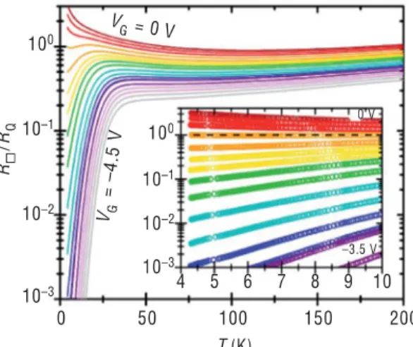
Using this approach, we were able to apply very large electric fields on 1 UC or 2 UC thick LSCO films. We induced large changes in the surface carrier den-sity, up to about 0.08 carriers per Cu atom, that caused Tc to shift by up to 30 K. Hundreds of resistance vs. temperature and carrier density curves were recorded by virtue of the automation described above. This allowed us to study the physics of the superconductor–insulator transition (SIT) in monolayer LSCO films (see Fig. 2) in great detail. We were able to determine the critical sheet resistance in several devices on different films, and it turned to be quite close to the quantum resistance for pairs, RQ = 6.5 kΩ. The scaling analysis allowed us to determine the product of the critical
exponents. The results were consistent with a 2D quantum phase transition driven by quantum phase fluctuations, between HTS state and a “Bose insulator” state with localized pairs [23–25]. Indeed, in a recent review [26], we have shown that in several
Fig. 2. Superconductor–insulator transition driven by electric field. Temperature depen-dence of normalized resistance of an initially heavily underdoped and insulating film. The device (see Fig.1) employs a coplanar Au gate and DEME-TFSI ionic liquid. The carrier density, fixed for each curve, is tuned by varying the gate voltage from 0 V to −4.5 V in 0.25 V steps; an insulating film becomes superconducting via a quantum phase transition. The inset highlights the separatrix independent of temperature in the range from 4 K to 10 K. The open circles are the actual raw data points; the black dashed line is quantum resistance for pairs; the critical sheet resistance is equal to the quantum resistance of pairs, RQ=h/4e2= 6.5 kΩ [15].
otherp-type cuprates, SIT also occurs at the critical sheet resistance approximately equal to the pair quantum resistance.
More recently, the groups of Allen Goldman at University of Minnesota as well as the IWASA group reported several further studies of cuprates, both YBa2Cu3O7−δ and La2CuO4, by EDLT technique [27–30]. While most findings are broadly consistent with ours, clearly much more work needs to be done, ideally extended to additional quasi-2D materials and to much lower temperatures.
I.B. and A.T.B. were supported by the US Department of Energy, Basic Energy Sciences, Materials Sciences and Engineering Division. G.D. and D.P. were supported by the Labora-tory for Physics of Complex Matter-EPFL, and the Swiss National Science Foundation.
References
1. C.H. Ahn, J.-M. Triscone, J. Mannhart, Nature 424, 1015 (2003) 2. S.A. Brazovskii, V.M. Yakovenko, Phys. Lett. A 132, 290 (1988)
3. A. Cassinese, G.M. De Luca, A. Prigiobbo, M. Salluzzo, R. Vaglio, Appl. Phys. Lett. 84, 3933 (2004)
4. J. Mannhart, J.G. Bednorz, K.A. Mueller, D.G. Schlom, Z. Phys. B Cond. Matter 83, 307 (1991)
5. G.Yu. Logvenov, A. Sawa, C.W. Schneider, J. Mannhart, Appl. Phys. Lett. 83, 3528 (2003)
6. G.Yu. Logvenov, C.W. Schneider, J. Mannhart, Yu.S. Barash, Appl. Phys. Lett. 86, 202505 (2005)
7. D. Matthey, N. Reyren, J.-M. Triscone, T. Schneider, Phys. Rev. Lett. 98, 057002 (2007) 8. A.D. Caviglia, S. Gariglio, N. Reyren, D. Jaccard, T. Schneider, M. Gabay, S. Thiel,
9. C.H. Ahn, S. Gariglio, P. Paruch, T. Tybell, L. Antognazza, J.-M. Triscone, Science 284, 1152 (1999)
10. S. Gariglio, C.H. Ahn, D. Matthey, J.-M. Triscone, Phys. Rev. Lett. 88, 067002 (2002) 11. S.R. Peck, L.S. Curtin, J.T. McDevitt, R.W. Murray, J.P. Collman, W.A. Little, T. Zetterer, H.M. Duan, C. Dong, A.M. Hermann, J. Amer. Chem. Soc. 114, 6771 (1992)
12. S.G. Haupt, D.R. Riley, J.T. Mcdevitt, Adv. Mater. 5, 755 (1993)
13. S.G. Haupt, D.R. Riley, J. Zhao, J.-P. Zhou, J.H. Grassi, J.T. Mcdevitt, Proc. SPIE. 2158, 238 (1994)
14. S.G. Haupt, D.R. Riley, J.H. Grassi, R.K. Lo, J. Zhao, J.-P. Zhou, J.T. Mcdevitt, J. Amer. Chem. Soc. 116, 9979 (1994)
15. M.B. Clevenger, C.E. Jones, S.G. Haupt, J.N. Zhao, J.T. Mcdevitt, Proc. SPIE 2697, 508 (1996)
16. K. Ueno, S. Nakamura, H. Shimotani, A. Ohtomo, N. Kimura, T. Nojima, H. Aoki, Y. Iwasa, M. Kawasaki, Nat. Mater. 7, 855 (2008)
17. J.T. Ye, S. Inoue, K. Kobayashi, Y. Kasahara, H.T. Yuan, H. Shimotani, Y. Iwasa, Nat. Mater. 9, 125 (2010)
18. K. Ueno, S. Nakamura, H. Shimotani, H.T. Yuan, N. Kimura, T. Nojima, H. Aoki, Y. Iwasa, M. Kawasaki, Nature Nanotechnol. 6, 408 (2011)
19. I. Bozovic, IEEE Trans. Appl. Superconductivity 11, 2686 (2001)
20. A. Gozar, G. Logvenov, L. Fitting Kourkoutis, A.T. Bollinger, L.A. Giannuzzi, D.A. Muller, I. Bozovic, Nature 455, 782 (2008)
21. G. Logvenov, A. Gozar, I. Bozovic, Science 326, 699 (2009)
22. A.T. Bollinger, G. Dubuis, J. Yoon, D. Pavuna, J. Misewich, I. Bozovic, Nature 472, 458 (2011)
23. M.P.A. Fischer, G. Grinstein, S.M. Girvin, Phys. Rev. Lett. 64, 587 (1990) 24. A.M. Goldman, N. Markovi´c, Physics Today 51, 39 (1998)
25. V.F. Gantmakher, V.T. Dolgopolov, Physics – Uspekhi 53, 1 (2010)
26. G. Dubuis, A. Bollinger, D. Pavuna, I. Bozovic, J. Superc. Nov. Magn. 26, 749 (2013) 27. X. Leng, J. Garcia-Barriocanal, S. Bose, Y. Lee, A.M. Goldman, Phys. Rev. Lett. 107,
027001 (2011)
28. T. Nojima, H. Tada, S. Nakamura, N. Kobayashi, H. Shimotani, Y. Iwasa, Phys. Rev. B 84, 020502(R) (2011)
29. X. Leng, J. Garcia-Barriocanal, B. Yang, Y. Lee, J. Kinney, A.M. Goldman, Phys. Rev. Lett. 108, 067004 (2012)
30. J. Garcia-Barriocanal, A. Kobrinskii, X. Leng, J. Kinney, B. Yang, S. Snyder, A.M. Goldman, Phys. Rev. B 87, 024509 (2013)