HAL Id: hal-01910144
https://hal.archives-ouvertes.fr/hal-01910144
Submitted on 31 Oct 2018HAL is a multi-disciplinary open access archive for the deposit and dissemination of sci-entific research documents, whether they are pub-lished or not. The documents may come from teaching and research institutions in France or abroad, or from public or private research centers.
L’archive ouverte pluridisciplinaire HAL, est destinée au dépôt et à la diffusion de documents scientifiques de niveau recherche, publiés ou non, émanant des établissements d’enseignement et de recherche français ou étrangers, des laboratoires publics ou privés.
MEMS Four-Terminal Variable Capacitor for low power
Capacitive Adiabatic Logic with High Logic State
Differentiation
Hatem Samaali, Y. Perrin, A. Galisultanov, H. Fanet, Gaël Pillonnet, Philippe
Basset
To cite this version:
Hatem Samaali, Y. Perrin, A. Galisultanov, H. Fanet, Gaël Pillonnet, et al.. MEMS Four-Terminal Variable Capacitor for low power Capacitive Adiabatic Logic with High Logic State Differentiation. Nano Energy, Elsevier, 2018, �10.1016/j.nanoen.2018.10.059�. �hal-01910144�
MEMS Four‐Terminal Variable Capacitor
for low power Capacitive Adiabatic Logic
with High Logic State Differentiation
H. Samaali1, Y. Perrin2, A. Galisultanov2, H. Fanet2, G. Pillonnet2*, P. Basset1* 1 Université Paris-Est, ESYCOM, ESIEE Paris, Noisy-le-Grand 93160, France
2 Université Grenoble Alpes, CEA, LETI, F-38000 Grenoble, France * Contact authors: [email protected], [email protected]
Abstract
This paper presents a novel four-terminal variable capacitor (FTVC) dedicated to the recent concept of low power capacitive adiabatic logic (CAL). This FTVC is based on silicon nano/micro technologies and is intended to achieve adiabatic logic functions with a better efficiency that by using field effect transistor (FET). The proposed FTVC consists of two capacitors mechanically coupled and electrically isolated, where a comb-drive input capacitor controls a gap-closing capacitor at the output. To fully implement the adiabatic combinational logic, we propose two types of variable capacitors: a positive variable capacitor (PVC) where the output capacitance value increases with the input voltage, and a negative variable capacitance (NVC) where the output capacitance value decreases when the input voltage increases. A compact and accurate electromechanical model has been developed. The electromechanical simulations demonstrate the ability of the proposed FTVC devices for CAL, with improved features such as high logic states differentiation larger than 50% of the full-scale input signal and cascability of both buffers and inverters. Based on the presented analysis, 89% of the total injected energy in the device can be recovered, the remaining energy being dissipated through mechanical damping. During one cycle of operation, a buffer gate of 10x2.5 µm2 dissipates only 0.9 fJ.
Keywords: Capacitive Adiabatic Logic, Ultra low power circuits, M/NEMS, Capacitive
logic gates, Four Terminal Variable Capacitor (FTCV)
1. Introduction
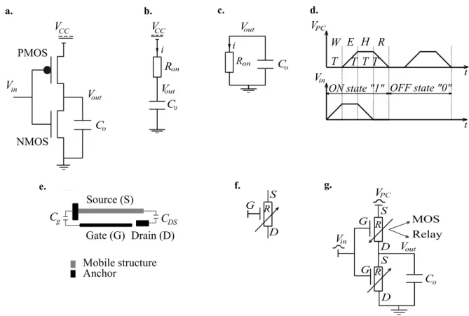
A digital electronic circuit can be considered as a chain of interconnected elementary blocks [1], each of them having an input capacitance Co corresponding to the gate capacitor of
a field effect transistor (FET) and some parasitic interconnections. In current CMOS technology, the classical combinational logic is based on the abrupt charge and discharge of Co through PMOS and NMOS transistors for coding a logic state, as in the CMOS inverter
(Figure 1a). When changing from “0” to “1” logic state (Vin 0), Co is charged from the
power supply VCC through the PMOS resistance in on-state Ron, while the NMOS is in its
cut-off region (Figure 1b). During this operation, the energy provided by the source is given by QVCC = CoVCC2: half of it is dissipated through Ron and the other half is stored in Co. When
changing from “1” to “0” (Vin 1), Co is now discharged to the ground through the NMOS
transistor in ON state (Figure 1c). The energy previously stored in Co is now dissipated into
the ground and the total energy provided by the source is eventually fully dissipated.
In addition to the active power dissipation CoVCC2f, where f is the operating frequency,
there are dissipation due to the short-circuit transition and the sub-threshold leakage IleakVCC,
where Ileak is the sub-threshold leakage current. The short-circuit transition power corresponds
to about 10% of the average power and is typically the smallest contribution to the losses [3] [4][5]. Though among all VLSI logic families, CMOS circuits have the lowest power dissipation [2][3], reducing the energy consumption is one of the main concerns in modern integrated circuits (IC). It can be reduced by (i) developing devices with higher sub-threshold slope, (ii) reducing Co and (iii) working at low frequency. Reducing Co is limited by the
lithography. Reducing the supply voltage VCC is a powerful method but this solution has
limits related to the transistor size reduction [6]. Consequently, the dissipation cannot be reduced significantly.
In the early sixties, Landauer stated that to erase one bit of known information, which is consider as the most basic computing event, it requires the dissipation of at least kB.T.ln(2),
where kB is the Boltzman constant and T is the temperature in Kelvin [7]. At room
temperature, it corresponds to 18 meV. However, to overcome the energy barrier due to the thermal noise, a minimum of 100.kB.T (~2.6 eV at 300°K) is required [8]. As a comparison,
the current dissipated energy at each switching event, with the 10 nm CMOS technology, is given by 0.5C0Vcc² ~40 eV, which is about 3 orders of magnitude above the Landauer limit
and one order of magnitude above the thermal noise limit.
A good way to even further reduce the power consumption is the adiabatic logic approach [6][9], which can be combined with the concept of “energy recovery” [10]. It consists in charging the gate capacitor with a constant current, instead of a constant voltage as in classical digital circuits, then to recover the injected charge when going back to the initial state. It results in an optimized power dissipation [11] but requires a dynamic logic: the charge and discharge of Co have to be performed by a ramped supply voltage signal VPC called
the Power Clock (PC).
a) Dissipated energy in CMOS adiabatic logic
The principle of the adiabatic logic is detailed in [6][9]. To explain the principle of operation of an adiabatic logic gate, let us consider the schematic of the inverter gate in Figure 1a. The PC signal is typically divided into 4 equal steps of equal duration T, that we named the Evaluate (E), Hold (H), Recovery (R) and Wait (W) intervals. Consequently, a logic “1” state at the input voltage Vin is not a DC voltage value anymore as well. It corresponds to the
power clock signal but shifted by a quarter of period T, as shown in Figure 1d.
During the charging phase (Evaluate stage), the supply voltage is ramped from 0 to VCC
within the charging time T, and the current i is determined by:
The energy dissipated through Ron during the charging and discharging phases is then given
by:
0 𝐸 2𝑖 𝑅 𝑇 2 𝑅 𝑇 2 𝐶 𝑉
If the time constant 2RonCo is lower than T, the energy dissipation is reduced compared to the
energy dissipation CoVCC2 in classical CMOS circuits. The ramp duration of the PC (also
equal to T) strongly affects the Joule dissipation: Edynamic vanishes for long charging times.
Similarly, scaling down the supply voltage and reducing the capacitance load also reduce the dissipated energy in adiabatic logic, as we mentioned earlier.
In addition, it exits a non-adiabatic energy associated to the incompressible threshold voltage 𝑉 of the MOS transistor equal to:
0 𝐸 𝐶 𝑉 ,
And a leakage current can flow from the supply voltage to the ground through the disable transistors due to the semiconductor technology, leading to a static energy dissipation given by:
0 𝐸
where 𝐼 is the mean leakage current.
By taking into account the (adiabatic) dynamic losses, the (static) leakage and the (uncompressible) non-adiabatic losses, we can express the total energy dissipation of an adiabatic inverter gate based on CMOS transistors as:
0 𝐸 2 𝐶 𝑉 𝐶 𝑉 𝐼 𝑉
b) Electromechanical devices to reduce the non‐adiabatic losses
Nano-Electromechanical relays (NEMS relays) have been proposed to replace CMOS transistors in order to reduce the static and non-adiabatic losses. Most of them are electrostatically actuated [12][13] but a nanomagnetic switch could also be used [8]. These nanorelays need low switching energy and promise perfect isolation with zero leakage current in the OFF state. They have already been evaluated for classical logic [14]-[15] and even tested with an integrated circuit [16]. In addition, they can be used efficiently for the adiabatic logic [17].
A classical NEMS relay has typically three terminals, the gate (G), the source (S) and the drain (D) (Figure 1e). It consists in an electrostatic actuator made of a flexible beam S and a fixed electrode G, forming a variable capacitance Cg (Figure 1e). The voltage across Cg
determines the state of the relay. In the OFF state, Cg is low and the resistance R between the
drain and the source is infinite (open circuit). When an input voltage is applied between S and G, the beam deflects and creates a resistive contact between the drain and the source (ON
states). Consequently, the relay can be seen as a capacitor controlling a variable resistor, represented with the symbol in Figure 1f. To implement all combinational logic, we need two types of relay: normally-ON and normally-OFF relays to replace the NMOS and PMOS transistors in integrated circuits respectively. Figure 1gillustrates how the relays (or the MOS transistors) can be implemented in an adiabatic inverter.
Figure 1. From classical CMOS inverter to inverter based on adiabatic logic. a) Schematic of a
conventional CMOS inverter. b) Equivalent circuit in charging phase. c) Equivalent circuit in discharging phase. d) PC circuit signals. e) Implementation of a resistive electromechanical relay and f) its schematic representation. g) Schematics of an adiabatic resistive inverter.
However, the unavoidable contact resistance of resistive micro/nano-electromechanical relays, their poor mechanical reliability and their low switching frequencies have been highlighted in literature [12]-[17]. In order to avoid the resistive contact in the on-state and to reduce the dynamic dissipation, a purely capacitive electromechanical switch could be a better solution [18]. Based on this new paradigm, the so-called Capacitive Adiabatic Logic (CAL), Galisultanov et al have detailed in [19] the concept of a fully contact-less electromechanical device for the CAL. In this paper we described new four-terminal variable capacitors (FTVC) for the CAL that still have a contact zone but present several major advantages, like a better differentiation between a “0” and a “1” logic state, a higher frequency of operation or a smaller area. In addition, based on our simulations, we demonstrated for the first time the ability to cascade several devices.
The organization of the paper is as follows. In the next section, we detail these new FTVC and their mathematical models that can be used to implement the CAL approach. In section 3, we analyze the different energy losses of the proposed configurations. We conclude with the demonstration of the operation of cascaded elementary combinational gates.
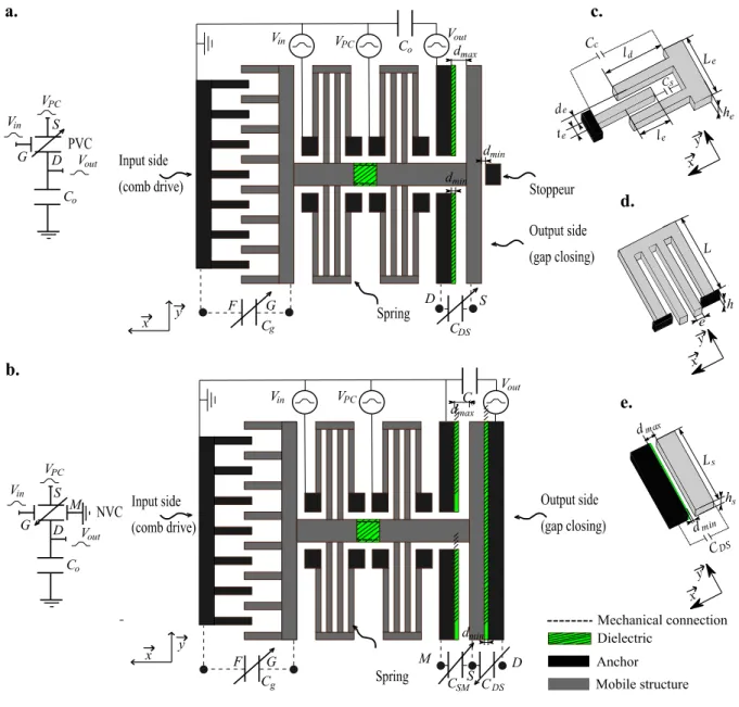
Figure 2. Electromechanical implementations of FTVC in the OFF state. a) Electromechanical
implementation of a buffer with a PVC. b) Implementation of an inverter with a NVC. c) Geometric details for the comb-drive capacitance Cg for ne=1. d) Geometric details for a spring. e) Geometric details for the gap-closing capacitance CDS.
2. Proposed architectures for the CAL devices
a) General description
In the Capacitive Adiabatic Logic approach, the resistive elements (transistors or relays) are replaced by purely capacitive elements. Similarly to the resistive-based adiabatic logic, the
logic function required an input capacitance Cg between the gate G and the ground, and an
output capacitance CDS between the terminals D and S (we use the FET transistor notation, i.e.
the input voltage Vin is applied between the gate and the ground). The only difference is that
the electrodes of CDS are never in ohmic contact. All the terminals are electrically isolated, but
two of them (G and S) are mechanically connected. Two types of output variable capacitances are needed to fully implement the adiabatic combinational logic: Positive Variable Capacitances (PVC) where CDS increases with the control voltage Vin and Negative Variable
Capacitances (NVC) where CDS decreases when Vin increases.
In the following, we propose implementations for a PVC and a NVC that can be fabricated in silicon micro/nanotechnologies. Each device consists of an electrostatic comb-drive actuator for the input capacitance Cg and a gap-closing (possibly with interdigited-combs) for
the output capacitor CDS. The capacitance Cg and CDS are mechanically connected but
electrically separated by a dielectric. Figure 2a shows a schematic top-view of a practical buffer using a PVC and Figure 2b depicts an inverter with a NVC, both in the OFF state.
Figure 2c,d,e give more geometric details of Cg, the spring mechanical suspensions and CDS
respectively.
b) Principle of the PVC configuration
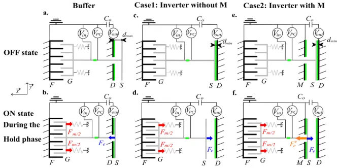
Let’s assume that the buffer in Figure 2a is loaded with the signals presented in Figure 1d. In the OFF state (Vin=0), the electrodes S and D are separated by dmax, and the capacitance CDS
is minimum (Figure 3a). When Vin is applied (ON state), the comb-drive moves the rotor in
the 𝑥⃗ direction, resulting in an increase of Cg and CDS. According to the capacitor divider {Co
-CDS}, the output Vout follows VPC. The electrical force Fe, created by the voltage VDS=VPC-Vout,
is opposed to the mechanical spring force Fm (Figure 3b). Consequently, during the Hold
interval when Vin decreases, Fe balances Fm and the equilibrium is maintained: Cg and CDS
remain constant, allowing Vout to still follow VPC.
c) Principle of the NVC configuration
Now we consider the inverter in Figure 2b loaded with the same signals in Figure 1d. In the OFF state (Vin=0), CDS is maximal because S and D are separated by dmin, the thickness of
a dielectric layer covering the electrodes (Figure 3c). When Vin is applied (ON state), the
comb-drive moves the rotor in the 𝑥⃗ direction, resulting in an increase of Cg and a decrease of
CDS. This time, the electrical force Fe and spring force Fm are in the same direction (Figure 3d). Consequenctly, during the Hold interval when Vin decreases, the mobile electrode may
return to its initial position causing an incorrect operation. To avoid this problem, we proposed to add an additional electrode M connected to the ground and forming with S a capacitance CSM. The voltage across CSM creates an additional electrical force Fe’ that
Figure 3. Different states of the buffer (PVC) and the inverter (NVC). a) Buffer in the OFF state. b). Buffer in the ON state during the Hold phase. c) Inverter without M in OFF state. d) Inverter without M in the ON state during the Hold phase. e) Inverter with M in OFF state. f) Inverter with M in the ON state during the Hold phase.
d) The adiabatic conditions
Conditions related to input signals
In order to satisfy the adiabatic conditions, the inputs have to be stable during ramp-up and ramp-down phases of the PC, and the durations of the Evaluate, Hold, and Wait phases of both input and power-clock signals have to be equal [20][21]. Therefore, as already stated in the introduction, a four-phase power clock consisting in four equal intervals T is required, and the input signal is shifted by a quarter of period with respect to the PC. In the ON state, the following rules have to be followed :
(i) During the Wait interval, Vin ramps up, Cg increases and reaches its maximum value
at the end of the interval. As soon as Cg increases, CDS evolves depending on the
gate configuration: for a PVC, it increases until its maximum and for the NVC, it decreases to its lower value.
(ii) During the Evaluate interval, VPC increases and Vin remains constant at its high
value. In the PVC configuration, the output Vout follows the PC and the capacitance
node Co starts to charge. In the NVC, the output remains at a low level.
(iii) During the Hold interval, Vin decreases but VPC remains high, and then the variables
capacitances Cg and CDS doesn’t change (thanks to the help of electrode M for the
NVC).
(iv) During the Recover interval, VPC decreases while Vin remains grounded. The
mechanical equilibrium is holded until low value of VPC, thanks to the typical
hysteresis in electrostatic transducers [23]. Both Cg and CDS remain constant till
To build a circuit, the CALs gates are cascaded and each gate is supplied by a PC, as shown in Figure S1. Since the output signal follows the PC, two subsequent PC should be delayed by a quarter of period to satisfy the adiabatic conditions. Therefore, a four-phase power-clock (VPC1 to VPC4) is needed to cascade several gates.
Conditions related to CDS
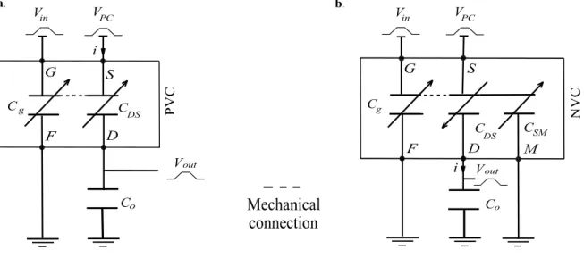
Figure 4 shows schematic representations of a buffer and an inverter. The PVC design has four terminals while NVC has five, since it includes the additional electrode M. The electrical equations are given by:
0 𝑉 𝑉 𝑉
0 𝑖 𝐶 𝑉 𝐶
where VDS, Co, and i are the voltage across the drain and source of either PVC or NVC, the
input capacitance of the following gate and the current provided by the power clock respectively. We can deduce the instantaneous logic output voltage as:
0 𝑉 𝑉 𝐶
𝐶 𝐶
Since the input voltage Vin controls the value of CDS, it also controls the voltage ratio between
the power-clock signal and the output node through the capacitor bridge divider {CDS-Co}.
The values of CDS have to be carefully chosen: the minimum value of CDS has to be small
compared to Co in order to obtain the low logic state, and the maximum value of CDS has to be
high compared to Co to achieve the high logic level.
e) Modelling the CAL devices
Modeling the input capacitance variation
Various models can be found in the literature to model capacitances and their fringe fields. In this work, we use the Mejis-Fokkema formula [22] for the comb-drive Cg and the Palmer
formula [24] for the gap-closing capacitances CDS and CSM.
For Cg 0, the first term Cc represents the lateral capacitance without fringing effect, Cf
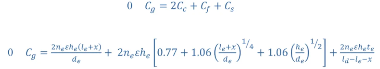
estimates the fringe capacitance and Cs is the capacitance at the tip of fingers (c.f. Figure 2c): 0 𝐶 2𝐶 𝐶 𝐶
0 𝐶 2𝑛 𝜀ℎ 0.77 1.06 1.06
where ne and he represents the comb’s finger numbers and their thickness respectively. le, de,
ld and te are the initial overlapping distance between the fingers, the initial gap distance
between the fixed and movable fingers, the length and width of the finger respectively. 𝜀 is the air permittivity and 𝑥 is the displacement in the 𝑥⃗ direction. This model is in good agreement with the commercial software MEMS+ from Coventorware (cf Figure S2)
Modeling the ouput capacitance variation
The gap-closing capacitance CDS is given by the Palmer formula [24], 0 and 0 for PVC and
NVC respectively:
0 𝐶 1 2 1 log
0 𝐶 1 2 1 log
The expression of CSM is similar to the expression of CDS in PVC, and is expressed by:
0 𝐶 𝐶 𝑛 ℎ 𝐿 𝜀 𝑑 𝑥 1 2 𝑑 𝑥 ℎ 𝜋 1 log ℎ 𝜋 𝑑 𝑥
where ns, hs, Ls , dmax or dmin are the number of CDS electrodes, their thickness, their length and
their initial gap distance respectively.
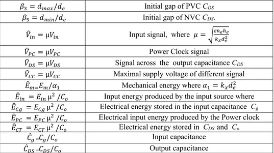
Table 1. Non-dimensional variables
Variable Description
𝑥 𝑥 𝑑⁄ Displacement in the direction 𝑥⃗
𝑡̂ 𝑡 𝑘 /𝑚 Time
𝜆 𝑐/ 𝑚. 𝑘 Damping
𝛽 𝑙 𝑙 /𝑑 Gap of the side capacitance Cs 𝛽 𝑙 /𝑑 Overlapping distance between fingers
𝛽 𝑑 /𝑑 Initial gap of PVC CDS 𝛽 𝑑 /𝑑 Initial gap of NVC CDS.
𝑉 µ𝑉 Input signal, where 𝜇 𝑉 µ𝑉 Power Clock signal
𝑉 µ𝑉 Signal across the output capacitance CDS 𝑉 µ𝑉 Maximal supply voltage of different signal 𝐸 𝐸 /𝛼 Mechanical energy where 𝛼 𝑘 𝑑 𝐸 𝐸 µ /𝐶 Input energy produced by the input source where 𝐸 𝐸 µ /𝐶 Electrical energy stored in the input capacitance Cg 𝐸 𝐸 µ /𝐶 Electrical input energy produced by the Power clock 𝐸 𝐸 µ /𝐶 Electrical energy stored in CDS and Co
𝐶 =𝐶 /𝐶 Input capacitance 𝐶 =𝐶 /𝐶 Output capacitance
Table 2. Physical and geometric parameters used in simulations.
Variable Description Value
E Yong’s modulus of silicon (N/m2) 169 109 ε Permittivity of air (F/m3) 8.854 10-12 Ls Length of the gap closing capacitance CDS (µm) 8.72 hs Thickness of the gap closing capacitance CDS (µm) 0.4 he Thickness of the comb-drive capacitance Cg (µm) 0.4 dmax Initial gap distance of CDS (µm) 0.25 dmin Thickness of the dielectric (µm) 0.01 ns Number of the gap-closing capacitance CDS 1
ne Number of finger in Cg 55
L Length of the mechanical suspension (µm) 5 e Width of mechanical suspension (µm) 0.02 h Thickness of mechanical suspension (µm) 0.4 Le Length of the comb-drive capacitance Cg (µm) 8.8 de Gap distance of the comb-drive capacitance Cg(µm) 0.04 te Width of the finger of the comb-drive capacitance Cg (µm) 0.04 le Overlapping distance between fingers of Cg (µm) 0.02 ld Length of the finger of the comb-drive capacitance Cg (µm) 0.4 m Effective mass of the movable part (Kg) 1.98 10-14 Kx Spring constant in the direction 𝑥⃗(N/m) 0.02
c Damping (Kg/s) 1.96 10-8
Co Load capacitance (fF) 1
Modeling the device dynamics
From the Newton’s second law, the dynamic behavior of the PVC and NVC structures is represented by the non-dimensional equation 0. The first term is associated to the kinetic force, the second term is associated to the mechanical damping force, the third one is related to the spring force, the fourth one represents the electrical force from Cg and the next one is
the electrical force from CDS. The last term represents the electrical force associated to CSM for
0 𝑥 𝜆𝑥 𝑥 𝑉 1 . 𝛼 𝛼 𝑉 1 𝛽 𝛽 𝑥
𝛽 𝑥 𝛼 𝑉
1 𝛽 𝛽 𝑥
𝛽 𝑥 0
where 𝛾 0.265, 𝛽 , 𝛼 , 𝛼 1 and 𝛼 0, for PVC configuration and 𝛼 𝛼 1 for NVC.
Modeling the impact
At each impact between the drain and the source electrodes, the mobile electrode losses a small part of its kinetic energy during a bouncing phenomenon. During successive contacts, the velocity can be expressed as [25][26]:
0 𝑥 𝐾 𝑥
where 𝑥 and 𝑥 are the velocities before and after the 𝑛 impact, and Kloss is the
coefficient of restitution. When the mobile electrode reaches the contact, its velocity is set according to 0. The characteristics of the bounces depend on the mass of the mobile part and its velocity, the elastic response of the material and the surface hardness [26].
3. Simulations and analysis
In this section, we present and analyze the simulations of Capacitive Adiabatic Logic circuits using the MEMS devices presented previously. The physical and geometrical features of the proposed implementations are given in Table 2. These dimensions are carefully chosen in order to match the FET transistor parameters. First, we present how a buffer or an inverter works. Then we study the energy transfer and losses in a buffer gate. Finally, we demonstrate the possibility to cascade in series several buffers or inverters.
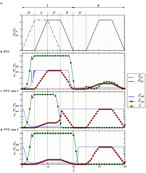
In the following, a “1” adiabatic logic input (i.e. the “ON state”) corresponds to a 4-interval pulse similar to VPC, but with a phase shift of a quarter of period in order to satisfy the
adiabatic logic conditions. A “0” (“OFF state”) means Vin=0 during the entire sequence
Figure 5. Operation of simple gates for a “1 0” logic input. a) the input and PC signals. b) Simulation of a CAL buffer. c) Simulation of a CAL inverter without electrode M (case 1) and d) with electrode M (case 2). All dimensions are given in Table 1.
a) Analysis of a single gate
Simulation of a buffer
In order to understand how a CAL buffer works, we plotted in Figure 5b the output voltage of a PVC and the displacement of its mobile part for the input logic sequence “1 0” shown in
Figure 5a. Co is set to 1 fF according to [1]. During the “1” state, as soon as Vin increases
(Wait interval), the comb-drive at the input moves the mobile part, ds=dmax-x decreases and
CDS increases from its minimum to its maximum value, with a short oscillation induced by the
impact of the mobile mass onto the rigid frame. Then, during the Evaluate interval, Vin, and so
CDS are constant, while VPC increases. CDS is at its maximum value and Vout follows VPC
through the constant capacitive divider formed by the {CDS-Co} couple. This lasts even
beyond the Hold interval, while Vin decreases till 0V, because of the electrostatic force Fe
across CDS introduced by VPC is still higher than the restoring force of the mechanical springs
important to keep CDS at its maximum value, allowing Vout to follow the PC. During the
Recovery interval, Vout progressively decreases with VPC, and at some point the electrostatic
force associated to CDS is not sufficient to compensate the restoring spring force, so CDS
rapidly decreases to its minimum value, bringing Vout definitely to 0V.
Then the “0” state starts. Vin remains equal to 0 during the 4 intervals of VPC and the
electrostatic force across Cg is null. However, when VPC increases during the Evaluate
interval, its associated electrostatic force leads to a small variation of CDS that is not negligible
compare to Co, so we can observe a small variation of Vout following the evolution of VPC. In
addition, we can also observe a tiny increase of CDS due to the electrostatic force across CDS
introduced by VPC. However Vout has to remain below the threshold voltage corresponding to
the “0” logic state.
Simulation of an inverter
Similarly, the time history of a NVC loaded with a capacitor Co of 1 fF is given in Figure 5c and d for the same “ 1 0” logic input. At t=0, CDS is at its maximum and Vin starts to
increase from 0 V to VCC (Wait interval). Vout is initially equal to 0V, so the mobile electrode
easily moves with the increase of Vin, and CDS quickly decreases to its minimum value.
During the Evaluate interval, Vin and so CDS remain constant. Since VPC increases and CDS is
not negligible, Vout follows VPC but has to remain below the maximum voltage allowed for a
“0” logic level. During the following Hold interval, Vin decreases. First CDS remains at its
minimum because the electrostatic force across Cg is still higher that the spring restoring
force. However, at some point, this is not the case anymore. Then CDS increases, while VPC is
still high, which leads to an unexpected increase of Vout before the next “0” logic at the input
(case 1 Figure 5c). To avoid this, we added the M electrode connected to the ground that creates an additional electrostatic force across CSM, controlled by VPC and opposed to the
spring force (Figure 3e,f). Hence, CDS can be maintained at its minimum value during the
whole Hold interval (case 2 Figure 5d).
Close to the end of the Recover interval, while VPC is small enough, the mobile part
progressively moves back to its initial position. Simultaneously CDS progressively gets back to
its maximum value, which is reached at the beginning of the Wait interval. Hence Vout is
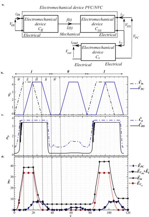
Figure 6. Energy Analysis of a buffer. a) Block-schematic representation of a gate (PVC or NVC). b) Evolution a the buffer’s input voltages. c) Evolution of capacitances 𝐶 and 𝐶 . d) Energy contributions of electrical parts.
b) Energy analysis
In this section, we investigate the energy balance of the design and we show that only a small part of the energy provided by the electrical sources cannot be recovered.
Cg and 𝐶 are two electromechanically coupled transducers having two electrical inputs
and one mechanical output (Figure 6a). The instantaneous electrical energy is given by:
V 𝑖 𝑉 𝑉 𝑖 𝑑𝑡
The instantaneous mechanical energy output of the system is given by:
Eq 17 𝐸 𝑡 𝑓 𝑡 𝑥 𝑡 𝑑𝑡
where 𝑓 𝑡 is the mechanical force applied on the mobile part and 𝑥 𝑡 is its velocity. The expression of 𝑖 and 𝑖 are given by:
Eq 18 𝑖 𝐶 𝑉 𝐶 𝑉 𝑥 𝑡 ,
Eq 19 𝑖 𝐶 𝑉 𝐶 𝑉 𝑥 𝑡 =𝐶
Combining equations 0, 0 and 0, the expression of Ee(t) becomes:
Eq 20 𝐸 𝑡 𝑉 𝑉 𝑉 𝑉 𝑉 𝑥 𝑡 𝑑𝑡 𝐶 2 𝑉 𝐶 2 𝑉 𝐶 2 𝑉 𝐸 𝐸 𝐸 𝐸 𝐸
The first three terms of 0 represent the electrostatic energy stored in the capacitances Cg, Co
and CDS respectively. The last term Em represents the mechanical energy. In other words, the
electrical energy supplying a capacitive transducer is converted in two parts, the electrostatic energy stored in the variable capacitance and the output mechanical energy [27][28].
We have investigated the energy conversion and losses in the CAL buffer shown in Figure 4a, and loaded by a logical sequence 𝑉 (101) (Figure 6b). The variations of 𝐶 and 𝐶 , the non-dimensional values of CDS and Cg (see Table 1) are shown in Figure 6c. During the Wait
interval, 𝑉 increases and a large part of the electrical input energy 𝐸 is stored in 𝐶 (we call it 𝐸 ). The rest is converted into the mechanical energy 𝐸 : part of it is stored in the mechanical springs that moves the body, leading to an increase of 𝐶 and 𝐶 until they reach their maximum values. The remaining energy is converted into kinetic energy and part of it is lost during the impact between the drain and the source electrodes (see the oscillations of 𝐶 and 𝐶 in Figure 6c). During the Evaluate interval, VPC increases, generating an electrical
input energy 𝐸 . However 𝐶 and 𝐶 remain maximum and there is no electromechanical energy conversion: all the electrical energy 𝐸 is stored in 𝐶 and Co.
During the Hold interval, 𝑉 decreases but the capacitances 𝐶 and 𝐶 do not change, as explained previously: only 𝐸 is recovered by 𝑉 . During the Recovery interval, both electrical energies stored in 𝐶 and 𝐶 are recovered by 𝑉 , and 𝐶 remains constant for a while.
The electrical energy necessary to supply the buffer is not fully recovered: some energy is dissipated by damping losses and during the impact. Figure 6d shows the evaluation of the
non-dimensional electric energy 𝐸 produced by the source 𝑉 , the energy 𝐸 stored in 𝐶 , the energy 𝐸 produced by the source 𝑉 and the energy 𝐸 𝐸 stored in both capacitances 𝐶 and Co. During one cycle, with the dimension in table 2 corresponding to a
realistic device of 25 µm², the dissipated energy is equal to 0.9 𝑓𝐽. However, most of the input energy 𝐸 𝐸 is recovered: the ratio between the recovered and the input energy is 89%.
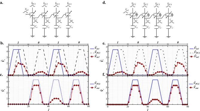
Figure 7. Experiments of cascability. a,d) Tested circuits made of 4 cascaded buffers/inverters. b,c)
Evolution of voltages in cascaded buffers. e,f) Evolution of voltages in cascaded inverters.
c) Cascability
Now we consider the circuit composed of four cascaded CAL buffers and inverters. The buffer and inverter chain circuits are presented in Figure 7a,d respectively. Each gate is supplied by a PC, and the subsequent PCs are delayed by a quarter of period in order to satisfy the adiabatic conditions. The dynamic behavior of the cascaded buffers and inverters is given by the following non-dimensional equation:
(Eq 21) 𝑥 λ𝑥 𝑥 𝑉 , 1 . 𝛼 𝛼 𝑉 ,
𝛼 𝑉 ,
where i refers to the position of the gate in the chain, 𝛼 1 and 𝛼 0, for PVC configuration and 𝛼 𝛼 1 for NVC) and:
(Eq 22) 𝑉 , , ,
(Eq 23) 𝑉 , 𝑉 , 𝐶 , 𝐶 / 𝐶 , 𝐶 , 𝐶 .
We studied the dynamical response of the cascaded elements to an input logic sequence 𝑉 (1010). Figure 7b,e depict the dynamic output of the first gate for the buffer and inverter series. The logic state at the 4th gate for the buffer and inverter series are shown in Figure 7c,f respectively. The high (1) level corresponds to 77 % of the PC’s maximum voltage (equal to 1.38 V) for both buffers and inverters chains, and the low (0) level corresponds to 23 % and 20% of the PC for the buffers and the inverters chains respectively.
4. Conclusion
We have presented novel four-terminal variable capacitors (FTVC) based on silicon nano/micro technologies that can be used in Capacitive Adiabatic Logic. The FTVC intends to replace the field effect transistor (FET) in adiabatic logic in order to drastically reduce the energy consumption by avoiding the static losses and the non-adiabatic dissipation in classical CMOS circuits. It is a better alternative than nanorelays, also envisaged in adiabatic logic using electromechanical devices, because of the absence of resistive contact.
The electromechanical simulations demonstrated that with only two types of FTVC, it is possible to implement basic adiabatic logic functions as inverters and buffers. We also demonstrated for the first time the cascability of both class of devices. During one cycle, a buffer gate of 10x2.5 µm2, dissipated 0.9 𝑓𝐽, which is in the same order of the energy dissipated by nano-scale FET transistors. However, it scales in the cube of the size. Gaining one order of magnitude in volume will allow to beat the dissipation of the state of the art of CMOS circuits: the simulations shows that a buffer gate of 1x0.25 µm² would dissipate 0.7 aJ.
The simulations presented in this paper are performed with dimensions of devices that can be fabricated with classical MEMS and IC technologies. The characteristic dimension is 40 nm for both structures and gaps, and is still possible to achieve using photolithography as in last generations of IC technologies. In addition, there is much less steps in the fabrication process that for ICs and it does not require any expensive material. Reducing even more the dimensions will need the use of e-beam lithography, which is currently still quite expensive because of the longer time required for this step. Etching gaps in silicon at the nanometer scale would be also a challenge. However, reducing the size of the etching areas is very favorable to Deep Reactive Ion Etching of silicon because of an increase of the etching aspect-ratio (AR) with small dimensions: for instance in [29], Parasuraman et al have performed an AR of 125 for a gap of 35 nm.
When adiabatic conditions are satisfied, most of the provided energy (89%) is recovered after one cycle. This is a bit less than the non-contact device we have presented in [19]. However, the logic state differentiation has been dramatically improved from a few percents to more than 50%. This is a considerable advantage for a practical implementation.
5. Aknowledgement
The authors acknowledge financial support from the French Research National Agency (ANR) through the contract #ANR-15-CE24-0013-02.
6. References
[1] S. Houri, G. Billiot, M. Belleville, A. Valentian, H. Fanet, Limits of CMOS Technology and Interest of NEMS Relays for Adiabatic Logic Applications, IEEE TCAS , 62 (2015) 1546–1554. [2] A.P. Chandrakasan , S. Sheng , R.W. Brodersen, Low power CMOS digital design, IEEE
Journal of Solid-State Circuits, 27 (1992) 473–484.
[3] A. Bellaouar, M. Elmarsry, Low Power digital VLSI Design, Circuits and Systems,1995. [4] K. Roy, S. Prasad, Low-power CMOS VLSI Circuit Design, Wiley, 2000.
[5] E. Pop, Energy Dissipation and Transport in Nanoscale Devices, Nano Research, 3 (2010) 147– 169.
[6] P. Teichmann, Adiabatic logic: future trend and system level perspective, Springer Science in Advanced Microelectronics, 2012.
[7] R. Landauer, “Irreversibility and Heat Generation in the Computing Process”, IBM J. Res. Dev, 5 (1961) 183–191
[8] M. Madami, D. Chiuchiù, G. Carlotti, L. Gammaitoni, Fundamental energy limits in the physics of nanomagnetic binary switches, Nano Energy, 15 (2015) 313–320.
[9] H. Fanet, Ultra Low Power Electronics and Adiabatic Solutions, Electronics Engineering Series, ISTE / Wiley edition, 2016 – DOI: 10.1002/9781119006541
[10] Y. Moon, D.K Jeong, An Efficient Charge Recovery logic Circuit, IEEE J. Solid State Circuits, 31(1996) 514-522.
[11] S. Paul , A.M. Schlaffer , J.A. Nossek, Optimal charging of capacitors, IEEE Transactions on Circuits and Systems I: Fundamental Theory and Applications, 47 (2000) 1009–1016.
[12] O.Y. Loh, H.D. Espinosa, Nanoelectromechanical contact switches, Nature Nanotechnology, 7 (2012) 283–295.
[13] Z. Yi, J. Guo, Y. Chen, H. Zhang, S. Zhang, G. Xu, M. Yu and P. Cui, “Vertical, capacitive microelectromechanical switches produced via direct writing of copper wires”, Microsystems & Nanoengineering (2016) 2 16010 - doi: 10.1038/micronano.2016.10
[14] H. Kam, T-J. King Liu, V. Stojanovic, D. Markovic, E. Alon, Design optimization and scaling of MEM relays for ultra-low power digital logic, IEEE Trans. Electron Devices , 58 ( 2011) 236– 250.
[15] C. Pawashe, K. Lin, K.J. Kuhn, Scaling limits of electrostatic nanorelays, IEEE Transactions on Electron Devices, 60 (2013) 2936–2942.
[16] M. Spencer , F. Chen , C. C. Wang , R. Nathanael , H. Fariborzi , A. Gupta , H. Kam , V. Pott , J. Jeon , T-J. King Liu , D. Markovic , E. Alon , V. Stojanovic, Demonstration of Integrated Micro-ElectroMechanical Relay Circuits for VLSI Applications, IEEE Journal of Solid-State Circuits, 4 (2011) 308–320.
[17] S. Houri, C. Poulain, A. Valentian, H. Fanet, Performance Limits of Nanoelectromechanical Switches (NEMS)-Based Adiabatic Logic Circuits, J. Low Power Electron, 3 (2013) 368-384. [18] G. Pillonnet, H. Fanet , S. Houri, Adiabatic capacitive logic: a paradigm for low power logic,
Circuits and Systems (ISCAS), 2017 IEEE International Symposium on, Baltimore, MD, USA, 28-31 May 2017.
[19] A. Galisultanov, Y. Perrin, H. Samaali, H. Fanet, P. Basset and G. Pillonnet, “Contactless four-terminal MEMS Variable Capacitor for Capacitive Adiabatic Logic" , IOP Smart Materials and Structures, vol. 25, no 8, 2018 – DOI:10.1088/1361-665X/aacac4
[20] C.H. Bennett, Logical reversibility of computation, IBM Journal of Research and Development, 17 (1973) 525–532.
[21] J.G. Koller, W.C. Athas, Adiabatic switching, low energey computting, and the physics of storing and erasing information, Physics and Computation, PhysComp '92., Workshop on, Dallas, TX, USA, USA, 2-4 Oct. 1992.
[22] N.P. Vander Meijs, J.T. Fokkema, VLSI circuit reconstruction from mask topology, Integration the VLSI Journal, 2 (1984) 85-119.
[23] S. D. Senturia, “Microsystem design”, Springer US edition, 2001, DOI 10.1007/b117574
[24] H.B. Palmer, Capacitance of a parallel-plate capacitor by the Schwartz–Christoffel transformation, Transactions of the American Institute of Electrical Engineers, 56 ( 1937 ) 363– 366.
[25] A. Tazzoli, M. Barbato, Study of the actuation speed, bounces occurrences, and contact reliability of ohmic RF-MEMS switches . Microelectronics Reliability 50 , (2010)1604–1608.
[26] A. Peschot , C. Poulain , N. Bonifaci , O. Lesaint, . Contact Bounce Phenomena in a MEMS Switch . IEEE 58th Holm Conference on Electrical Contacts (Holm), (2012).
[27] T. B. Jones, N. G. Nenadic, Electromechanics and MEMS. Cambridge University Pres, 2013. [28] G. M. Rebeiz, RF MEMS: theory, design, and technology, John Wiley & Sons, 2004.
[29] J. Parasuraman, A. Summanwar, F. Marty, P. Basset, D. E. Angelescu, C. Bunel and T. Bourouina, “Very High Aspect Ratio Deep Reactive Ion Etching of Sub-micrometer Trenches in Silicon”, Microelectronics Engineering, vol. 113, pp. 35-39, Jan. 2014
Dr. Hatem Samaali obtained his Ph.D. degree in Microelectronics from National Engineering School of Sfax (ENIS), Tunisia in 2011. He was a post-doc at ESIEE Paris, France, from 2016 to 2018 where he worked on NEMS-based adiabatic circuits. His current research topics include nonlinear dynamics in NEMS/MEMS Switch devices and Energy Harvesting.
Dr. Yann Perrin was born in Fontainebleau, France, in 1989. He received his Master's degree in Nanophysics from the University of Paris-Sud, and his Ph.D in nanomagnetism from the University of Grenoble, in 2013 and 2016, respectively. He joined the CEA-LETI, France, in 2016 as a post-doctoral fellow. His research interests include energy-efficient circuits, and circuit design with novel devices such as micro electromechanical systems (MEMS).
Dr. Ayrat Galisultanov received the Ph.D. degrees in Engineering from Avangard JSC, St. Petersburg, Russia in 2013 with research focus on SAW force sensor. From September 2009 to March 2015, he was an R&D engineer at Avangard JSC. Ayrat Galisultanov was a postdoctoral researcher with FEMTO-ST Institute, Besançon, France prior to his current position of a postdoctoral researcher in CEA-LETI, Grenoble, France. His research interests include novel capacitive-based adiabatic logic devices, microelectromechanical systems, and SAW sensors.
Hervé Fanet received in 1971 the engineer’s diploma from the “Ecole Supérieure d’Electrricité”. He was involved in detectors and electronic developments for high energy particle Physics. He joined
CEA-LETI in 1996 and was in charge of medical imaging research and manager of integrated circuits design department. His current research topics include smart sensors and ultra-low power electronics. He has published 40 papers in journals and is author or co-author of five books
Dr.Gaël Pillonnet was born in Lyon, France, in 1981. He received his Master’s degree in Electrical Engineering from CPE Lyon, France, in 2004, a PhD and habilitation degrees from INSA Lyon, France in 2007 and 2016, respectively. Following an early experience as analog designer in STMicroelectronics in 2008, he joined the University of Lyon in the Electrical Engineering department. During the 2011-12 academic year, he held a visiting researcher position at the University of California at Berkeley. Since 2013, he has been a full-time researcher at the CEA-LETI, a major French research institution. His research focuses on energy transfers in electronic devices such as power converter and amplifier, energy-recovery logic, mechatronics systems, scavenging interfaces.
Dr. Philippe Basset is professor at Université Paris-Est / ESIEE Paris. He received his Ph.D from IEMN / University of Lille in 2003 in the areas of microelectronic and micro-electro-mechanical-systems (MEMS). In 2004 he was a post-doc at CMU, Pittsburgh, USA and he joined ESIEE Paris in 2005. His current research interests include micro-power sources for autonomous MEMS and micro/nano-structuration of silicon. He serves in the International Steering Committee of the PowerMEMS conference since 2015 and is currently deputy director of the ESYCOM laboratory.