An Automated Bench Testing System
for Direct Current Parameters of Instrumentation Amplifiers
by
Arthur Musah
Submitted to the Department of Electrical Engineering and Computer Science
in Partial Fulfillment of the Requirements for the Degrees of
Bachelor of Science in Electrical [Computer] Science and Engineering
and Master of Engineering in Electrical Engineering and Computer Science
at the Massachusetts Institute of Technology
MASSACHUSETTS INSTITUTE
May 18, 2005 OF TECHNOLOGY
Copyright 2005 Arthur Musah. All rights reserved.
JUL 182005
LIBRARIES
The author hereby grants to M.I.T. permission to reproduce anddistribute publicly paper and electronic copies of this thesis and to grant others the right to do so.
-Author
Department of Electrical Engineering and Computer Science
May 17, 2005
Certified
by__ _//__-__ _ _
Mark Irwin
VI-7 " eenrvisorq11i
Certified by___ _ _ _ _ _ _ _ _ _ _7 en K. Burns Supervisor AcceF by_______ .hur C. Smith iduate Theses
An Automated Bench Testing System
for Direct Current Parameters of Instrumentation Amplifiers
by Arthur Musah
Submitted to the
Department of Electrical Engineering and Computer Science
May 18, 2005
In Partial Fulfillment of the Requirements for the Degree of Bachelor of Science in Computer [Electrical] Science and Engineering and Master of Engineering in Electrical Engineering and Computer Science
ABSTRACT
Electrical testing is performed at multiple stages in the production of analog integrated circuits (ICs). An efficient system for low-volume IC testing is one that automates bench tests and provides good measurement precision and accuracy, while costing far less than the standard automated test equipment (ATE) used for high-volume manufacturing purposes. This thesis describes the design and implementation of an automated bench system for measuring the important direct current parameters associated with analog instrumentation amplifiers: voltage offset, input bias currents, input offset current, output swing, common mode rejection, power supply rejection, quiescent current and gain error. The system is developed on the PXI platform and consists of measurement and signal generating hardware modules, a Windows-based computer, a resource printed circuit board (PCB), a test-configuration PCB and LabVIEW-based software. The system is versatile and supports the testing of different instrumentation amplifier types and pin-outs. The performance of the system is characterized with respect to ATE results for the Texas Instruments instrumentation amplifier INA126.
Thesis Supervisor: Stephen K. Bums
Acknowledgements
I am grateful to my supervisors Mark Irwin and Stephen Bums for their ideas, guidance
and support in this project. I am thankful to Sergio Hidalgo for the many discussions we had about aspects of the system and for designing the Resource Interface Board for the system. My gratitude also goes to Jerry Riddick for his discussion of instrumentation amplifier testing, to Susan Madaras for performing miraculous soldering jobs on my printed circuit board, to Joline Albaugh for all her help with obtaining components, and to the entire High Performance Analog Product Optimization team at Texas Instruments for an incredible learning experience.
Contents
C H A PTER 1 IN TR O D U C TIO N ... 10
1.1 MOTIVATION FOR AN AUTOMATED BENCH TESTING SYSTEM ... 10
1.2 PREVIOUS W ORK ... 11
1.3 INSTRUM ENTATION A M PLIFIERS ... 12
1.3.1 The Ideal Instrum entation A mplifier ... 14
1.3.2 The R eal Instrum entation A mplifier ... 15
1.3.3 IN A 126P Param eter Specifications ... 17
1.4 O VERVIEW OF THE A UTOM ATED BENCH SYSTEM ... 18
CHAPTER 2 TEST METHODS FOR DC PARAMETERS... 20
2.1 M EASURING V O S ... 20
2.2 M EASURING PSR R ... 22
2.3 M EASURING C M R R ... 22
2.4 M EASURING IQ ... 24
2.5 M EASURING IB+, IB- AND IO S ... 25
2.6 M EASURING SW + AND SW -... 26
2.7 M EASURING G ER R ... 27
C H A PTER 3 SY STEM H A R D W A R E ... 28
3.1 R ESOURCE H ARDW ARE ... 29
3.1.1 PX I Chassis... 29
3.1.2 D igital I/O M odule... 29
3.1.3 A nalog O utput M odule... 30
3.1.4 Signal M uxes ... 30
3.1.5 D igital M ultim eter M odule... 31
3.1.6 Power Supplies... 31
3.1.7 R esource Interface B oard... 31
3.2 TEST C ONFIGURATION BOARD ... 33
3.2.1 R esource Interface Connectors... 36
3.2.2 Voltage R egulators... 36
3.2.3 Input Circuitry ... 37
3.2.4 D U T Interface... 41
3.2.5 O utput M easurem ent Circuitry ... 43
3.3 D U T SOCKET A DAPTERS ... 45
3.4 THE D ESKTOP C OM PUTER ... 45
C H A PTER 4 SY STEM SO FTW A R E ... 47
4.1 THE A UXILIARY SUBV IS ... 49
4.1.1 IA Power to Board R egulators ON ... 49
4.1.2 IA Power to Board R egulators OFF ... 50
4.1.3 IA Set D U T Supplies... . 51
4.1.4 IA D U T Supplies O FF ... 52
4.1.5 IA SE T Selected R elays ... 53
4.1.6 IA RESE T Selected R elays ... 55
4.1.7 IA RESE T A LL R elays... 56
4.1.8 IA O utput CM Voltage Gain3 ... 57
4.1.9 IA O utput M D A C Voltage ... 58
4.1.10 IA Select M UX N O utput... 59
4.1.11 IA Select M UXP O utput ... 61
4.1.12 IA E nable M UX N ... 61
4.1.13 IA E nable M UX P ... 62
4.1.15 IA D isable M UXP ... 62
4.1.16 IA Select Voltage Amplifier ... 63
4.1.17 IA Select PGA Gain ... 63
4.1.18 M easure EAJVO UT ... 64
4.1.19 M easure EA2_VO UT ... 66
4.2 THE PARAMETER TEST SUBVIS... 66
4.2.1 The Test VOS Sub VI ... 66
4.2.2 The Test PSRR Sub VI ... 67
4.2.3 The Test CM RR Sub VI... 68
4.2.4 The Test IQ SubVI... ... 69
4.2.5 The Test IB Sub VI ... 70
4.2.6 The Test SWIN G Sub VI ... 72
4.2.7 The Test GERR SubVI ... 74
4.3 THE SINGLE CHANNEL INSTRUMENTATION AMPLIFIER TEST PROGRAM ... 75
CHAPTER 5 SYSTEM PERFORMANCE ANALYSIS... 78
5.1 THE ANALYSIS CRITERIA ... 78
5.2 ANALYSIS OF V O S MEASUREM ENTS... 81
5.3 ANALYSIS OF PSRR M EASUREMENTS... 82
5.4 ANALYSIS OF CM RR M EASUREMENTS... 84
5.5 ANALYSIS OF IQ + M EASUREM ENTS ... 85
5.6 ANALYSIS OF IB+, IB- AND IO S M EASUREMENTS... 86
5.7 ANALYSIS OF SW + AND SW - M EASUREM ENTS... 88
5.8 ANALYSIS OF G ERR M EASUREMENTS... 88
5.9 TEST DURATION ... 89
CHAPTER 6 FUTURE WORK AND CONCLUSIONS ... 90
6.1 M EASURING RESISTORS... 90
6.2 RESULT AVERAGING ... 91
6.3 O PTIM IZATION OF DELAYS... 91
List of Figures
Figure 1. The functional model of an instrumentation amplifier... 12
Figure 2. The internal topology of a "difference amp" type instrumentation amplifier. 13 Figure 3. The internal topology of the "3 op-amp" type instrumentation amplifier... 14
Figure 4. The internal topology of the "2 op-amp" type instrumentation amplifier... 14
Figure 5. Connections between components of the AutoBench system indicate signal or inform ation flow s... 19
Figure 6. The first step of the test configuration used to measure VOS... 21
Figure 7. The second step of the VOS measurement is a reading of the error contributed by the output am plification circuitry... 21
Figure 8. The test configuration for measuring IQ of an instrumentation amplifier. ... 25
Figure 9. The configuration for measuring the bias and offset currents of an amplifier's in p u ts... 2 6 Figure 10. The assembled instrumentation amplifier AutoBench system... 28
Figure 11. A PCB drawing of the Resource Interface board showing the connectors and signal traces... 32
Figure 12. The PCB diagram for the INA Test Configuration Board, showing the signal layers and device footprints. ... 34
Figure 13. Voltage regulators on the INA Test Configuration Board adapt the 25V external supplies to the voltages required by the active devices on the board. ... 36
Figure 14. Voltages are generated with an Analog Output channel and amplified by a high voltage op-amp to produce the Single Ended Voltage (SEV) resource... 38
Figure 15. A 16-bit DAC is used to generate the Precision Differential Voltage, PDV, reso u rce ... 3 9 Figure 16. Direct ground paths and resistive paths to the ground signal are available for the inputs of the D U T. ... 40
Figure 17. The DUT power is supplied through a resistor to enable measurement of the current flowing into the DUT supply pins. ... 41
Figure 18. The DUT interface connections to multiple inputs, multiple gain-setting resistors, and multiple loads. Support for dual channel amplifier packages is included. Relays are used to swap between the possible configurations... 42
Figure 19. The output measurement circuitry includes multiple amplification paths to support signals of different characteristics. The output signals are measured differentially. Analog multiplexers are used to select the signals for the amplification stag e . ... 4 4 Figure 20. A PCB diagram for the DUT socket adapters. ... 45
Figure 21. The front panel for a LabVIEW virtual instrument... 47
Figure 22. The block diagram for a LabVIEW virtual instrument. ... 48
Figure 23. Program flow for the IA Power to Board Regulators ON subVI. ... 50
Figure 24. Program flow for the IA Power to Board Regulators OFF subVI... 51
Figure 25. Program flow for the IA Set DUT Supplies subVI. ... 52
Figure 26. Program flow for the IA DUT Supplies OFF subVI... 53
Figure 27. Program flow for the IA SET Selected Relays subVI... 55
Figure 28. Program flow for the IA RESET Selected Relays subVI... 56
Figure 30. Figure 31. Figure 32. Figure 33. Figure 34. Figure 35. Figure 36. Figure 37. Figure 38. Figure 39. Figure 40. Figure 41. Figure 42. Figure 43. Figure 44. Figure 45. Figure 46. sigma Program flow Program flow Program flow Program flow Program flow Program flow Program flow Program flow Program flow Program flow Program flow Program flow Program flow Program flow
The graphical user interface for the Single Channel INA Test Program. ... 76
Program flow for the Single Channel INA Test Program subVI. ... 77
A normal (Gaussian) distribution has 99.73% of its probability within a 6 range centered on the m ean ... 79
for the IA Output CM Voltage Gain3 subVI... 58
for the IA Output MDAC Voltage subVI... 59
for the IA Select MUXN Output subVI. ... 60
for the IA Enable MUXN subVI. ... 62
for the IA Select Voltage Amplifier subVI. ... 63
for the IA Select PGA Gain subVI... 64
for the Measure EAl VOUT subVI. ... 65
for the Test VOS subVI... 67
for the Test PSRR subVI... 68
for the Test CMRR subVI. ... 69
for the Test IQ subV I... 70
for the Test IB subV I... 71
for the Test SWING subVI... 73
List of Tables
Table 1. Specifications for the direct current parameters of the INA126P amplifier... 17
Table 2. Bill of materials for the INA Test Configuration Board... 35
Table 3. The mapping of the Digital I/O lines to relay controls... 54
Table 4. The mapping of amplification stage input signals to the analog multiplexer sw itch es... 6 0 Table 5. The mapping of DIO lines to control signals for MUXN... 61
Table 6. The mapping of DIO lines to control signals for MUXP. ... 61
Table 7. The mapping of the amp selection relay states to output amplifier selected.... 63
Table 8. The mapping of control signals to PGAmp gain. ... 64
Table 9. Statistical data for the VOS test... 81
Table 10. The precision of the VOS test... 82
Table 11. The accuracy of the VOS test. ... 82
Table 12. Statistical data for the PSRR test. ... 83
Table 13. The precision of the PSRR test... 83
Table 14. The accuracy of the PSRR test. ... 83
Table 15. Statistical data for the CMRR test. ... 84
Table 16. The precision of the CMRR test. ... 84
Table 17. The accuracy of the CMRR test... 85
Table 18. Statistical data for the IQ+ test. ... 85
Table 19. The precision of the IQ+ test. ... 86
Table 20. The accuracy of the IQ+ test... 86
Table 21. Statistical data for the IB+, IB- and IOS tests... 86
Table 22. The precision of the input offset current test... 87
Table 23. The accuracy of the input offset current test... 87
Table 24. Statistical data for the GERR test. ... 88
Table 25. The precision of the GERR test... 89
Chapter 1
Introduction
1.1 Motivation for an Automated Bench Testing System
Electrical testing is a routine and essential task performed at multiple stages in the production of integrated circuits (ICs). Manufacturing involves the probing of individual dies for critical electrical parameters at the wafer stage. This probing permits the manufacturer to monitor yields and to avoid wasting assembly time on bad die. In later stages of manufacturing, when the ICs have been assembled into packages, a final test of select electrical parameters is usually performed again in order to ensure that only devices that meet product data sheet specifications are shipped out. Outside manufacturing, engineers need to be able to electrically test ICs for the purposes of investigating device failures or for the qualification of new integrated circuit products. It is in this other kind of testing, which usually involves a few rounds of testing some tens or hundreds of units, that a need arises for a custom testing solution.
Automatic test equipment (ATE) used by semiconductor manufacturers to test packaged ICs before delivering them to customers costs hundreds of thousands of dollars to acquire and is expensive to operate. Therefore, the available automatic test resources within a company are typically limited and are utilized for a broad range of testing tasks, from manufacturing to product development and product support. Manufacturing purposes generally make fuller use of the features and high-speed functionality of ATE, and have the highest priority for test time on the ATE. Product development, characterization, qualification and support take lower priority. Often, the lower priority non-manufacturing tasks need only to be able to test low volumes of ICs and therefore do not need the high throughput demanded by manufacturing. The expensive high-speed capability of the test equipment is therefore superfluous in non-manufacturing testing.
Bench tests are often employed by engineers when only a few devices need to be tested as part of non-manufacturing tasks. Bench testing is generally a makeshift, highly
devices, etc. Bench testing involves manually setting up the test conditions for the device to be tested, applying the inputs, measuring some outputs, perhaps doing a few quick calculations and recording the data obtained. It is a quick avenue available for an electrical engineering probing a problem and is an extremely versatile and therefore useful method of performing electrical tests.
However, as the number of devices increases from two to a few tens to some hundreds, the need for automation of the testing arises. At this point an automated test system that provides acceptable trade-offs in speed and versatility for a gain in affordability and suitability becomes very attractive. Marrying the most suitable ideas from the two extremes of ATE and bench testing, one comes up with the concept of the automated bench testing system.
This thesis is concerned with the design, building and characterization of an automated bench testing system for measuring the properties of instrumentation amplifiers from Texas Instruments Incorporated. The overarching objective for the successful implementation of the system was to have the capability of measuring the DC parameters of a broad range of instrumentation amplifier types at speeds lower than those
obtained from ATE but with comparable accuracy.
1.2 Previous Work
A precise and accurate automated bench system for measuring the direct current parameters of operational amplifiers has previously been implemented. [1] Although the
operational amplifier (op-amp) system measures parameters similar to those of instrumentation amplifiers, the circuitry and resources necessary for performing the instrumentation amplifier tests are different and demand the implementation of a unique solution. The PXI hardware platform and the LabVIEW software development environment used in the op-amp solution are also employed in the new test system implemented herein for instrumentation amplifiers.
1.3 Instrumentation Amplifiers
Instrumentation amplifiers are electrical devices that perform amplification of differential input signals to a high degree of accuracy. Instrumentation amplifiers are also characterized by their ability to reject common mode input signals very effectively. As a consequence of these two key properties instrumentation amplifiers can be used to measure very small differential voltages to a high degree of accuracy and are especially suitable for instrumentation applications, hence their name.
An instrumentation amplifier device generally has an inverting and a non-inverting input pin, two power supply pins, two pins across which a gain-setting resistor can be connected, an output pin and an output reference pin. This functional model of an instrumentation amplifier is represented in Figure 1.
Invert Non-ir input Gain-setting pin 1 Gain-setting
Positive supply pin 2
voltage U5 ing input Output ou IN+ verting INAmp
Negative Output reference
Different internal architectures or topologies exist for integrated circuit instrumentation amplifiers, but all consist of networks of op-amp building blocks and high-precision resistors. Instrumentation amplifiers are distinctly different from op-amps because feedback is often implemented internally in the former. The most common types are the difference amplifier, the two amp instrumentation amplifier and the three op-amp instrumentation op-amplifier [2].
The difference amplifier type instrumentation amplifier is shown in Figure 2. This consists of one op-amp with high-precision resistors. The feedback and input resistor combination R2 and RI determine the amplifier gain. Occasionally, the end of R2 connected to the output is left unwired and brought out as a separate pin for the user to connect directly to the output for the default gain or via an extra resistor to change the gain. An example of a TI instrumentation amplifier with this topology is the INA132.
R2 Output Inverting input R1 R3 Non-inverting R4 input Output reference
Figure 2. The internal topology of a "difference amp" type instrumentation amplifier.
The three op-amp instrumentation amplifier has three op-amps and precision resistors connected as shown in Figure 3. An example of at TI device with this topology is the
Inverting input Gain resistor pin 1 RG Gain resistor pin 2 Non-inverting input Output R1 R2 --- RF1 RF2> R3 R4
Figure 3. The internal topology of the "3 op-amp" type instrumentation amplifier.
Figure 4 shows the two-op-amp instrumentation amplifier topology, which is used in the TI device INA126. Gain resitor RG pin 1 1 Reference Inverting input Non-inverting input R1 Gain resistor pin 2 RF1 R2 RF2
Figure 4. The internal topology of the "2 op-amp" type instrumentation amplifier.
Output Output
inputs. This characteristic is constant over its entire specified power supply voltage and common mode input voltage ranges. It draws no current from its supplies when it is not loaded, and no current flows into or out of its inputs. Its gain is perfectly linear and accurately defined by a characteristic gain equation. Its output voltage is capable of rising as high as the positive power supply voltage and dropping as low as the negative supply voltage.
In reality, however, the above properties do not hold. Quantification of the limitations of the above mentioned properties in a real amplifier give rise to the parameters defined in the next section.
1.3.2 The Real Instrumentation Amplifier
The parameters measured by the AutoBench system are frequently referred to as the direct current (DC) parameters of an instrumentation amplifier. They are so called because their measurement involves direct current inputs and outputs. Typically, most of the parameters specified in the manufacturer's data sheet for an instrumentation amplifier are DC parameters. [3]
The bench system's functionality was restricted to the DC parameters because these are the most frequently measured parameters in development, qualification and support related testing of instrumentation amplifiers. Supporting less frequently used AC parameters such as amplifier bandwidth and slew rate would have increased the complexity of the bench testing system without commensurately improving the system's utility.
The AutoBench system was designed to be capable of measuring the following
DC parameters: input offset voltage, input bias and offset currents, power supply
rejection, quiescent current, common mode rejection, output swing and gain error.
1.3.2.1 Input Offset Voltage (VOS)
Input offset voltage (VOS) is the voltage that shows up at the output of the amplifier when the amplifier's inputs are grounded, i.e. both inputs are zero and common mode is zero. In a real instrumentation amplifier the VOS is non-ideal and is therefore not
zero as would be expected in the perfect situation. The VOS parameter gives a measure of the goodness of the amplifier, with smaller VOS being better.
1.3.2.2 Power Supply Rejection Ratio (PSRR)
The power supply rejection (PSR) is an indication of how the VOS of an instrumentation amplifier changes with respect to variations in the power supply voltages. PSRR is defined as the ratio of the change in VOS to the causative change in power supply voltages. The parameter is determined by measuring VOS, with inputs grounded, at each of the extremes of the power supply range and calculating the desired ratio. PSRR is reported in units of V/V or as PSR in units of dB.
1.3.2.3 Common Mode Rejection Ratio (CMRR)
Common mode rejection (CMR) is an indication of how the VOS of an instrumentation amplifier changes with respect to variations in the common mode voltage at the inputs of the amplifier. CMRR is defined as the ratio of the change in VOS to the causative change in common mode voltage. The parameter is determined by simultaneously connecting both inputs of the amplifier to different voltages within the acceptable range of common mode inputs defined for the device, and measuring the output voltage. Essentially this is a measure of VOS, with both inputs connected to non-zero voltages. The power supplies and all other factors are kept constant for all measurements. CMRR is reported in units of V/V or as CMR in dB.
1.3.2.4 Quiescent Current (IQ)
Quiescent current is the current drawn by the instrumentation amplifier when its output is not loaded and the inputs are both grounded. This parameter is an indication of the power consumption of the amplifier when it is not being used but its supplies are connected. It is a useful parameter to know in the design of an application that uses an instrumentation amplifier as it allows one to determine if power to the device needs to be cut off or can be left on. IQ is also a useful parameter to test if one wants to make a quick
1.3.2.5 Input Bias Currents (IB+ and IB-) and Input Offset Current (IOS)
The input bias current (IB) of an instrumentation amplifier is the current flowing into or out of its input. IB+ is used to denote the bias current associated with the non-inverting input of the amplifier while IB- is used to denote the bias current associated with the inverting input. The sum of IB+ and IB- is the input offset current (IOS).
1.3.2.6 Output Swing (SW+ and SW-)
The output swing of an instrumentation amplifier is the specification of how close the voltage at the amplifier output can get to the amplifier's rail, i.e. the power supply voltage. Two values are specified: one for the swing to the positive rail, the positive swing (SW+), and the other for the swing to the negative rail, the negative swing (SW-).
1.3.2.7 Gain Error (GERR)
The gain error parameter is a measure of how the actual gain of the instrumentation amplifier deviates from the ideal gain. The gain error is reported as a percentage of the expected gain derived from the amplifier's gain equation for the particular configuration of gain-setting resistors.
1.3.3 INA126P Parameter Specifications
The range of values for the supported instrumentation amplifier test parameters are shown in Table 1. [3]
Parameter Symbol Minimum Typical Maximum Unit
Input offset voltage VOS +/-100 +/-250 uV
Power supply rejection PSRR 5 15 uV/V
Common mode rejection CMRR 83 94 dB
Quiescent current IQ +/-175 +/-200 uA
Input bias current IB -10 -25 nA
Input offset current lOS +/-0.5 +/-2 nA
Positive output swing SW+ (V+)-0.9 (V+)-0.75 V
Negative output swing SW- (V-)+0.95 (V-)+0.8 V
Gain error GERR +/-0.02 +/-0.1 %
The gain of the INA 126 instrumentation amplifier is defined by Equation 1.
Gain = 5 + 80,000/RG (Eq. 1)
RG in Equation 1 is the value of the setting resistor connected across the two
gain-setting pins of the instrumentation amplifier. Therefore, the gain of the INA 126 amplifier is 5 when there is no connection between the gain-setting pins since the resistance across them is infinite.
1.4 Overview of the Automated Bench System
The automated bench (AutoBench) system consists of hardware and software. The hardware is developed on the PXI platform, which allows for integration of multiple instrumentation devices into a system controlled by a desktop computer. Two printed circuit boards (PCBs) are designed for the system. A Resource PCB is used to provide a compact and organized interface to the bulky resources and the many cables of the PXI devices. A Test Configuration PCB mounts on top of the Resource PCB and implements the circuits needed for testing instrumentation amplifiers. The hardware is designed for versatility and the Resource Board interface allows for test solutions for other device families to be developed on the system.
Software is developed in the LabVIEW graphical programming environment, which is especially conducive for PXI platform development due to the availability of device support. An overview of the system is shown in Figure 5.
DUT TestConfigPCB Resource PCB Power 1 Power 2
GPIB DIO AO Mux1 Mux2 DMM
D esktop PC with MXI-3 PCI Card instal e d
Figure 5. Connections between components of the AutoBench system indicate signal or information
Chapter 2
Test Methods for DC Parameters
The procedure for measuring a parameter generally involves the configuration of appropriate gain and load, the selection of inputs to the DUT, the selection of the DUT channel being tested, the conditioning and reading of outputs, and the calculation of the parameter value. The methods used to measure each of the parameters above are described in the following subsections.
2.1 Measuring VOS
The VOS is measured on the AutoBench system by grounding both inputs of the
DUT, powering the DUT, and taking a reading of the voltage at the output. The DUT
gain and load resistances are configured as necessary for the device being tested. The output reference pin of the DUT is at ground. Due to the small (usually microvolt) value of the VOS, the output voltage at the DUT is gained up with the programmable gain amplifier- (PGA-) based amplification circuitry before being read with the digital multimeter. The setup for the measurement is shown in Figure 6. The voltage reading obtained in this first step of the VOS measurement is named VoutA and its value is given
by Equation 2.
Errors are introduced in the VOS value of the DUT by the offset voltages of the devices in the gaining up stage. Therefore an extra reading is obtained with the PGA-based amplifier inputs connected to ground as shown in Figure 7. This second reading, named VoutB, has a value defined by Equation 3. The two readings are used to derive an accurate value for the DUT VOS in software by using Equation 4.
DUT Ampi Ampi (VOS, Gdut) (vl,gl) (v2,g2) U In-VOS*Gdut UT YoutA GenericAmp GND DUTRef GND
Figure 6. The first step of the test configuration used to measure VOS.
Ampi Ampi
(vl,gl) (v2,g2)
+ VoutB
DUTRef GND
Figure 7. The second step of the VOS measurement is a reading of the error contributed by the output amplification circuitry.
VoutA = -VOS - lGDUT g g2 + A -gl g g2 + v2 g2
(Eq. 2)
VoutB =vl- gl g2+v2 - g2 = Verr
VOS = VoutA -VoutB -- GDUT .gl.g2
(Eq. 4)
2.2 Measuring PSRR
Power supply rejection ratio (PSRR) is an indication of how the VOS of an instrumentation amplifier changes with respect to changes in the power supply voltages. Therefore, it is determined by varying the power supply voltages across the extremes of the specified supply range and determining the resulting variation in the VOS.
The DUT gain and load resistances are configured as necessary for the device being tested. The inputs are grounded as in the VOS test. The smallest supply range, VSrangel, is applied to the DUT supply pins and the voltage at the output of the amplifier is measured as VI. Then the largest supply range is applied to the DUT supply pins and the voltage at the output of the amplifier is measured as V2. PSRR is then calculated as the ratio of the difference in the output voltages measured to the difference in the supply voltage ranges applied, as in Equation 5.
There is no need for a separate error voltage reading in the PSRR determination. The error voltages introduced by the amplification circuitry stay the same for the two output voltage readings and get eliminated in the subtraction.
PSR R =2V xI
VSrange2 - VSrangel GDUT -GPGA
(Eq. 5)
parameter, the CMR of the amplifier is assumed to be approximately linear and a reading of the VOS is taken at two common mode voltages at the DUT inputs.
The common mode rejection test can be done either with the DUT inputs connected together and therefore at the exact same common mode voltage, or with the
DUT inputs connected across a source imbalance resistance or capacitor and resistor pair.
The latter option allows for the CMRR test to be done in a manner that simulates a real-world situation where the impedances of the sources connected to the DUT inputs are often not equal. The data sheets for instrumentation amplifiers usually specify a source imbalance value; therefore inclusion of support for a CMRR test with source imbalance was seen to be useful.
In the first type of CMRR test, the common mode voltage is applied to the two
DUT inputs directly since they are connected together. In the second type of CMRR test,
the common mode voltage is applied to one DUT input directly and to the other DUT input across the source imbalance. The results are generally similar.
To perform the test, the DUT is placed in the desired gain-setting and load configurations. The DUT is powered. A common mode voltage (VINlo) in the negative common mode voltage range is applied to the inputs and the corresponding output voltage, VOUTlo, is measured. A second common mode voltage (VINhi), this time in the positive common mode voltage range, is applied to the DUT inputs and the corresponding output voltage, VOUThi, is measured. The output voltage measurements are taken by the digital multimeter after amplification of the voltages by the PGA-based amplifier. The CMRR is determined by calculating the ratio of the difference in output voltages to the difference in common mode input voltages and compensating for the gains of the DUT and the amplification circuitry. This ratio is shown in Equation 6. As with the PSRR test, there is no need to perform a separate error measurement for the
amplification circuitry as these errors get eliminated in the subtractions.
CMR VOUThi - VOUT10o ( 1
VINhi -VINlo GDUT -GPGA
2.4 Measuring IQ
IQ is the current an amplifier draws when its output is not loaded. For this test the DUT supply voltage (VS) is supplied from the power supply unit through a high-current
high-voltage operational amplifier buffer with a small known resistance, R, at its output. The voltage after the resistor, labeled DUT VS in the Figure 8, is what is applied to the supply pin on the DUT.
The current is determined by measuring the voltage across the known resistance R, and applying a simple Ohm's law calculation. In addition, an empty socket current value is subtracted from the current value obtained to compensate for the leakage current of this setup. The empty socket current value is determined prior to the parameter test by performing an IQ test with the DUT socket empty.
The potential difference across the known resistance R is determined by applying the voltage at the two ends of the resistor to the inputs of a difference amplifier. The difference amplifier (INA145) has a much higher common mode voltage range (+/-28V) than the other amplification devices and accurately measures the differential voltage at its inputs, i.e. the potential drop across R. The PXI signal multiplexer module is then used to channel the output voltage of the difference-amplifier to the digital multimeter which reads the voltage. The software adjusts for the gain of the difference amplifier (statically configured to 101) and calculates the current according to Equation 7.
This IQ derivation procedure is performed in turn for the negative and positive
DUT supplies in order to obtain readings for IQ- and IQ+ respectively. The other DUT
supply pin is driven through the buffer normally while the complementary supply pin's
IQ value is being determined.
IQ = VI RVV2 X G
j
'QempysocketAMP
--- ~R DUT VS > U2 In-V1 V2 UT 0 GenericAmp GND DUTRef
Figure 8. The test configuration for measuring IQ of an instrumentation amplifier.
2.5 Measuring IB+, IB- and IOS
The bias current for each DUT input is derived from two measurements. First, a measurement equivalent to that performed in the first VOS step is taken. The inputs to the
DUT are both grounded, the DUT output voltage is gained up by the PGA-based
amplifier and the voltage is read with the digital multimeter as VOUTgnd. Second, the
DUT input for which the bias current is being determined is connected to ground via a
1OMQ resistor, while the other input is connected directly to ground. The DUT output voltage is again gained up and read as VOUTbias. The contribution to the DUT input offset due to the bias current on the one input is then calculated as the difference in the two output voltages measured divided by the 10MCI resistance through which the bias current was flowing. The IB corresponding to the input under consideration is then obtained by compensating for the DUT and amplification stage gains. Again, the errors from the amplification stage are eliminated in the subtraction and do not need to explicitly accounted for in the procedure. The derivation is given by the formula in Equation 8. The setup for the IB measurements is shown in Figure 8.
IB = VOUTgnd
C
- VOUThias(
1 IMG ) GDUT GAM,Relay
R1
GND
DUT Ampi Ampi
(Gdut) (gl) (g2) U2 In-UT Vu In+ + YO Relay DUT R2 4 K j DUTRef GND GND
Figure 9. The configuration for measuring the bias and offset currents of an amplifier's inputs.
2.6 Measuring SW+ and
SW-The output voltage swing test involves applying a differential signal to the DUT
by applying a voltage from the SEV generator to the non-inverting DUT input and
grounding the inverting DUT input. The value of the differential input voltage used is the value of the power supply voltage to which the output is to be railed, attenuated by the
gain of the DUT.
The output of the DUT is then compared with the appropriate supply voltage using the difference amplifier output path, which has a high common mode voltage range. The difference amplifier performs a subtraction of the supply voltage and the DUT output voltage, multiplies the result by its gain of 101 and the result is measured using the digital multimeter.
The high gain of 101 proves problematic in the testing stage of the system. Therefore the PGAmp in gain configuration 1 was used to perform a swing test at lower
2.7 Measuring GERR
The gain error parameter test involves the application of a zero common mode differential signal of high precision to the DUT inputs and determining how close the output voltage of the amplifier is to the voltage promised by the gain equation.
A 1OV reference voltage used by the Precision Differential Voltage generator is
used as the gold standard voltage to which the DUT output voltage is compared. Thus the
DUT output voltage is always expected to be 1OV in the GERR tests. The DUT is put into the desired gain configuration. The PDV generator is then used to provide input voltages whose difference equals the gold standard divided by twice the DUT gain. The
1OV reference and the DUT output are then fed to the output amplification circuitry, where a PGA-based amplifier is used to perform a subtraction of the two signal values. To improve the accuracy of the measurement, the inputs to the amplification stage are flipped and another reading is taken. The two readings are added and divided by 2 to remove offset voltage contributions from the output amplifiers and the GERR is calculated as shown by Equation 9.
GERR= V2
-2
GP(GA
00)(Eq. 9)
The hardware is set up as shown in Figure 6 for the first part of the VOS test, except the inputs are not grounded.
System Hardware
Figure 10. The assembled instrumentation amplifier AutoBench system.
The AutoBench system hardware consists of the following components:
1. Resource Hardware 2. Test Configuration Board
3. DUT Socket Adapters
4. Desktop Computer with MXI-3 Link
A picture of the assembled test system is shown in Figure 10.
3.1 Resource Hardware
The National Instruments PXI (PCI Extensions for Instrumentation) platform provides a wide range of hardware modules that can be interfaced to a personal computer for control and automation of custom test solutions. [4] The AutoBench system was designed on this platform and consists of the following PXI modules: PXI Chassis, Digital I/O, Analog Output, Signal Multiplexers and a Digital Multimeter. In addition, two external power supplies were used to provide power to the Test Configuration Board.
3.1.1 PXI Chassis
The PXI Chassis PXI-1006 consists of a case with 18 slots for plugging in PXI hardware module cards such as the Digital I/O card and Digital Multimeter card. It provides a rugged and organized mechanical frame that protects the modules used in the test application. The chassis also supplies the various installed modules with power. [5]
3.1.2 Digital I/O Module
The PXI-6509 digital I/O (DIO) module has 96 bidirectional digital input/output lines that can be controlled individually or as byte-wide channels. No external supply is required for outputs and 5VDC reference pins are provided. [6]
The digital 1/0 module is used to provide digital signals to devices like the analog signal muxes, the digitally-configurable variable gain instrumentation amplifiers and the serially-configurable multiplying DAC that are used on the Test Configuration Board.
The relays on the Test Configuration Board are also controlled via output lines from the digital I/O module.
3.1.3 Analog Output Module
The PXI-6704 is a hardware module that can be used to output analog signals. The module has 16 channels for voltage capable of outputting voltages from -10V to +10V to 16-bit resolution. The module also has 16 current channels capable of sourcing up to 20mA of current, with values configurable to 16-bit resolution. [7]
The analog output module is used to supply the test voltage inputs to the DUT for the CMRR and output swing test procedures. The voltage provided by the PXI-6704 can be further amplified by a gain of 1 or 2, using a high-current, high-voltage op-amp with a relay-configurable resistive feedback path. This additional amplification option is used to provide a larger range of voltages (-20V to +20V) that can be applied as DUT inputs in performing CMRR and output swing test. The resulting resolution of the voltages available from this input path is reduced from 1mA to 2mA, but this is still adequate for CMRR and output swing tests. The larger range is useful for supporting devices whose common mode voltage and output voltage magnitudes are specified to be higher than 1 OV. (For example, the INA 126 instrumentation amplifier used in later chapters to study the capability of the assembled AutoBench system has a minimum common mode voltage range of +/-1 1.25V.)
3.1.4 Signal Muxes
The PXI-2503 is an analog signal multiplexer that can be configured to operate in a 1-wire mode with 48 input channels, a 2-wire mode with 24 input channels or a 4-wire mode with 12 input channels. [8]
The AutoBench system uses two of these mux modules. One signal mux is dedicated to operating in 2-wire mode and is used for multiplexing the voltage-measuring functionality of the single digital multimeter available in the system across potential differences to be measured at multiple locations. The second signal mux is dedicated to
capability of the digital multimeter across multiple resistors that need to be precisely calibrated on the Test Configuration Board.
3.1.5 Digital Multimeter Module
The PXI-4070 is a 6 /2 digit digital multimeter capable of measuring voltages of magnitudes up to 300V and currents as large as IA to varying resolutions. The resolution is software-configurable from 10 bits to 23-bits, depending on the range of the input signal. The multimeter is also capable of performing 2-wire and 4-wire resistance measurements. [9]
The AutoBench system makes use of the resistance and voltage measuring capabilities of the PXI-4070 to calibrate resistor values and for measuring voltages in the test procedures. The digital multimeter inputs are multiplexed to multiple signals that need to be measured by means of the PXI-2503 signal muxes. The function of the digital multimeter is determined by the control software, depending on the test being performed.
3.1.6 Power Supplies
Two Agilent E3631A power supplies are used in the AutoBench system. Each
E3631A power supply has three outputs: a 6V output capable of sourcing up to 5A of
current, -25V and +25V outputs with a common ground capable of sourcing up to 1A each. The 6V ground is isolated from the 25V ground. All three output channels can be configured individually. [10]
The AutoBench system makes use of the 25V power supply channels. One power supply unit is used to provide the configurable dual supplies to the device under test
(DUT). The other is used to provide a +25V signal and a -25V signal to voltage
regulators available on the Test Configuration Board. The voltage regulators adapt the
25V signals to +15V, -15V, +20V and -20V, which are the voltages needed to power
various active devices other than the DUT on the Test Configuration Board.
3.1.7 Resource Interface Board
A printed circuit board was designed to provide an organized and compact
are connected via cables to individual connectors on the Resource Interface Board. The footprints for the connectors and the signal traces on the Resource Interface Board are shown in Figure 11. The Resource Interface Board is mounted on standoffs, which allow the board to rest above the bench surface. The resource signals are made available on a neat interface on the top side of the board by means of two high density connectors (each with 240-pins). The Test Configuration Board was designed with complimentary connectors on its bottom side and can therefore be mounted firmly onto the neat interface on the Resource Board to have access to all the resource hardware. The printed circuit boards were designed using the Protel software.
3.2 Test Configuration Board
The Instrumentation Amplifier Test Configuration Board (INA-TCB) is a printed circuit board that implements the circuits needed for testing instrumentation amplifiers. The circuits implemented on this board adapt the more general resources available in the AutoBench system to the particular interface of inputs, loads, outputs and conditions necessary for performing the various parameter tests on the instrumentation amplifier. The INA-TCB consists of the following parts:
1. Resource Interface Connectors
2. Voltage Regulators
3. Input Circuitry
4. DUT Interface
5. Output Amplification Circuitry
This circuitry is implemented on a 4-layer PCB with top and bottom signal planes, an internal subdivided ground plane and an internal subdivided power plane. The two signal layers and the device footprints are shown in Figure 12. A bill of materials used on the INA-TCB is given in Table 2.
Figure 12. The PCB diagram for the INA Test Configuration Board, showing the signal layers and device footprints.
Designator Device Description Company
DI thru D9 DL4002 Diode
G2 thru G19 TXS2-4.5 2 Form C relay
KI thru Kl8 9001-05-00 SPST relays Coto
JP2, JP3 Mini banana plug Header, 2-Pin
JP101, JP102 BSE-120-01-F-D-A Connector Samtec
U1 PGA204 Programmable gain amplifier TI
U2 PGA205 Programmable gain amplifier TI
U3 INA145 Difference amplifier TI
U4, U8 OPA4277 Quad op-amps TI
U6, U7, U20 OPA547T Op-amps TI
U9 OPA2277 Dual op-amp TI
U10 REF102 Voltage reference TI
Ull, U28 OPA277 Single op-amp TI
U12, U14 LM317KTER Positive voltage regulators TI
U13, U15 LM337KTER Negative voltage regulators TI
U17, U18 ADG406BN 16-channel analog mux ADI
U19 LTC1595BCS8 Multiplying DAC LTC
U21, U22, U23, U24, U25 ULN2803A-DW 8-relay driver packs TI
U27 16-pin socket 16-pin DUT socket
C1, C2, C13, C14, C15, C19, C22 0.luF Ceramic chip capacitors
C25, C28, C30, C33, C35, C36 0.luF Ceramic chip capacitors
C37, C38, C39, C40, C41, C42 O.luF Ceramic chip capacitors
C20, C27, C32 0.01uF Ceramic chip capacitors
C43, C44, C45, C46 luF Ceramic chip capacitors
C55 100pF Ceramic chip capacitor
C4, C6, C8, CIO, C16, C17 luF tantalum, 25V Polarized capacitors
C3, C5, C7, C9 luF tantalum, 35V Polarized capacitors
C18, C21, C26, C29, C31, C34 lOuF tantalum Polarized capacitors
RI 1.82K Resistor R2, R6 121R Resistors R3 3.65K Resistor R4, R8 243R Resistors R5 1.3K Resistor R7 2.67K Resistor R13, R14, R23 1K, 0.1% Resistors R15 2K, 0.1% Resistor R16, R18, R20 200K Resistors R17, R19 IOOR Resistors R21, R22 100K, 1% Resistors R24 lOOK, 0.1% Resistor R25 10K Resistor
R80, R8 1, R82, R83 1 OM, 1% or better Resistors
R100 to R103, R300 to R331 OR Resistor
R39, R40 PRI00-B-2 10K pair, matched to 0.1%
3.2.1 Resource Interface Connectors
The BTE/BSE complementary pair of high density surface mount connectors from SAMTEC is used to channel the signals available on the Resource Board to the
INA-TCB. The BSE connectors are located on the INA-TCB.
3.2.2 Voltage Regulators
The parts labeled U12 through U15 in Figure 13 are voltage regulators used to adapt the +25V and -25V external power supply signals to the operating voltages required by the active devices on the INA-TCB. The LM317KTER is a positive voltage regulator; two of these are used to provide the +15V (U 14) and the +20V (U12) voltages. The LM337KTER is a negative voltage regulator and is used to provide the -15V (U15) and -20V (U13) voltages.
D1 +25V +15V U14 3 IN o 2 0p 240R D2 06 C50p C10~p < 1 OpF LM317KTER.-R3 264K D 5 +25V 14+20V U12 3 IN OUT 2+ i+ O T 2 24OR D6 C6 100pF 10F LM317KTER-3.6K D3 -25V D-15V U15 2 1 N OUT 3 + C70F 120R D4 aiC 4-+ 100pF LM37KTER-1+ IOp 132K D7 -25V N-20V U13 __ 2N OUT3 S C3 R6 D8 C4 ~T 100pF <+ 100OpF LM337KTER-18K
3.2.3 Input Circuitry
Different parameter tests require different resolution and range of inputs. To support the different requirement on inputs to the DUT, the following input circuitry is implemented:
1. Single-Ended Voltage Inputs
2. Precision Differential Voltage Inputs
3. Grounding Inputs
4. DUT Supply Inputs
3.2.3.1 Single-Ended Voltage Inputs
The single-ended voltage inputs path consists of a voltage channel on the Analog Output Module, the high-current high-voltage op-amp U20 with relay-selectable feedback that configures gain, and relays that allow for application of the voltage directly to the DUT inputs or across a source imbalance resistor. This system is called the SEV or
Single-Ended Voltage generator and is shown in Figure 14. This input path is used in the CMRR and SWING tests.
R13 1K G9 R1 501K R1 80 2K 21 OPA547T AO Module VCHO
PXI U20 Enable
E=D-4 5 C22 +20V 0.1uF C21 U20 K 10uF IN-u 6 IN+ R16 C2 205K -001uF -20V SEV Voltage C19 0.1uF C18 1 OuF
Figure 14. Voltages are generated with an Analog Output channel and amplified by a high voltage op-amp to produce the Single Ended Voltage (SEV) resource.
3.2.3.2 Precision Differential Voltage Inputs
This input path includes a 16-bit multiplying DAC (U19) with an output range of
0 to -10V, which is configurable via a serial interface through the digital I/O. This path
made available for two reasons. First, to provide higher precision voltage signals. Second, to provide a differential input signal centered at OV to the inputs of the DUT. The single-ended output of the DAC is passed through a buffer op-amp and a copy of the resulting voltage is channeled through an inverting amplifier configured to provide gain of -1. The
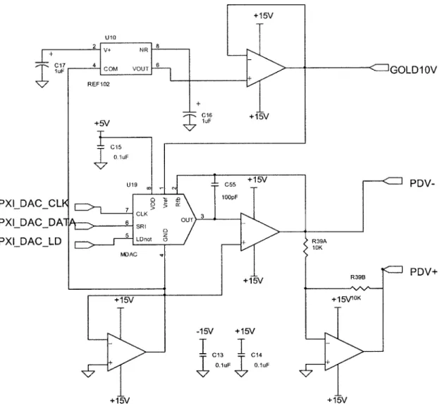
method allows for decoupling of common mode rejection limitations of the DUT from the errors due to gain nonlinearity. This input source is called the Precision Differential Voltage (PDV) generator, and is shown in Figure 15.
PXIDACCL< PXIDAC_DAl PXIDACLD +15V U10 V+ NR+
IuF COM VOUT REF102 C16 +15V +5V T7IuF QZIGOLD10V C15 O.1uF U19 C55 +1PDV-100pF
;CLK
3 t u6 SRIO not R39A' MDAC +15v ~ R39B PV +15V +1 5\/1OK -15V +15V C13 C14 + O.1uF O.1uF +15V +15V3.2.3.3 Grounding Inputs
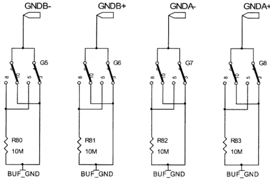
Relays provide the ability to connect each DUT input to the ground signal either directly or through a 1OM9 resistor (resistors R80, R81, R82 and R83 in Figure16). This capability is necessary for performing the VOS, PSRR, IB and IQ tests.
GNDB-G5 R80 10M BUFGND GNDB+ G6 R81 lM 10M BUFGND GNDA-G7 R82 10M BUFGND GNDA+ G8 R83 10M BUFGND
Figure 16. Direct ground paths and resistive paths to the ground signal are available for the inputs of the DUT.
3.2.3.4 DUT Supply Inputs
The DUT is powered through high-voltage high-current op-amp buffers that can be bypassed. A 10M resistor (R17 and R19) in series with each of the DUT power supply pins permits supply current measurement by measuring the voltage drop across the known resistances and applying Ohm's law. The circuit is shown in Figure 17.
+20V C25 + C26 7 U6 e 10uF EXTERNAL VS- IN-IN+ R 'IT Cl)10 OPA547T PXI U8 Enable R205K C27 0.OluF GA s ] DUTVS-1 VlQnegVS-OR - VlQpos_VS-C28 O.1uF -20V 29 1OuF
Figure 17. The DUT power is supplied through a resistor to enable measurement of the current flowing into the DUT supply pins.
3.2.4 DUT Interface
The DUT Interface consists of 16-pin connector in the middle of the INA-TCB, and provides support for the testing of both 8-pin single amplifier ICs and 16-pin dual amplifier ICs. A signal hardwired interface is presented on the INA-TCB, but this can be adapted to suit the pin-out of different instrumentation amplifiers using Socket Adapter Boards.
The DUT Interface consists of ground drivers for the DUT reference pins, gain-resistor connections, load connections, relays for selecting which amplifier channel to apply inputs and measure outputs from and the DUT socket itself. Two loads per amplifier channel are supported. Four gain resistors can be connected to both amplifier channels. The DUT Interface circuitry is shown in Figure 18.
K1 KI 13 14 K1 K1719 20 JP201_GAINGRESISTORS G12 G13 GNDA+ > GNDA- E GNDB+ => GNDB-K K;K K KI K K 0 G10 G11 JP3 G18 G19 kB= K5 K6 PDV- PDV+ SEV= DUTVS+ DUTVS-2 4 6 7 U27 RGB1 R NB-NB+ VO Vs- R SenseA Sen INA- R INA+ VO RGA1 R DUTseat GB2 16 VS+ 15 UTB 14 EFB 13 seB 12 EFA UTA 10 GA2 9 G14 - --- - 8 -5 +15V DUTOUTBUF -1 5V JP201 LOADS +1VR21 R22 +5 L V 00K 100K + -15V -15V BUFGND BUFGND O]DUTREFA ]DUTREFB
Figure 18. The DUT interface connections to multiple inputs, multiple gain-setting resistors, and multiple loads. Support for dual channel amplifier packages is included. Relays are used to swap between the possible configurations.
3.2.5 Output Measurement Circuitry
Relays are used to select the amplifier channel output that the measurements are to be taken from. A pair of 16-input analog multiplexers (muxes), U17 and U18, are used to select the signals to be passed to the measurement amplification stage. The signal
selection is done via digital enable and select signals.
The amplification stage consists of three amplifier options, each with different advantages and limitations. A summing junction amplifier is implemented using the three op-amps U4A, U4B and U4C, and the resistor network consisting of R40A, R40B and R25. This option is used to perform a comparison of two voltages that are supposed to be the same, such as in the gain error test. The comparison is done by applying the two signals with opposite signs, thereby performing an amplification of their difference. The summing junction amplifier is useful for this kind of subtraction because unlike the PGA-based amplifier, it introduces little additional error from its own common mode rejection limitations. The output of the summing junction is then magnified by a known gain factor through the PGA-based amplifier and fed to the digital multimeter.
The PGA-based amplifier is a two-stage amplifier consisting of instrumentation amplifiers with digitally configurable gain that provide good gain accuracy. The first stage is a PGA204 device with gain options of 1, 10, 100 and 1000. The second stage is a
PGA205 device with gain options of 1, 2, 4 and 8. In cascade, they provide gain options of 1, 2, 4, 8, 10, 20, 40, 80, 100, 200, 400, 800, 1000, 2000, 4000, and 8000. Of course,
depending on the initial input signal the output of the amplifier might rail and not provide the expected gain. The PGA-cascade amplifier is used for gaining up small voltages by known factors before measuring with the digital multimeter.
Additionally, a difference amplifier statically configured in a gain of 101 is made available on the INA-TCB measurement path. Due to the high common mode voltage range of the INA145 (U3), it is used for measurements involving signals with high common modes. For example, in the output SWING tests, the DUT output is railed and the voltage obtained is compared with the relevant DUT supply voltage. It is also used in the quiescent current, IQ, tests to measure the potential difference across a known resistance through which the IQ is flowing. In these cases, the summing junction and
PGA-cascade amplifiers do not have large enough common mode voltage ranges to be useful and the difference amplifier is thus used. The circuitry is shown in Figure 19.
R23 MUX A2+ DUTR B BUFGND 1K 100K VIQnsg VS- 23 S4 A2 14 -ing S 2 5 S 3 28 5OIA4 e , MU)~A+ +15V MU)A3+ - -MU)CEN + U1-++10V R4 R2IN A0G406
UT OUT BUF 91
EEN-+20V U UTREF 2 S2 > AO 1G5I UT-REFA 22 3 Al 15 OSng V- 23 S4 A2 14 V QhPeSVS+ 24 6S- INAA3 iQ n eV+ 25 OUT 28 IQ SV+2 S7 OUT OLD1 V 10 2S GND PXG PGA DG 1 _ T __ N- 4S0(~l GOLD S9GND DUT-VS >-115 DGN BUN DGN
Figure 19. The output measurement circuitry includes multiple amplification paths to support
R24 D D D V V V V B G D D OUT1
3.3 DUT Socket Adapters
In order to use the fixed DUT interface available on the INA-TCB, DUT Socket Adapter boards were designed for a number of single and dual channel instrumentation amplifiers. The DUT Socket Adapter implements the rewiring necessary to make the pin-out of a particular instrumentation amplifier conform to the pin-pin-out of the DUT interface on the INA-TCB. Figure 20 shows the Socket Adapter routing for a number of devices that could potentially be tested on the AutoBench system.
Figure 20. A PCB diagram for the DUT socket adapters.
3.4 The Desktop Computer
The desktop computer is the controller for the AutoBench system. The computer provides the processor for executing code. The computer also integrates all the resources,
0-O~ Lu-q * 0 0 *~ 6?~0 0~~ 'IS 0-p V/
stores the data and presents the system's user interface on its monitor. A Pentium 4 based desktop computer running Windows is used for the controller.
The controller computer communicates with the PXI platform resources via a high speed data bus called the MXI-3 link. The MXI-3 link consists of a card that plugs into a hardware slot in the computer frame, a card that plugs into the PXI chassis, and a cable that connects the two systems.