Block Copolymer Self-assembly:
Lithography, Magnetic Fabrication, and Optimization
byKun-Hua Tu
B.S. Materials Science and Engineering, National Taiwan University (2009)
M.S. Materials Science and Engineering, National Taiwan University (2011)
Submitted to the Department of Materials Science and Engineering in partial fulfillment of the requirements for the degree of
Doctor of Philosophy at the
MASSACHUSETTS INSTITUTE OF TECHNOLOGY
September 2017@
Massachusetts Institute of Technology 2017. All rights reserved.A uthor:...
Signature redacted
Department of Materials Science and Engineering
August 18, 2017
S Rinitiirp rP-d],rJt-d
C ertified by: ...
Caroline A. Ross
Toyota Profess
of Materials Science and Engineering
Signature redacted
Thesis Supervisor
Accepted by:...
MASSACHUSETS STITUTE
OF
TEHOOY-OCT 0
4
Z017
Donald R. Sadoway
Chair, Departmental Committee on Graduate StudiesBlock Copolymer Self-assembly:
Lithography, Magnetic Nanofabrication, and Optimization
by
Kun-Hua Tu
Submitted to the Department of Materials Science and Engineering on August 18, 2017, in partial fulfillment of
the requirements for the degree of Doctor of Philosophy
Abstract
Block copolymer (BCP) self-assembly is attractive because it provides nanoscale long-range ordered structures in a massive quantity. The capability of generating features with size as low as 5 nm is of particular interest in semiconductor fabrication since current photolithography has reached its resolution limitation and the other competing technologies are either too slow such as e-beam lithography or too expensive such as EUV system. In this thesis, BCP lithography is utilized to fabricate magnetic nanostructure and the corresponding magnetic properties are explored.
The polystyrene- b-polydimethylsiloxane (PS-b-PDMS) diblock copolymer with different molecule weight is used to generate various sizes of robust silica pattern after solvent annealing and reactive ion etching. Pattern transfer methods are developed to convert the silica pattern into functional materials, including magnetic materials like cobalt, Co/Pd, FePt and CoFeB magnetic tunnel junctions
(MTJ), and MoS2 monolayers. For magnetic nanowire arrays, the interactions
between neighboring wires are investigated. For perpendicular MTJ nanopillar arrays, the size-dependent switching behavior and magnetostatic effects between two layers are analyzed. MoS2 monolayers are patterned into features such as
nanodots, nanorods and nanomeshs and the corresponding photoluminescence are characterized.
Finally, machine learning and deep learning algorithms are the first-time ever demonstrated to model the BCP self-assembly process. The built model is able to recognize different BCP patterns and predicting the resulting morphology and pattern quality based on experimental process parameters. With this model, the BCP self-assembly can be further optimized toward industrial-grade production.
Thesis Supervisor: Caroline A. Ross
Acknowledgements
It is still hard for me to believe that the time has come to the end of my wonderful journey at MIT. It's even harder to for me to imagine where I would be without all the helps along the way. With this chance, I would like to express my deepest gratitude to all of my colleagues, collaborators, friends and families.
Thanks, first and foremost to my advisor, Prof. Caroline Ross, who is a role model of scientist for me. I still remember when I was overwhelmed and struggling in my first year at MIT, it was her to be there and help me to get back on track. Since then, she is always offering big help to listen, discuss, and provide insightful guidance whenever I have problems. I have been inspired a lot from her critical thinking, sharp perspective and the relentless effort in research. On the other hand, she is also an incredible mentor. Her patience, respect and encouraging attitude not only make me feel pumped all the time, but also make the atmosphere in our group extremely enjoyable. It is my privilege to be in Caroline's group and I really appreciate all the things she has brought to my life.
I would like to thank the members of my thesis committee, Prof. Alfredo
Alexander-Katz and Prof. Geoffrey Beach. It is my great pleasure to work with two experts in different areas at the same time. They always give me wise opinions and good directions that sharpen my research. I appreciate the collaborations with Prof. Avgeropoulos, Prof. Wang and Prof. Warner, who provide me the resources that make my project possible. Moreover, I would also like to thank my collaborators, Dr. Pin Ho, Dr. Grace Han, Dr. Larysa Tryputen, Dr. David Navas, Liu Song and Tao Liu, for the invaluable input to my studies. Without you, things would not have gone so smoothly.
I would like to thank all of the members in Caroline's group. I really
appreciate many great help from Wubin Bai, Jean Anne Incorvia, kevin Gotrik and Jinshuo Zhang during my early stage. Without these, my journey would be much tougher than it was. I also want to say thank you to all the other members. All of you have made the group such a warm and joyful place to stay. I would like to extend my gratefulness to the members in the block copolymer sub-group for sharing the knowledge and precious experience in self-assembly. I also appreciate the efforts of James Daley, Mark Mondol, Libby Shaw and all the staffs in managing the experimental tools. It allows me to accomplish my research without facing many obstacles.
I thank Prof. Chun-Wei Chen, who is my advisor during my studies at
been supportive whenever I need his help. I am also grateful for the fellowship support from Think Global Education Trust in the years from 2014-2016.
I would not be able to survive the graduate study without all of my friends. Shang-Wen Li, Chi Lu, Fang-Yu Liu, Man-Chi Liu and Alina Rwei, it is really my fortune that I can have you to share my life with. Chia-Hao Chuang, Chern Chuang, Shao-Sian Li and Henry Wei, you are like my big brothers that always give me unconditional support and life advice. The Taiwanese student community at MIT, you are like my second home in Boston. I really enjoy the numerous beer and board game nights that filled with tons of happy laughter. I am also glad to have my snowboard crew and softball team here. It is hard to imagine how much boring and monotonous my life would be without them. And Wenting, you accompany me through all of the highs and lows. It is such a warm feeling to know you are always there for me. To all of you, I would like to express my thankfulness for being with me through these years.
Lastly, Mom, Dad, and my families, I love you. You are the most important reason for me being here. Although we are 7,800 miles away, your love and care is my strongest backing along the way. I cannot be luckier to grow in such a lovely family. To you, I would never be able to return, all I can do is to say thank you from my deepest heart.
Table of Contents
CHAPTER 1 Introduction ... 25
1.1 Motivation and Thesis Overview ... 25
1.2 Block Copolymer Lithography ... 28
1.2.1 Self-assembly Behavior... 28
1.2.2 Pattern Transfer Methods... 32
1.3 Properties and Applications of Magnetic Nanostructures... 35
1.3.1 M agnetic N anow ires ... 35
1.3.2 M agnetic N anodots ... 40
1.4 Machine Learning and Deep Learning Techniques for Analysis of BCP Self-a ssem b ly ... 4 3 1.4.1 Artificial Neural Networks ... 44
1.4 .2 R eg ression ... . . 48
1 .5 S u m m a ry ... 4 9 CHAPTER 2 Research M ethods ... 57
2.1 Polymers and Spin-coating ... 57
2.2 Solvent-vapor Annealing ... 58
2.3 Etching and Pattern Transfer... 60
2.4 Vibrating Sample Magnetometer (VSM) ... 61
2.5 Alternating Gradient Magnetometer (AGM)...62
2.6 Magnetic Force Microscopy (MFM) ... 63
2 .7 O O M M F ... 64
CHAPTER 3 Universal Pattern Transfer Methods for Metal Nanostructures by Block Copolymer Lithography ... 67
3 .1 In tro d u ctio n ... 6 7 3 .2 E x p erim en tal... 70
3.3 Damascene Pattern Transfer Process... 73
3 .4 L ift-off p rocess ... 76
3.5 Ion-beam E tch P rocess... 78
3.6 Structural Properties of Transferred Pattern...83
3 .8 C on clu sion ... 89
CHAPTER 4 Magnetic Configuration and Interactions in 40 nm W ide Nanowires M ade using BCP Lithography...99
4 .1 In trod u ction ... 99
4.2 Domain Wall Structure and Interactions in Cobalt Nanowires ... 102
4.2.1 E x perim ental... 102
4.2.2 R esults and D iscussion ... 103
4.3 Domain Configurations in Nanowire Arrays with Perpendicular Magnetic A n iso tro p y ... 1 19 4.3 .1 E x perim ental... 119
4.3.2 R esults and D iscussion ... 121
4 .4 C on clu sion ... 138
CHAPTER 5 Magnetic Reversal and Thermal Stability of BCP-patterned CoFeB Perpendicular Magnetic Nanopillar Arrays ... 149
5 .1 In trod u ction ... 149
5 .2 E x perim en tal... 15 1 5.3 Size-dependent Switching Behavior and The Effects of Magnetostatic Interactions ... 1 5 4 5 .4 C on clu sion ... 169
CHAPTER 6 Application of Block Copolymer Patterning for Two-Dimensional M aterials ... 175
6 .1 In trod u ction ... 175
6 .2 E xp erim en tal... 177
6.3 Nanopatterning of Photoluminescent MoS2 Monolayer ... 179
6.4 Enhanced Mobility in MoS2 Field-effect Transistor with BCP Patterned S u b strate ... 19 6 6 .5 C on clu sion ... 199
CHAPTER 7 Modeling and Optimization of Block Copolymer Self-assembly using M achine Learning ... 211
7 .1 In trod u ction ... 2 11
7.3 Block Copolymer Pattern Recognition... 215 7.4 M odeling of Self-assembly Process and Pattern Prediction ... 219 7.5 Line Array Quality Prediction... 227 7 .6 C o n clu sio n ... 2 32
CHAPTER 8 Summary and Future Work...237
8 .1 S u m m a ry ... 23 7 8 .2 F u tu re W o rk ... 239
List of Figures
Figure 1-1 The schematic of a linear diblock copolymer and its potential bulk m orphologies [22] ... 29
Figure 1-2 Phase diagrams of the bulk morphology in diblock copolymer system which is (a) predicted by SCFT, (b) obtained experimentally. (S: sphere, C: cylinder, L: lamellae, PL: preforated lamellae, G: gyroid,
CPS: close-packed sphere) [23]. ... 31
Figure 1-3 Thin film morphologies of diblock copolymer. (a) spheres (b) cylinders (c) perforated lam ellae ... 32
Figure 1-4 The schematic of the fabrication process of the cobalt dot array via block copolymer lithography [32]... 34 Figure 1-5 (a) The schematic structure of Bloch wall and Neel wall. (b) The total energy of Bloch and N&l wall with different film thickness (top). As the system favors the configuration with lower energy, Nel wall is dominated when the film is thinner than 40 nm while the Bloch wall is preferred when the film is thicker than 40 nm. The bottom diagram shows the DW width as a function of film thickness [45]. ... 36 Figure 1-6 Magnetic configuration of (a) transverse wall and (b) vortex wall in thin film wire. (c) Phase diagram of transverse wall and vortex wall under different thin film width and thickness [46]... 37
Figure 1-7 (a) Example of magnetic domain wall logic circuit. The DW is driven
by a rotating magnetic field and the results are measured by MOKE
at position 1, 11, 111 and IV [17]. ... 38
Figure 1-8 The schematic of racetrack memories with different implementations [8].
... . . . 4 0
Figure 1-9 (a) Schematic single domain magnetic particle system and (b) the predicted hysteresis loops of Stoner-Wohlfarth model [49]... 41 Figure 1-10 Schematic of the storages in HDD and bit patterned media [53]... 43 Figure 1-11 Schematic architecture of a feedforward neural network with two hidden layers. (b) The calculations of each node in the network and the analogy to the neuron in biological brain. (picture credit: Stanford C S231n w ebsite) ... 45 Figure 1-12 (a) Illustration of the functionality of a maxpooling layer. (picture credit: Stanford CS231n website) (b) A schematic example of the
architecture of a convolutional neural network. (picture credit: W ILD M L w ebsite)... 47 Figure 1-13 Schematic of a recurrent neural network. (picture credit: colah's blog)
... . . 4 8
Figure 2-1 Schematic of solvent-vapor annealing process and setup. The graph on the top right corner shows an example of the thickness of a swelled B C P film over tim e... 59
Figure 2-2 Schematic of vibrating sample magnetometer. (picture credit: W ikipedia)... 62
Figure 2-3 Schematic of alternating gradient magnetometer [6]... 63
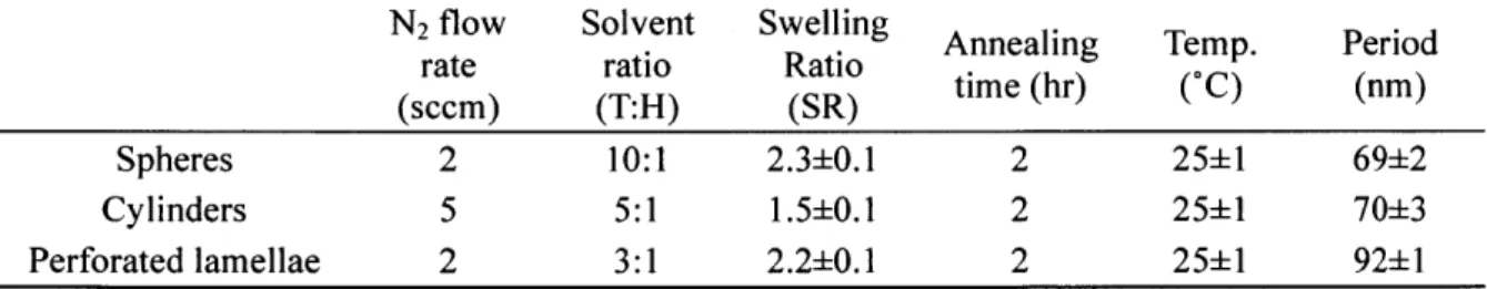
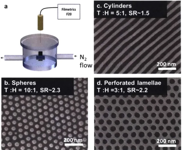
Figure 3-1 (a) Glass annealing chamber with nitrogen inlet and outlet to control the vapor pressure during solvent vapor annealing. The BCP film thickness is tracked by spectral reflectometry with the light transmitted through the quartz lid. (b)-(d) Representative SEM images of oxidized PDMS nanostructures formed from 42 nm thick SD75 thin films with different solvent annealing conditions listed in Table 1. T:H is toluene:heptane volumetric ratio and SR is swelling ratio... 73 Figure 3-2 Schematic of Damascene-like pattern transfer process from BCP to m etal nanostructures. ... 74 Figure 3-3 Representative SEM images of cobalt films at different times during CF4
reactive-ion etch. The sputtered cobalt film was planarized after 25 minutes etch. At 38 min the oxidized-PDMS had been fully removed and longer etch times caused shrinkage of the Co features. (a) cobalt nanowires transferred from a SD75 cylinder structure. (b) cobalt nanodots transferred from a SD75 perforated lamella structure... 75 Figure 3-4 Resistance of a cobalt film as a function of CF4 reactive-ion etch time,
measured with two-point probes placed 5 mm apart. It increased dramatically when the film was no longer continuous, indicating the com pletion of etching... 75
Figure 3-5 Schematic of liftoff pattern transfer process from a BCP mask using a sacrificial PM M A underlayer ... 78
Figure 3-6 SEM images of cobalt nanodots and nanowires fabricated by lift-off process. The inset tilted views illustrate edge tapering. ... 78 Figure 3-7 Schematic of subtractive pattern transfer process from BCP self-assembled mask by reverse transfer ion-beam etch process. ... 80
Figure 3-8 Plane view and cross-sectional SEM images at different stages during the ion-beam etch process. (a)-(c) show the transfer of a perforated lamellae pattern and (d)-(f) show the transfer of a cylinder pattern.81 Figure 3-9 Schematic of direct transfer ion-beam etch process... 82
Figure 3-10 (a)-(c) Plane-view and cross-sectional SEM image of carbon hard mask. (a) Cylinder pattern. (b) (c) sphere pattern. (d) (e) The cobalt nanowire patterned with direct transfer ion-beam etch process... 82 Figure 3-11 In plane hysteresis loops of cobalt nanodots patterned by three different processes compared to an unpatterned film... 88
Figure 3-12 The surface topography of ion beam patterned (a) cobalt nanodots and (c) nanowires imaged by scanning probe microscopy. (b)(d) The corresponding magnetic structure of the morphologies in (a) and (c).
... . . 8 8
Figure 4-1 (a) Scanning electron microscopy image of BCP patterned cobalt nanowire arrays, in which the dashed boxes indicate examples of typical defects including 1. Y-junction, 2. T-junction, and 3. line termination. Inset shows a tilted cross-sectional image of the wires. Cobalt nanowire arrays after (b) DC-remanence, and (c) AC-demagnetization. The magnetic force contrast was superposed on the topographic image for clarity. Red and blue show where stray field is present. DWs with the same sense repel, as shown in the dashed box of (b), while DWs with the opposite sense were attracted, as shown in the dashed box of (c)... 106
Figure 4-2 (a) The magnetization of a head-to-head transverse domain wall in a cobalt nanowire simulated by OOMMF. Wire dimensions: 1000 nm long x 40 nm wide x 20 nm thick. (b) The z-component of the stray field produced by (a) in a plane 10 nm above the wire. (c) The y-component of the stray field in a plane at half the wire height. (d) Magnetic field amplitude of (c), which was acquired along the line through the center of the DW. (e) Enlarged section of (d) around y
7 0 n m ... 10 7
Figure 4-3 (a) The magnetization of a tail-to-tail DW in 40 nm wide cobalt nanowire. (b) The corresponding stray field in the z-direction in a plane
Figure 4-4 Schematic of the magnetic configurations of two transverse DWs in adjacent wires. The uppercase letters correspond to the cases listed in T a b le 1 ... 10 9
Figure 4-5 OOMMF simulations of DW interactions in two parallel wires. (a) two identical head-to-head DWs were initialized in the middle of the wire (case A in Table 1), and moved apart within 100 ns. (b) one tail-to-tail and one head-to-head DW (case C in Table 1) were initialized with an offset of 1000 nm, and the two DWs were attracted towards each o th er. ... 1 10
Figure 4-6 (a) A tail-to-tail and a head-to-head DW (case "C" of Table 1) were initialized in the middle of two nanowires with the core magnetization aligned in the same direction. After 150 ns evolution the walls remained together at the same place. (b) Two identical head-to-head DWs (case
"A" of Table 1) were initialized with a spacing of 10 nm, and stayed
together after 150 ns relaxation... 111
Figure 4-7 The simulation of DW interactions in a multi-wire system. Wire dimensions were 2 vm (L) x 40 nm (W) x 20 nm (H), with periodicity
70 nm. (a) 2 wires, (b) 3 wires, (c) 4 wires, (d) 5 wires. The DWs have
the same structure in each wire (case A of Table 1). In each case the DWs repelled each other and moved apart in opposite directions. When there was an odd number of wires, one of the wires stayed at the center of the nanow ire... 112 Figure 4-8 Five nanowires were built with tapered edge with the cross-sectional image shown underneath. Head-to-head DWs were initialized in the middle of the wire, and after 100 ns evolution, they repelled each other, giving similar results as in figure 4-7(d). ... 113
Figure 4-9 OOMMF simulation of DW behavior under an applied field in the
+x
direction. (a) The initial magnetization of one HH DW in the top wire and one TT DW in the bottom wire, with their DW dipoles aligned in the
+y
direction, corresponding to case "C" described in Table 1. (b) After applying a field in the +x direction for 150 ns, the DWs could only be separated by a field larger than 455 Oe. (c) The initial magnetization of one HH DW in the top wire and one TT DW in the bottom wire, with their DW dipoles aligned in the -y direction, corresponding to case "F". (d) After applying a field in the +x direction for 150 ns, the DWs could only be separated by a field larger than 73 O e .. ... 1 15Figure 4-10
Figure 4-11
Figure 4-12
Figure 4-13
Mapping of the magnetostatic interactions between two identical DWs in parallel wires with width of (a) 40 nm (b) 80 nm (c) 120 nm (d) 160 nm as a function of wire spacing and thickness. The solid star in (a) shows the geometry of the actual sample. The repulsive behavior agrees with our experimental observation at DC-remanent state... 116 (a)-(c) The magnetization of head-to-head DWs in cobalt wires with different widths. Wire dimension: 2 jim (L) x (a) 40 nm, (b) 80 nm, (c)
160 nm (W) x 5 nm (H). The images shown here are not to the same
scale. (d)-(f) the corresponding stray field in the y-direction of the DWs in (a)-(c) respectively... 117
Stray fields originating from nanowire junctions. (a)-(d) T-junction in a cobalt nanowire. (a) and (b) are the AFM and MFM images at DC-remanence respectively. In (b) an asymmetrical dark contrast was observed at the bottom left side of the junction. (c) the magnetization inside the T-junction simulated by OOMMF. The T-shape junction was modeled with a wire width of 40 nm, thickness of 20 nm, and initial magnetization pointing to the right and upwards. After 10 ns relaxation, the configuration consisted of the lower wire magnetized to
the right and the middle wire magnetized upwards. (d) the
corresponding stray field of (c) in the z-direction 10 nm above the wire, which qualitatively matches the MFM image of (b). (e)-(h) Y-junction in a cobalt nanowire. (e) and (f) are the AFM and MFM images respectively. (c) the magnetization inside the Y-junction simulated by OOMMF. (d) the corresponding stray field of (g) in the z-direction 10 nm above the wire. The stray field gave a good agreement with the M F M ... 1 18
Plane-view HIM images showing (a) BCP patterns on SiO2/[Co/Pd]15 and (b) BCP patterns on MgO/Llo-FePt. Inset of (b) shows a double layer BCP lamellar structure. (c) Co/Pd nanowires after pattern transfer. Inset of (c) shows a cross-sectional HIM image of the tapered Co/Pd nanowires. (d) Llo-FePt nanowires and other structures after pattern transfer. (e) Cross-sectional TEM image of BCP patterned Co/Pd nanowires. Inset shows the polycrystalline lattice of a Co/Pd nanowire, where the grain boundary is depicted by white symbols. (prepared by C ongli) ... 123
Figure 4-14
Figure 4-15
XRD spectrum of (a) Co/Pd before and after BCP patterning (b) Llo-FePt before and after BCP patterning. The unlabelled sharp peaks in
(b) are inherent to the MgO substrate. (prepared by Hopin)... 124
Hysteresis loop of (a) unpatterned SiO2/[Co/Pd]1 thin film, (b) BCP
patterned array of Co/Pd nanowires, (c) unpatterned MgO/Llo-FePt (20 nm) thin film. Inset shows the XRD spectrum of the L1o-FePt before and after BCP patterning. The unlabelled sharp peaks originate from the MgO substrate. (d) BCP patterned array of Llo-FePt nanowires. (prepared by Hopin) ... 127
Figure 4-16 OOMMF simulations. In each case red and blue represent the component of magnetization out of the film plane and the arrows show magnetization vectors. (a) 3D schematic of a Co/Pd Noel DW and the magnitude of dipolar stray field experienced at the edge and centre of the Co/Pd nanowire from its two nearest neighbors. (b) Plan-view of three Co/Pd nanowires, with a Neel DW in the center nanowire, and the outer nanowires magnetized 'up' (red). (c) Propagation of the 'down' domain (blue) by Nel DW motion to the left in the center Co/Pd nanowire driven by the stray field from its neighbors. (d) 3D schematic of a L1o-FePt Bloch DW and the magnitude of dipolar stray field experienced at the edge and centre of the LIo-FePt nanowire from its two nearest neighbors. (e) Plan-view of three Llo-FePt nanowires, with a Bloch DW in the center nanowire, and the outer nanowires magnetized 'up' (red). (f) Propagation of the 'down' domain (blue) by Bloch DW motion to the left in the center LIo-FePt nanowire driven
by the stray field from its neighbors. (prepared by Jinshuo)... 128
Figure 4-17 (a) AFM (left) and MFM (right) images of BCP patterned Co/Pd nanowires after AC demagnetization. (b-e) MFM images of Co/Pd nanowires at remanence after applying a field of H, = (b) -500, (c)
-1000, (d) -1500 and (e) -2000 Oe. (f) AFM (left) and MFM (right)
images of unpatterned Co/Pd thin film after ac-demagnetization. (g-j) MFM images of unpatterned Co/Pd thin film at remanence after applying a field of Hz = (g) -500, (h) -1500, (i) -3000 and (j) -4000 Oe.
All MFM images are captured at a fixed location on the patterned and
unpatterned Co/Pd. Red and yellow contrast in the MFM images indicate 'up' and 'down' stray fields, respectively. (prepared by Hopin)
Figure 4-18 (a,b) 3D diagram showing the magnetic information (MFM) superimposed on the topography (AFM) of the ac-demagnetized (a) Co/Pd and (b) Llo-FePt nanowires. Blue and red shading indicate 'up' and 'down' magnetization, respectively. (c,d) Area fraction of reversed domains versus applied reversed field as a percentage of saturation field for unpatterned and BCP patterned films of (c) Co/Pd and (d) Llo-FePt. The dashed lines serve as a guide for the eye. The saturation field is taken to be the field at which the out-of-plane hysteresis loop closes. Saturation fields of the unpatterned Co/Pd, Co/Pd nanowires, unpatterned FePt film and FePt nanowires are 4.8, 3.2, 8.8, and 10.0 kOe, respectively. (prepared by Hopin)... 133
Figure 4-19 (a) AFM (left) and MFM (right) images of BCP patterned Llo-FePt nanowires after ac-demagnetization. MFM images with applied field of
Hz = (b) -2, (c) -4, (d) -6, (e) -8 kOe, captured at a fixed location on
the sample. MFM images of unpatterned Llo-FePt after (f) ac-demagnetization and (g) applied field of H, = -6 kOe. Red and yellow contrast in the MFM images indicate 'up' and 'down' magnetization, respectively. (prepared by Hopin)... 137
Figure 4-20 MFM images of unpatterned Llo-FePt (a) after ac-demagnetization and (b-d) at remanence after an applied field of Hz = (b) -2, (c) -4, and (d) -6 kOe. Red and yellow contrast in the MFM images indicate 'up' and 'down' magnetization, with the red domains favored by the negative applied field. (prepared by Hopin) ... 138
Figure 5-1 (a) A schematic of the layered structure of the perpendicular magnetic tunnel junction used in this work. (b)(c) Block copolymer patterning process for magnetic nanostructure. In (b) the perforated lamellar BCP pattern is transferred to the magnetic thin film with inverse contrast, while in (c) the sphere BCP pattern is transferred directly... 153 Figure 5-2 (a)(c) Scanning electron microscope images of patterned p-MTJ nanopillars. The inset in (a) shows the perforated lamellae BCP pattern used for inverse transfer method. (b)(d) The distribution of pillar diameters in (a) and (c) respectively... 156
Figure 5-3 (a) In-plane and out-of-plane hysteresis loop of unpatterned p-MTJ thin
film, showing perpendicular magnetic anisotropy. (b) Out-of-plane
hysteresis loops of p-MTJ nanopillars with diameter of 64 and 25 nm. The sample of 64 nm pillars showed a smaller magnetic moment because of the presence of regions without dots. ... 157
Figure 5-4 (a) First-order reversal curves of 64 nm p-MTJ pillars, showing only
1/10 of all the measured curves for clarity. (b) The corresponding
FORC distribution. The color represents the value obtained from equation 1. (c) Schematics of the magnetic configuration of patterned nanopillar arrays. The numbers represent different configurations in (a )... 1 5 9
Figure 5-5 Magnetic force microscope images of 64 nm p-MTJ pillars. The field of view is 1pm x 1pm. (a)-(f) Images taken at remanence after saturating then applying different reverse fields. (d,e) show clear evidence of coexisting up and down net magnetic moment... 161
Figure 5-6 (a) First-order reversal curves of 25 nm p-MTJ pillars, showing only
1/10 of the measured curves for clarity. (b) The corresponding FORC
distribution of (a). ... 162
Figure 5-7 Calculated out-of-plane magnetostatic field distribution of (a) the hard layer at the midline position of the soft layer and (b) the soft layer at the midline position of the hard layer... 163
Figure 5-8 The hysteresis loops of (a) 64 nm and (c) 25 nm nanopillar arrays measured under different field sweeping rate. (b)(d) The linear fitting of the variation of coercivity with respect to log of the scan time t (inversely proportional to the field sweep rate), from which the thermal stability factor and Ho are obtained using eq. 8. ... 167
Figure 5-9 In-plane and out-of-plane hysteresis loops of (a) 64 nm pillar and (b) 25 nm pillar arrays. ... 168
Figure 6-1
Figure 6-2
Schematic illustration of the BCP patterning process for nanodot fabrication in MoS2. a) Flow chart for nano-patterning procedure of
monolayer MoS2 domains using PS-b-PDMS block copolymers as an
etch mask. Schematics of b) monolayer MoS2 patterned in the shape
of dots and c) an array of nanodots (~20 nm in diameter) formed as a result of B C P lithography... 180 SEM characterization of the nano-patterned MoS2 fabricated by BCP
and oxygen plasma etching. a) SEM image of the as-grown MoS2 before
BCP patterning. b) SEM image showing a large area of the sample covered with silica-like ox-PDMS nano-structures after oxygen plasma etching of BCP patterns. c) SEM image of a single triangular MoS2
domain with ox-PDMS pattern. The dark micron-scale patterns represent the areas covered with ox-PDMS rods that are generated by
Figure 6-3
Figure 6-4
Figure 6-5
the BCP bilayer. Lighter regions are covered with ox-PDMS dots that are formed by the BCP monolayer. d) SEM image with higher magnification showing the edges of MoS2 domains (dark contrast) with
the ox-PDMS mask covering the entire substrate. e) SEM image of the detailed structure of the ox-PDMS mask on MoS2, showing the
presence of well-ordered dot and rod arrays (light contrast). f) Magnified view of the region indicated with the red box in e) showing hexagonally packed ox-PDMS dots and the line profile of dots. g) Magnified view of the region indicated with the yellow box in e) showing ox-PDMS rods and their line profile. The average diameter or width of dots and rods is 16-20 nm ... 182
Optical microscope and SEM characterization of nano-structured MoS2
after the lift-off process. Optical microscope images of monolayer MoS2
domains that are a) pristine (as-grown), b) covered with an ox-PDMS mask layer, c) nano-patterned mostly with rods after the lift-off process, and d) nano-patterned with dots and rods. e) SEM image of a nano-patterned monolayer MoS2 domain comprised of MoS2 dots and
rods, as the domain in d). f) Magnified view of the region indicated with the red box in e) showing hexagonally packed MoS2 dots and the
line profile of dots. g) Magnified view of the region indicated with the yellow box in e) showing MoS2 rods and their line profile. MoS2 is seen
darker relative to the SiO2 substrate. The average diameter or width
of MoS2 dots and rods is 16-20 nm. h) A domain patterned mainly in
the shape of rods with smaller number of dots filling the space between rods, corresponding to the optical image c). i) Larger area of MoS2 nanodot arrays with a hexagonal order. Bright dots represent ox-PDMS that remained after the lift-off process. (prepared by Grace H a n )... 18 5 SEM images of nano-patterned (a-c) micro- and (d) nano-scale MoS2
domains in the form of nanodots and nanorods. Bright particles are residual oxidized PDMS dots that remained after the lift-off process. (prepared by G race H an)... 186 SEM images of nano-patterned (a-c) micro- and (d) nano-scale MoS2
domains in the form of a hexagonal
nanomesh.
These domains are found near the edge of a substrate where thick layer of BCP is deposited. (prepared by Grace Han)... 187Figure 6-6 AFM characterization of nano-structured MoS2 after the lift-off process.
a) Low-magnification AFM topography of nano-patterned monolayer
MoS2. b) Representative mid-magnification topography of the outlined
area in a) (green) in the center of the MoS2 domain. c) Height profile
of the denoted section (blue line) in a) showing a monolayer thickness
of MoS2 on the SiO2 substrate. d) Magnified view of the region
indicated with the red box in b) showing nanodots. e) Magnified view of the region indicated with the yellow box in b) showing nanorods. f) Representative high-resolution topography of the outlined area in a) (white) near the edge of the MoS2 domain, showing individual MoS2
dots and rods. Height profiles from the respective red and yellow lines indicated in f) for g) nanodots and h) nanorods. The average height of
~1 nm corresponds to a monolayer thickness, and the average size of
the nano-patterns of 16-20 nm matches the SEM characterization. (prepared by G race H an)... 189
Figure 6-7 AFM topography of (a) nano-scale domains patterned into dots and rods, (b-c) a micro-scale domain where dots are connected to form rods, and (d) a domain that is mainly patterned into nanomesh due to the thick BCP deposition. (prepared by Grace Han)... 190
Figure 6-8 Optical property changes of MoS2 domains induced by nano-patterning.
Normalized photoluminescence (PL) a) and Raman b) spectra of monolayer MoS2 nanodots and nanorods before the lift-off process
(under an ox-PDMS mask after 02 plasma etching) and those of pristine MoS2 shown for comparison. Normalized PL c) and Raman d)
spectra of mionolayer MoS2 nanodots and nanorods after the lift-off
process and those of as-grown MoS2 domains included for comparison.
The Raman spectra of pristine domains transferred onto another SiO2
substrate exhibits similar shifts of both E 12g and Aig modes to those of nano-patterns. e) Relative PL of nano-patterned and pristine domains after the lift-off process (identical data as shown in c), normalized to the Raman Aig intensity). f) Plot of the relative PL as a function of the E/A ratio for the 4 different types of MoS2. PL are all normalized
to the Raman Aig peak. (prepared by Grace Han)... 193
Figure 6-9 SEM images of nano-patterned MoS2 domains with preferentially
remaining nanorods and hexagonal mesh patterns after a long lift-off process (24 h in an acetone bath). Nanodots are loosely bound to the SiO2 substrate and have a strong interaction with the PMMA layer, so
etched triangular MoS2 domains. (b) Magnified view of the
nanorod/mesh region and mostly empty dot area. (c) Magnified view of nanorods and partially remaining dots between the rod patterns. (d) Nanorod/mesh patterns with partially empty spots that have lost nanodot flakes...195 Figure 6-10 Substrate morphology dependence of MoS2 FETs. a. Relationship
between average FET mobility and substrate RMS roughness. The dielectric environment has no measurable effects on FET mobility. b. Statistical distribution of MoS2 FET mobility on selected substrates.
(prepared by T ao and Liu)... 197
Figure 6-11 Pre-pattering method for improvement of FET performance on Si02
substrate. a. Schematic illustration of Si02 patterning using self-assemble polymer. b. SEM image of patterned etching mask and AFM image of resulted c-Si02 after etching. Scale bars are 250 nm. c. Distribution of MoS2 mobilities measured for c-Si02 devices. (prepared
by T ao and L iu) ... 197
Figure 6-12 Statistical distribution of MoS2 FET mobility on Si02 substrate.
(prepared by Tao and Liu) ... 198
Figure 6-13 Raman spectra of MoS2 on Si02 and c-SiNx substrates. Both samples
have same thickness. Peak softening is observed for c-SiNk supported sam ple. (prepared by Tao and Liu)... 199
Figure 7-1 (a) The apparatus for solvent vapor annealing of BCP thin film. The swelling film thickness is in-situ monitored by spectral reflectometer.
(b)-(e) Morphologies of (b) spheres, (c) single layer cylinders, (d) double layer cylinders and (e) a mixture of three patterns generated
by PS37-b-PDMSi6 under different solvent annealing condition... 214
Figure 7-2 (a) Example images of three BCP patterns in pattern recognition task. Top row: spheres. Second row: single layer cylinders. Third row: double layer cylinders. The images here are in different in scale, feature size and orientation as we want to mimic the practical situation and make the model more robust. (b) The data distributions of each pattern in the train, validation, and test data set... 216
Figure 7-3 Schematic of the architecture of convolutional neural network used for B C P pattern recognition... 217
Figure 7-4 The (a) categorical cross-entropy loss and (b) prediction accuracy of the train and validation data set in the training stage of CNN for BCP
pattern recognition task. The accuracy has reached nearly 100% after training for 6 epochs. ... 218
Figure 7-5 The (a) KL divergence loss, (b) average proportion error and (c) prediction accuracy of the train and validation data set in the training stage of FNN for morphology prediction task... 222 Figure 7-6 The swelling BCP film thickness monitored by spectral reflectometer during annealing. The number in parenthesis represents the areal percentage of each pattern...223 Figure 7-7 The (a) KL divergence loss, (b) average proportion error and (c)
prediction accuracy of the train and validation data set in the training stage of CNN for morphology prediction task. ... 223
Figure 7-8 The schematic of the LSTM network (top part) used in morphology prediction task and the using of sliding window method (not to scale) to feed data into the network. ... 224 Figure 7-9 The (a) KL divergence loss, (b) average proportion error and (c) prediction accuracy of the train and validation data set in the training stage of LSTM network for morphology prediction task. ... 225 Figure 7-10 The effects of (a) initial film thickness, (b) maximum swelling ratio, (c) final swelling ratio and (d) time on pattern areal proportion change predicted by feedforward NN... 227
Figure 7-11 Example of characterizing line pattern quality. (a) The original SEM image (b) Image with the defects marked (c) Orientation map (d) The fitting of correlation length, where the raw correlation data is shown in red and the smoothed data is blue. ... 229
Figure 7-12 (a)(c) The comparison of the true value and the model predicted value in defect density and correlation length respectively. (b)(d) The corresponding model coefficient in predicting (b) defect density and (d) correlation length ... 231
List of Tables
Table 3-1 Solvent vapor annealing conditions for three different equilibrium m orphologies of SD 75. ... 72
Table 3-2 Structural characteristics at different stages during patterning. The values were obtained from image analysis of Figure 3-8... 84 Table 4-1 List of 16 possible magnetic configurations of two transverse DWs in adjacent wires. The distinct cases are labeled A-F where in A, D : interactions depend on wire geometry, B : strong repulsion, C : strong
attraction, E : weak repulsion, F : weak attraction. *schematic is provided in figure 4-4...109 Table 5-1 Estimation of the magnetic properties of BCP patterned p-MTJ
n an o p illars... 168
Table 7-1 The process parameters used in training feedforward neural network for morphology prediction and the distribution statistics in the training se t . ... 2 2 1 Table 7-2 The process parameters used in training feedforward neural network for morphology prediction and the distribution statistics in the test set.
... 2 2 1 Table 7-3 Summary of the performance metrics for each model in morphology pred iction task ... 221 Table 7-4 List of the distribution statistics of each pattern quality metric in the
train ing d ata ... ... 229
Table 7-5 List of the distribution statistics of each pattern quality metric in the test d ata ... 229
Table 7-6 Summary of the R2 score of predicting each pattern quality metric by ridge regression m odel. ... 232
CHAPTER 1
Introduction
1.1 Motivation and Thesis Overview
Self-assembly is a special gift of nature that an ensemble of disordered individual components spontaneously forms an organized structure, as a consequence of specific, local interaction among the components. Block copolymer (BCP), as one of the many self-assembly systems, has demonstrated the capability of generating a variety of well-ordered periodic structures at the scale ranging from
5 to 100 nm [1-5]. This is of particular interest in semiconductor industry because the current photolithography has encountered the bottleneck of resolution, and BCP self-assembly is one of the emerging technologies that solves the issue. Some other potential candidates are electron beam (e-beam) lithography and extreme ultraviolet lithography (EUV). Compared with e-beam lithography, BCP self-assembly possess the advantages of high scalability and high throughput, as the pattern for a 300 mm wafer can be done in minutes using BCP self-assembly while it would take up to years by e-beam system depending on resolution, feature size, dose and beam current. On the other hand, although EUV has the most similar working mechanism as photolithography that guarantees the throughput and the integration to the production line, the cost of EUV tools is enormous. A single
the current system, not mentioning billions of dollars spent in developing. By contrast, BCP itself is inexpensive, and because of the simple processing, the required apparatus is much more cost-effective.
As the BCP self-assembly provides the desired pattern, transfer methods are also required in order to convert the BCP morphology to functional materials. In chapter 3, three pattern transfer methods have been developed for
polystyrene-block-polydimethylsiloxane (PS-b-PDMS) diblock copolymer, including the
Damascene, liftoff and ion-beam etch process. Magnetic nanowires and nanodots were demonstrated with these pattern transfer processes and compared in term of structural and magnetic properties.
Magnetic based devices have been an important part for information storage and sensing in consumer electronic industry for decades. Although having the benefits of high capacity, high reliability and low fabrication cost, they suffer from the low energy efficiency and low processing speed. The recent development in spintronics [6, 7], a portmanteau meaning of spin transport electronics, has not only addressed these issues but further exhibited the potential ability in logic. For example, the prototypes of racetrack memory [8, 9] and magnetic random access memory [10-13] have shown the promising writing and read performance with low energy consumption at the order of 100 femto-Joule [14, 15]. Domain wall based devices were demonstrated to perform gate-like functionality and logic computing.
[16-18] In these applications, the fabrication of magnetic nanodots and nanowires
are necessary. Nevertheless, because of the limitations in lithography, large-area, high density arrays of device in nanoscale size were usually difficult to obtain, and thus BCP self-assembly has become a great tool to fill the gap. This also enables the collective characterization of magnetic properties using magnetometry, such as alternating gradient magnetometer and vibrating sample magnetometer. In chapter
4, the high-density arrays of magnetic nanowires with in-plane and out-of-plane anisotropy are realized using BCP lithography. The size-dependent interactions between adjacent nanowires are analyzed and reported. In chapter 5, magnetic tunnel junction nanopillar arrays with the diameter of 25 nm and 64 nm are patterned with BCP lithography, and the reversal behavior and thermal stability are studied in detail.
2D materials (single layer materials) is another potential candidate to be
used in future electronics. Since being discovered in 2004 [19], graphene has attracted extreme large attention because of its extraordinary intrinsic material properties. For example, it has the known highest carrier mobility of 200,000 cm 2V- s- , which is about 400 times higher than silicon. Moreover, the thermal
conductivity and mechanical strength are also the highest among other materials to date. Other 2D materials are of interest as well since they may obtain comparable properties as graphene but with an existing bandgap, making them more suitable for electronic application. BCP self-assembly is incorporated here to adjust the properties of 2D materials. In chapter 6, we show the changing in photoluminescent characteristics of nanopatterned molybdenum disulfide (MoS2)
monolayer. Its carrier mobility can also be enhanced using crested substrate patterned by BCP lithography.
Although BCP self-assembly is promising in lithographic application, a few problems remain to be conquered in order to transit the laboratory demonstration into industrial production. One of them is high defect density. Intrinsic BCP
morphology tends to have defects as the randomness is inevitable in
thermodynamically-driven self-assembly. The other issues in long-range order, edge roughness and uniformity are also critical. Thus, finding an optimal self-assembly process condition that results into low defect, long-range order pattern is
important. Researchers have been using theories like thermodynamic and polymer kinetics to understand the self-assembling behavior, and developed self-consistent field theory (SCFT) to simulate the BCP evolution [201. However, the gap between theory and practical experiment still exists, and it is infeasible and inefficient to experiment all the potential combination of process parameters to find the optimal condition. In chapter 7, a pioneering approach, machine learning and deep learning, has been utilized to model the BCP self-assembly process. The resulting BCP morphology and pattern quality can be predicted by the machine learning model with given process parameters and the optimal condition can be found by grid searching through the parameter space. Moreover, the potential physical relationship between the process parameters and results would be able to inferred from the modeling.
In the last chapter of the thesis, the works in exploring block copolymer self-assembly are summarized, including developing pattern transfer methods, the applications in magnetic nanodevice and 2D materials, and the self-assembly process optimization. A few suggestions for the future work are provided at the end.
1.2 Block Copolymer Lithography 1.2.1 Self-assembly Behavior
Block copolymers (BCPs) are a class of polymers that two or more distinct polymer chains are connected together by covalent bond [21]. If the polymer chains are immiscible to each other, phase separation is desired at the temperature below the order-disorder transition temperature. Macro scale phase separation is prohibited as the polymer chains are still bonded together; instead, BCP will self-assemble into periodic structures as the microphase separation happens [21]. For a
diblock copolymer, which has two different polymer chains linearly bonded together, several bulk morphologies are available, including spheres, cylinders, gyroid and lamellae. Figure 1-1 shows the schematic of a diblock copolymer and the potential bulk morphologies.
A B
spheres cylinders gyroid lamellae gyroid cylinders spheres
Figure 1-1 The schematic morphologies [22].
of a linear diblock copolymer and its potential bulk
Flory-Huggins model is used to understand the thermodynamic driving forces that cause the spontaneous BCP phase separation. In this model, the change in Gibbs free energy of mixing two dissimilar polymers is given by
AGmix f f
where
f
is the volume fraction, N is the repeat units of each polymer, X is the Flory-Huggins interaction parameter, kb is the Boltzmann constant and T is the absolute temperature. As the universe tends to minimize the free energy, if the change in the energy term is greater than zero, the mixing these two polymers is unfavorable, and therefore the spontaneous phase separation happens. The Flory-Huggins parameter here describes the dissimilarity between two chemistries and is formulated asVseg (SA - 5B)2
X RT
where Vseg is the actual volume of a polymer segment, 6 is the Hildebrand solubility parameters and R is the gas constant. In practice, the product XN is used to estimate the segregation strength of two polymer blocks. If XN < 10 (as f=0.5 in the bulk system), two polymer chains would be intermixed and shows a disordered morphology, and if XN
>>
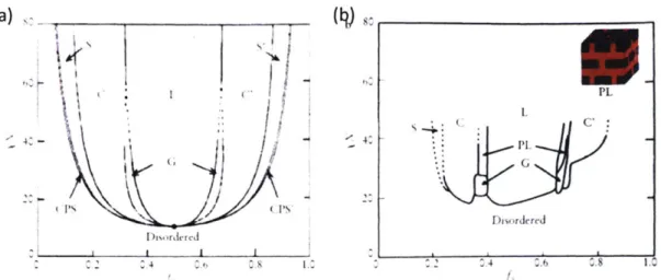
10, there would be a strong segregation force and theinterphase region between two polymers would be narrow. If XN-10, which is around weak segregation limit, the two polymers would be slightly mixed at the interface and the composition profile would be sinusoidal [211. According to this rule, if one would like to obtain the structure of small feature size (small N) using diblock copolymer, selecting the two polymer blocks with a high Flory-Huggins parameter is required. Figure 1-2 shows the phase diagram of diblock copolymer morphology under different XN and fA, as (a) is predicted by self-consistent mean-field theory (SCFT) and (b) is the experimental result from poly(isoprene-styrene) diblock copolymer system. The discrepancy between the numerical modeling and the experiment is resulted from the differing properties of the two blocks (there is no B block that is the exact opposite of an A block in reality) and the additional constrains caused by experimental process.
-j
Disordered
Figure 1-2 Phase diagrams of the bulk morphology in diblock copolymer system which is (a) predicted by SCFT, (b) obtained experimentally. (S: sphere, C: cylinder, L: lamellae, PL: preforated lamellae, G: gyroid, CPS: close-packed sphere)
[23].
It is important to point out that for lithographic application, BCPs are not used in bulk, but as thin films [24]. The typical morphologies can be obtained with a diblock copolymer thin film are hexagonally packed spheres, cylinders, perforated lamellae and lamellae, as the first three shown in figure 1-3. When BCP is confined to a thin film, the incurred constrains such as the surface energies, film thickness and other geometrical confinements, will also largely affect the resulting morphology of self-assembly [25-28]. It is critical to find the proper process parameters in order to acquire desired BCP pattern for lithography.
(a) (b) (C)
ILL
Figure 1-3 Thin film morphologies of diblock copolymer. (a) spheres (b) cylinders
(c) perforated lamellae.
1.2.2 Pattern Transfer Methods
As the BCP itself usually does not have desired functionality, it is essential to develop pattern transfer methods to convert the BCP patterns into other functional materials. From past to now, people have demonstrated many kinds of pattern transfer methods depending on the polymer species and the target applications.
A large amount of works was done it in a subtractive manner. The very first
one was proposed by S. Zhu et al, in which they made polystyrene-poly-2-vynil pyridine (PS-b-P2VP) nanostructure on top of a 30 nm cobalt film and then used Ar plasma to sputter and transfer the polymer pattern into the cobalt film [29]. After that, lots of more improved experimental work has been carried out by several research groups. Aimed at industrial use in data storage, one group at Toshiba was using poly(styrene-b-methyl methacrylate) PS-b-PMMA as a template to pattern CoCrPt and FePt [30, 31]. They spin-coated PS-b-PMMA onto the magnetic thin
film, and then after PMMA domains were removed by RIE, they filled the voids
with spin-on glass to serve as a hard etch mask for subsequent ion-milling. The magnetic nanodots made with this method were more uniform and presented a
good ordering. These are important keys to realize the idea of bit patterned media (BPM), in which each bit of data is stored according to the magnetization direction in a discrete magnetic nanostructure. On the other hand, Cheng, et al. had used polystyrene- b-polyferrocenyldimethylsilane (PS- b-PFS) block copolymer to pattern magnetic thin films [32, 33]. Since most magnetic metals do not chemically react with common radicals in reactive ion etch (RIE), nor have volatile product after plasma etching, a special design of pattern transferring process was implemented, shown in figure 1-4. In her experiment, a silica and a tungsten layer were initially placed between PS-b-PFS BCP thin film and the target magnetic film. After self-assembly, the PS block was removed by 02 plasma, and the remaining PFS pattern was transferred into silica layer using a CHF3 plasma. This pattern was further
transferred into the tungsten layer by CF4/02 plasma etching, and finally patterned
the magnetic film by Ar ion-milling. This process had used to pattern NiFe/Cu/CoFe multilayers as well as CoCrPt/Ti perpendicular magnetic films, and the magnetic measurement results showed that the layered structure had been successfully preserved in these processing steps, which is promising for the future magnetic applications. In contrast, quartz pillars are much easier to fabricate. Yang et al showed that by inserting a 3 nm Cr layer between BCP film and quartz, the self-assembled BCP structure was firstly transferred to Cr layer using Ar ion-milling, and the Cr nanostructure can behave as the hard mask in the subsequent etching of quartz using RIE [34, 35]. These quartz pillars can also be utilized for BPM fabrication afterwards.
(a) P1S PS \
*
(d) CF4+0IE W . (b) O2RIE=W
(C) jAullS (co) CHFIU Etchis!Wi
(A Si SiFigure 1-4 The schematic of the fabrication process of the cobalt dot array via block copolymer lithography [32].
Pattern transfer can also be done in an additive manner. Xiao et al. fabricated cobalt dot arrays by incorporating the additive patterning process [36]. They used the PS-b-PMMA to form the BCP template, and after removing the PMMA block, they directly sputtered a 10 nm cobalt thin film onto it. Then the lift-off process was carried out using either dry or wet etching methods. Although there were some missing dots in the wet etching one, the experiments still showed promising results in BCP patterned BPM. In addition, Jung et al. demonstrated transfer of grating patterns, rings and dot arrays into several metals including Ti, W, Pt, Co, Ni, Ta, Au and Al by a damascene-like process using
polystyrene-b-polydimethylsiloxane (PS-b-PDMS) [37]. In this process, a film was deposited over the block copolymer mask and planarized and etched back using a reactive ion etch, leaving arrays of dots and lines at the locations of pores in the pattern. Moreover, people have also used electrodeposition to grow freestanding nanorods and nanowires using BCP template [38-41].
There are also processes where a material is precipitated directly within microdomains. For example, the metal salts such as Au can be loaded into polyvinylpyridine blocks by immersing the BCP film into hydrochloric acid (HCl) aqueous solution with anionic metal precursor (AuCL4). And then a subsequent plasma etching would remove the BCP template and leaving the metal nanostructure exactly replicating the morphology of polyvinylpyridine blocks [42]. Sequential infiltration synthesis is another similar approach that use atomic layer deposition to introduce materials such as A1203, ZnO and W into PMMA blocks,
which can be used as a robust mask for the subsequent patterning [43, 44]. In general, these chemical processes have shown excellent results but offer limited filling factor, purity, and metal compositions.
1.3 Properties and Applications of Magnetic Nanostructures
1.3.1 Magnetic Nanowires
Magnetic nanowires have attracted great attention recently because of the development in domain wall (DW) based device. DW is an interface between two magnetic domains that have different if not opposite magnetizations. In bulk material, Bloch and Neel wall are the two main DW configurations, depending on the competition between demagnetizing energy and exchange energy. If the material is thick enough, Bloch wall is energetically favorable since the system would like to minimize the dominated exchange energy. On the contrary, if the
material is thin enough, the high stray field would result in high demagnetizing energy, making the Nel wall more stable. Figure 1-5 shows the schematic configurations of both Bloch wall and Nel wall and the energy variation of these two kinds of DW under different material thickness.
(a)
+
(b)
io--.. + N& l WolI
4 Maoch ftli
'b2
Bloch Wall
bg 0 0sio
120 . IW0(external surface charge)
Film Theckness (nm)L-L- Ndl Wl I
so '~ BocWall
NelWall
0
(internal surface charge)
Film hice'''''
Film Thucknes (non)
Figure 1-5 (a) The schematic structure of Bloch wall and Neel wall. (b) The total energy of Bloch and NMel wall with different film thickness (top). As the system favors the configuration with lower energy, N6el wall is dominated when the film is thinner than 40 nm while the Bloch wall is preferred when the film is thicker than 40 nm. The bottom diagram shows the DW width as a function of film
thickness [45].
In thin film wires with in-plane magnetization, three types of DW configurations are commonly reported: transverse walls, asymmetric transverse walls, and vortex walls, depending on the ratio of the width/thickness of the wire and the exchange length of the material. A vortex wall (VW) which minimizes the stray field is favored in thicker and wider wires, whereas thinner and narrower wires favor a transverse wall (TW) which minimizes exchange energy, as shown in
figure 1-6. An asymmetric transverse wall can be viewed as an intermediate state
between a VW and a TW. In comparison, circular wires with small diameter are reported to have transverse walls and those with large diameter have a vortex-like curling wall structure. The present article focusses on the regime of narrow nanowires in which the transverse wall dominates.
(c) 20 C 15 10 5 0
Vortex wall 0 100 200 Width (nm)300 400 500 600
Figure 1-6 Magnetic configuration of (a) transverse wall and (b) vortex wall in thin film wire. (c) Phase diagram of transverse wall and vortex wall under different thin film width and thickness [46].
(a) (b) Transverse wall Vortex Transverse A
B A H m9 HY ~00 X > -90 VV% ND
80
Rt-80 1 0 -10 C) Fant0
0 0.00 0.05 0.10 0.15 0.20 Time (s)Figure 1-7 (a) Example of magnetic domain wall logic circuit. The DW is driven
by a rotating magnetic field and the results are measured by MOKE at position I,
II, III and IV [17].
One of the applications that using magnetic nanowires is domain wall logic, proposed by Allwood et al [171. By carefully design the wire geometry, several logic functionalities including Fan-out, Cross-over, NOT and AND can be realized. Figure 1-7 (a) shows the example of magnetic logic circuit. To operate the system, a counterclockwise rotating field is applied at the frequency of 27-Hz and the computing result was detected using MOKE. Figure 1-7 (b) shows the MOKE signals at position I to IV in the circuit and we can see that the AND gate behaved quite well as the signal at position IV was the summation of the signal at position
II and III.
Racetrack memory is another promising application that takes the advantage of magnetic nanowires [8, 9, 47, 481. DWs are formed in the nanowire between two domains with opposite directions, and the presence/absence of a DW are used to represent data bits of 0 or 1. Instead of using magnetic field, the DWs, as well as the data bits, are moved by nanosecond wide current pulses. The data bits are written and read by magnetic tunnel junctions. Figure 1-8 shows the schematic of racetrack memory. Compared to traditional hard disk drives (HDD), racetrack memory does not have mechanical reading and writing head, so it largely accelerates the data processing speed in random access. The current-driven mechanism also makes it more compatible to CMOS technology.
FI-u
A
B
Vertical racetrack
/ / ,~J 4~7 / Horizontal racetrackFigure 1-8 The schematic of racetrack memories with different implementations [8].
1.3.2 Magnetic Nanodots
The properties such as coercivity of magnetic nanoparticles are greatly affected by the particle size. For a large particle, the magnetic switching is dominated by domain wall motion, which is similar as in a bulk material. Nevertheless, things become interesting when the particle size is small enough that can no longer sustain the existence of domain wall. With the assumption of single
40
![Figure 1-4 The schematic of the fabrication process of the cobalt dot array via block copolymer lithography [32].](https://thumb-eu.123doks.com/thumbv2/123doknet/14170074.474457/34.917.264.615.129.627/figure-schematic-fabrication-process-cobalt-array-copolymer-lithography.webp)
![Figure 1-8 The schematic of racetrack memories with different implementations [8].](https://thumb-eu.123doks.com/thumbv2/123doknet/14170074.474457/40.917.162.719.125.729/figure-schematic-racetrack-memories-different-implementations.webp)
![Figure 1-10 Schematic of the storages in HDD and bit patterned media [53].](https://thumb-eu.123doks.com/thumbv2/123doknet/14170074.474457/43.917.232.656.276.623/figure-schematic-storages-hdd-bit-patterned-media.webp)