HAL Id: inria-00381563
https://hal.inria.fr/inria-00381563
Submitted on 5 May 2009
HAL is a multi-disciplinary open access
archive for the deposit and dissemination of
sci-entific research documents, whether they are
pub-lished or not. The documents may come from
teaching and research institutions in France or
abroad, or from public or private research centers.
L’archive ouverte pluridisciplinaire HAL, est
destinée au dépôt et à la diffusion de documents
scientifiques de niveau recherche, publiés ou non,
émanant des établissements d’enseignement et de
recherche français ou étrangers, des laboratoires
publics ou privés.
Dynamic Variable Stage Pipeline: an Implementation of
its Control
Julien Boucaron, Anthony Coadou
To cite this version:
Julien Boucaron, Anthony Coadou. Dynamic Variable Stage Pipeline: an Implementation of its
Control. [Research Report] RR-6918, INRIA. 2009, pp.15. �inria-00381563�
a p p o r t
d e r e c h e r c h e
IS S N 0 2 4 9 -6 3 9 9 IS R N IN R IA /R R --6 9 1 8 --F R + E N G Thème COMINSTITUT NATIONAL DE RECHERCHE EN INFORMATIQUE ET EN AUTOMATIQUE
Dynamic Variable Stage Pipeline: an
Implementation of its Control
Julien Boucaron — Anthony Coadou
N° 6918
Centre de recherche INRIA Sophia Antipolis – Méditerranée 2004, route des Lucioles, BP 93, 06902 Sophia Antipolis Cedex
Téléphone : +33 4 92 38 77 77 — Télécopie : +33 4 92 38 77 65
Dynamic Variable Stage Pipeline: an
Implementation of its Control
Julien Boucaron , Anthony Coadou
Th`eme COM — Syst`emes communicants ´
Equipes-Projets Aoste
Rapport de recherche n° 6918 — May 2009 — 12 pages
Abstract: Energy efficient computing is a major concern in all EDA industry, due mainly to cost, reliability and feasibility: temperature and power are the main performance limiters.
Dynamic Variable Stages Pipelines allows to improve processors and data-paths throughput while reducing their energy consumptions. When the clock frequency is lowered, more computations can be performed in a combinatorial way. In such case, signals can go farther away than the fixed pipelines boundaries needed to ensure correct behaviour at high-frequency clock. Dynamic Variables Stages Pipelines allow to save dynamic power when stalling clock on bypassed pipeline buffers.
This paper copes with the control for such Dynamic Variable Stages Pipelines. The control must ensure correct mode switches from/to Long Pipeline High Fre-quency and Short Pipeline Low FreFre-quency.
We provide an implementation with distributed control, and another one with centralized control, allowing to cope with very long pipelines where physical latencies can cause feasibility issues.
Key-words: Variable length pipeline, Variable stage pipeline, Pipeline stage unification, Low Power, Leakage, Energy, Throughput
Pipeline `
a ´
etages variables dynamiquement: une
implantation du contrˆ
ole
R´esum´e : Minimiser l’´energie pour effectuer une tˆache donn´ee est critique dans l’industrie des s´emiconducteurs, principalement `a cause du coˆut, de la fiabilit´e et la faisabilit´e : la temp´erature et la puissance constituent les barri`eres principales au niveau des performances.
Les pipelines `a profondeur reconfigurables dynamiquement permettent d’augmenter les performances en terme de d´ebit des processeurs et des circuits flots de donn´ees usuels, tout en r´eduisant leur consommation d’´energie. Lorsque la fr´equence d’horloge diminue, plus de calculs peuvent ˆetre effectu´es combina-toirement. Dans un tel cas, les signaux peuvent se propager bien plus loin que les barri`eres fixes n´ecessaires, afin d’assurer la correction du comportement du circuit lors de l’utilisation de fr´equences ´elev´ees sur l’horloge. Les pipelines `a profondeur reconfigurables dynamiquement permettent de diminuer la puissance dynamique ; l’horloge n’est plus n´ecessaire sur les registres outre-passables.
Ce rapport de recherche fournit une implantation distribu´ee du contrˆole, et une autre centralis´ee. Elles permettent de traiter le cas des pipelines de tr`es grandes profondeur, o`u des probl`emes de faisabilit´e sont caus´es par les latences physiques associ´ees aux signaux.
Mots-cl´es : pipeline `a longueur variable, pipeline avec nombre d’´etages vari-able, unification d’´etages de pipeline
Dynamic Variable Stage Pipeline: an Implementation of its Control 3
1
Introduction
Minimizing energy to achieve a given task is a key concern from huge data centers to trendy smart phones. Firstly, due to feasibility: temperature, power and battery capacities are limiting factors. Secondly, due to cost: lower energy enables smaller need for air-cooling, lower cost for ICs, packaging, space saving on PCB, etc. Thirdly, due to reliability: lower temperatures might enable to remove mechanical devices, then reducing risks of failure.
Dynamic Voltage Scaling [6] (DVS) is a well-known technique to minimize energy. Sleep transistors [4], tri-gates [2] and different techniques helps to mini-mize leakage [5] on the physical corner. Nevertheless, it is also possible to tackle this problem on the micro-architectural corner. When using DVS, both clock and voltage shrinks, but pipeline length is constant: most of signals may go further than the pipeline boundary needed for high clock frequency, because of a slower clock frequency. Moreover, the efficiency will be more limited due to smaller supply voltage range in the future, despite recent results [1] on such achievable lower voltage.
Recently, authors of [7] have argued that it is possible to use bypassable registers (BR) as building blocks for Dynamic Variable Stages Pipelines. A BR is simply a register connected to a mux, as shown in Figure 1. This is a regular and well-known building block for VLIW, DSP and RISC processors to solve RAW (Read After Write), WAR, WAW issues caused by the pipelining scheme.
Figure 1: Bypassable flip-flop.
Figure 2: Bypassable master/slave latches.
Their straightforward implementation uses master and slave latches instead of a regular flip-flop, as shown in Figure 2; it alleviates glitches propagations that are highly energy consuming.
However, they do not provide a mechanism to handle switching from Low-Frequency/Short Pipeline (SP) to High-Fre-quency/Long Pipeline (LP) (up to our knowledge). This paper provides two implementations for such mechanism: one with distributed control, the other one with centralized control.
4 Boucaron & Coadou
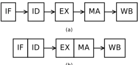
Figure 3: DLX CPU with (a) 5 stages pipeline and (b) 3 stages pipeline. Variable Length Pipelines (also known as Pipeline Stage Unification or Vari-able Stage Pipelines) are useful to improve the throughput. They can be used to reduce leakage with power-gating, as shown in [8, 9]. It limits power con-sumption by reducing the load capacitance of clock drivers, which is achieved by stopping the clock of the bypassed registers; in case of a CPU, it reduces the clock cycle count of program execution by reducing the number of pipeline stages.
2
Implementation
First, we describe intuitively on a simple example how our design works. Then, we detail both implementations and their correctness.
2.1
An Intuitive Example
First, we start with the intuitive example of a simple DLX processor. It is 5-pipeline stages long in Long Pipeline mode, as shown in Figure 3 (a): Instruction fetch cycle (IF), Instruction decode/register fetch (ID), Execution/effective ad-dress cycle (EX), Memory access/branch completion cycle (MEM), Write-back cycle (WB). It has only 3 pipeline stages in Short Pipeline mode : (IF+ID), (EX+MEM) and (WB) as shown in Figure 3 (b).
The basic idea to implement Dynamic Variable Length Pipe-line is to use clock-gating as follows:
• When the pipeline is switching from LP to SP, we need to introduce bub-bles.
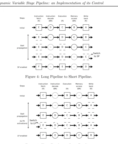
• When the pipeline is switching from SP to LP, we need to remove bubbles. In Figures 4 and 5, plain boxes denotes pipeline stages with regular registers, and dashed boxes denotes stalled stages. Plain circles denotes pipeline stages with bypassable registers; dashed circles denotes bypassed stages.
Switching from LP to SP As shown in Figure 4, we turn off the clock of the first pipeline stage at first instant. At next clock cycle, we will have a bubble in the following BR, that will be switched to its bypassed mode; we also turn off the clock of the third pipeline stage. Then, we will have a bubble in the following BR, and so on. Finally, when reaching the tail of the pipeline, we send to the clock frequency controller a signal to switch to SP, and activate
Dynamic Variable Stage Pipeline: an Implementation of its Control 5
Figure 4: Long Pipeline to Short Pipeline.
Figure 5: Short Pipeline to Long Pipeline.
all stalled stages. The process is safe, since we stall the whole pipeline before switching clock frequency.
Switching from SP to LP As shown in Figure 5, we turn off the clock of the last pipeline stage, and we switch the previous BR in regular register mode, that will receive the new fresh data; at next clock cycle, we turn off the clock of the previous pipeline stage, and switch previous BR in regular register mode, and so on. Finally, when reaching the head of the pipeline, we send to the clock frequency controller a signal to switch to LP, and turn on the clock of all stalled stages.
2.2
Detailed Distributed Implementation
Now we provide mechanism details, implemented using a natural distributed style.
As shown in Figure 6, a local clock-gating stalls the stage upon reception of signal LP toSP or SP toLP , until receiving an enable signal (Done) from
6 Boucaron & Coadou
Figure 6: Distributed implementation.
Clock Generator 0 1 2 1 2 Clock Generator 0 + 2 1 + 1 2 1 + 1 2 (a) (b) (c) (d)
Figure 7: Clock-gating equalization.
the clock generator. When it receives any of such input signal (LP toSP or SP toLP), it simply repeats the signal at the next clock cycle: from a stage to the previous one for SP toLP , and from a stage to both next two stages for LP toSP. When the signal reaches the head (resp. the tail) of the pipeline, then we forward the signal to the clock generator, that will switch from SP to LP (resp. LP to SP). After the clock generator has switched the mode, it enables all stages of the pipeline during the same clock cycle by activation signals (Done). However, activation signals coming from the clock generator to all pipeline stages cannot be achieved within a clock cycle in general, especially in case of very deep pipelines. If turning on/off (through clock-gating) is not performed at the same clock cycle on all stages of the pipeline, there is a correctness issue. The intuitive idea to solve it is to know latencies from/to the clock generator to/from each stage of the pipeline and “equalize” them, with respect to the longest path (latency metric) adding flip-flops (or master/slave latches) when needed. In the example given in Figure 7: the longest paths have a latency of 2 clock cycles in LP mode. We add an additional flip-flop to second and fourth stages, and two flip-flops to third stage. Hence, all stages receive the Done during the same clock cycle.
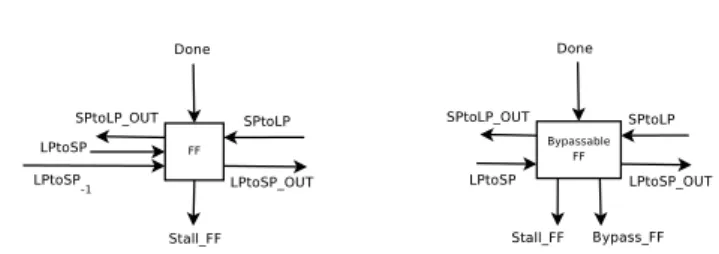
We now detail building blocks used for this implementation (cf. Figure 8). The left one is used in case of regular buffer, while the right one is for bypassable buffers. They both have many common inputs/outputs to implement the distributed protocol. FF has only a StallF F signal to clock-gate its regular
Dynamic Variable Stage Pipeline: an Implementation of its Control 7
Figure 8: Distributed implementation building blocks.
buffer, whereas bypassable FF has an additional signal to drive the mux to bypass.
Each building block has a set of boolean equations that can be easily trans-lated in Verilog, VHDL or SystemC. pre (t) equals the value of signal t during previous clock cycle.
In case of a regular buffer:
LP toSPout = (LP toSP−1∨ LP toSP ∨ pre (LP toSPout))
∧Done
SP toLPout = (SP toLP ∨ pre (SP toLPout)) ∧ Done
StallF F = LP toSPout∨ SP toLPout
where LP toSP−1is the output LP toSPoutfrom the previous FF pipeline buffer,
as shown in Figure 6.
Equations for the bypassable buffer control are as follows: LP toSPout = (LP toSP ∨ pre (LP toSPout)) ∧ Done
SP toLPout = (SP toLP ∨ pre (SP toLPout)) ∧ Done
StallF F = (SP toLP ∨ pre (StallF F)) ∧ ¬LP toSP
∧Done
BypassF F = (LP toSP ∨ pre (BypassF F)) ∧ ¬SP toLP
We assume that Done is not emitted while we are switching pipeline stage modes. This is true by construction, since both pipeline ends, sending LP toSP and SP toLP , are connected to the Clock Generator as shown in Figure 6.
We can put some room in the clock generator to introduce additional buffers, this will not break the current placement and routing; using distributed equal-ization seems better for area, but need to iterate during placement and routing. This equalization introduces mandatory latencies, in order to ensure correct-ness. The longest latency introduces additional cycles of stall in the pipeline when switching from a mode to the other. When switching from SP to LP, we can also use bypassable buffers accordingly to the latency of each path, in order to minimize the number of stalls in the pipeline (it has to be equalized too).
In such distributed implementations, the issue is when we have pipeline configurations that needs to turn off a lot of consecutive stages during the same clock cycle: this cannot be achieved in general, because of long wires. We solve this issue in the next implementation.
8 Boucaron & Coadou
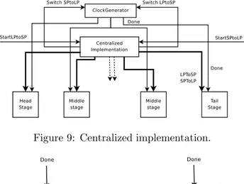
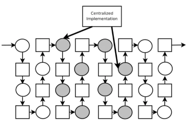
Figure 9: Centralized implementation.
Figure 10: Centralized implementation building blocks.
2.3
Detailed Centralized Implementation
We now discuss a centralized implementation that let us stall any number of pipeline stages during the same clock cycle. The reader should think of central-ized as the root of a clock-tree.
Each pipeline stage has those inputs: LP toSP , SP toLP and Done. They enable the mode switching and the clock, stall the clock, or switch on/off by-passes. Instead of locally generating the stall as in the distributed implemen-tation, now we generate the signal from a module. The module has two inputs associated to mode switching, and has many pair of outputs (LP toSP , SP toLP ) associated to each stage of the pipeline, as shown in Figure 9.
For instance, to switch from LP to SP, as shown in Figure 4, we have to count 10000, 11100, 11111, and finally to send Done to all stages. Another example is to switch from SP to LP as in Figure 5. We just need to count 00001, 00011, 00111, 01111, 11111, and finally to send Done to all stages (assuming here previous latency equalization).
In the centralized implementation, there is no protocol between pipeline stages. We just need a local clock-gating that will receive LP toSP , SP toLP and Done signals. It is no longer needed to equalize latencies from the clock generator to all pipeline stages. In the previous case, the clock generator was not supposed to know how many cycles the pipeline would be fully stalled after it has sent the switch signal. Here, the module can send LP toSP and SP toLP signals with respect to the different latencies of all wires.
Power-gating is an efficient technique to reduce leakage power of a chip. However, power-gating takes more than one clock cycle to be enabled, and also a careful design, as detailed in [3]. The centralized implementation is a good candidate to apply power-gating: when switching from LP to SP, we have the opportunity to turn off a set of flip-flops or latches.
Dynamic Variable Stage Pipeline: an Implementation of its Control 9
Figure 11: Power-gating instance.
Moreover, since both power-gating and switching from LP to SP (and from SP to LP) takes time, we can turn on/off bypassable buffers of pipeline stages, while at the same time we are switching from a pipeline length mode to the other one. This kind of scheme can apply naturally to long pipelines that are regularly found in digital filters for Video, Image and Signal processing, even if all bypassable buffers of such pipeline cannot be turned off because of its length. For instance, let us assume a 32-stages pipeline design, as shown in Figure 11. It takes 8 clock cycles to turn on/off a latch or a flip-flop.
We can neither turn off 8 first stages, nor turn on 8 last stages, because of previous constraints. We can still power-gate 8 stages in between, denoted as grey filled circles in Figure 11. There is an additional time constraint such that power-gate signal arrives on 9th
and 23th
stages within one clock cycle from the centralized scheme; in the first case to turn off, and the second case to turn on respectively. It takes 8 more clock cycles (then a total of 16) if we want to turn on/off all bypassable stages to save more leakage power.
The centralized implementation can be applied to any pipe-line configuration and clock-gating. This cannot be achieved in general using the distributed implementation.
In this implementation, there is only a local clock-gating (or a bypass) on each pipeline stage. There is less area overhead for each stage than in the dis-tributed one (no protocol overhead). However, there are a lot of wires connected from the centralized module to enable/disable clock-gating. More bypassable buffers are also required on each pipeline stage. This means a higher area over-head than with the distributed implementation.
The centralized implementation can cope with any arbitrary latency in the clock-gating scheme, because we can send the enable or stall signals earlier, when building the sequence to switch from one mode to another one.
2.4
Correctness
In order to guarantee the correctness of the switch between the two modes of our design, we have assumed the following hypotheses:
• Only pipelined combinatorial logic can be bypassed. In general, we cannot bypass latches or flip-flops without affecting the behavior. Obviously, if
10 Boucaron & Coadou
the designer knows that it does not change the behaviour, then she/ he can use a bypass.
• There must be at least one latch or flip-flop in any circuit whenever by-passes are active or not. Otherwise, it creates a combinatorial cycle. This is not strictly necessary if shown correct, but most of EDA tools will com-plain in such a case.
• We can clock-gate any pipeline stage within a clock cycle. Otherwise, each pipeline stage could not be seen as a black-box, and a finer grain analysis of latencies and data dependencies would be needed. The centralized implementation can cope with such behaviour.
• Fast clock frequency is a multiple of the slower one. This way, both clocks are phase-aligned; this is a simplification.
• In case of distributed implementation, all the consecutive stages between two bubbles can be stalled within a clock cycle. A problem may occur if a few bubbles are inserted in a long pipeline, far from each other. All stages between two bubbles have to be stalled simultaneously, or there would be misplaced bubbles.
• Clock generator does neither change clock speed, nor send Done when the pipeline is switching from one mode to another.
• Clock tree between pipeline stages and the clock generator is latency equal-ized. Otherwise, there can be issues when the whole pipeline restarts, if the same clock instant does not arrive during the same instant at all pipeline stages.
3
Discussion
In this section, we discuss the timing issues to switch between modes, and hierarchical variable length pipeline.
Time for switching between modes It takes kLP k − kSP k + 1 clock cycles (with the clock frequency of the LP mode) to switch from LP to SP, where kLP k and kSP k are respectively the length of the long and short pipelines. Conversely, it takes the same number of clock cycles to switch from SP to LP, but with the clock frequency of the SP mode. The time for switching between modes is minimal, provided there is no latency from/to clock generator. If there exists such latency, then we have to minimize the latency of the following paths, in order to minimize the time spent for switching between modes:
• From the head of the pipeline, passing through the clock generator, reach-ing all stages of the pipeline.
• From the tail of the pipeline, passing through the clock generator, reaching all stages of the pipeline.
Dynamic Variable Stage Pipeline: an Implementation of its Control 11
Figure 12: Multi-length pipeline.
Hierarchical variable length pipeline Our implementations can also be composed with more than two modes, as shown in Figure 12. The pipeline may have a depth of 5 stages (1 → 2 → 3 → 4 → 5), 3 stages (1 → 2 + 3 → 4 + 5) or 1 stage (1 + 2 + 3 + 4 + 5). A shorter pipeline is obtained by merging consecutive stages of its immediately longer configuration; in other words, there is kind of alignment of the non-bypassed stages from the slowest mode to the fastest. In this case, we come down to the general one, where the times for switching between modes are the same as given above.
4
Conclusion
We introduce two implementations for the control of a Dynamic Variable Length Pipeline through the use of bypassable buffers.
The intuitive idea is as follows: when switching to Long Pipeline (LP) to Short Pipeline (SP), we introduce “bubbles” in bypassable buffers, starting from the head of the pipeline until reaching its tail, then finalizing clock frequency switch; conversely, when switching from Short Pipeline to Long Pipeline, we remove these “bubbles” starting from the tail of the pipeline until reaching its head.
We introduce both distributed and centralized implementation. The dis-tributed implementation simply forwards the switch signal from LP to SP, until reaching the tail, and then re-enables the clock. When switching from SP to LP, we stall the tail of the pipeline, and go in the reverse direction until reaching the head.
All pipeline stages must restart during the same clock-cycle. However, this cannot be done in one clock cycle, when considering long pipelines. To solve this issue in the distributed implementation, we “equalize” latencies of enable paths (from the clock generator to each stage of the pipeline) and also the clock-tree, in between clock generator to stages of the pipeline : we add flip-flops in order to equalize its latency to the longest path, thus synchronizing arrival of all enable signals during the same clock cycle.
Nevertheless, we cannot turn on/off (through clock-gating) a lot of consec-utive stages of the pipeline, because of physical latencies. Hence, we also in-troduce the centralized implementation, allowing more complex configurations that cannot be achieved with the distributed one. There is no need to equalize latencies of enable/stall paths from the clock generator to all pipeline stages in this implementation, but clock-tree equalization is still mandatory to ensure correctness.
12 Boucaron & Coadou
Contents
1 Introduction 3
2 Implementation 4
2.1 An Intuitive Example . . . 4
2.2 Detailed Distributed Implementation . . . 5
2.3 Detailed Centralized Implementation . . . 8
2.4 Correctness . . . 9
3 Discussion 10
4 Conclusion 11
References
[1] Benton H. Calhoun and Anantha P. Chandrakasan. Ultra-dynamic voltage scaling (udvs) using sub-threshold operation and local voltage dithering. IEEE Journal of Solid-State Circuits, 41(1):238–245, January 2006.
[2] B. S. Doyle, S. Datta, M. Doczy, S. Hareland, B. Jin, J. Kavalieros, T. Lin-ton, A. Murthy, R. Rios, and R. Chau. High performance fully-depleted tri-gate cmos transistors. Electron Device Letters, 24(4):263–265, April 2003. [3] Michael Keating, David Flynn, Rob Aitken, Alan Gibbons, and Kaijian Shi. Low Power Methodology Manual: For System-on-Chip Design. Springer-Verlag, 2008.
[4] Changbo Long and Lei He. Distributed sleep transistor network for power reduction. In Proceedings of the 40th Conference on Design Automation (DAC’03), pages 181–186, New York, NY, USA, 2003. ACM.
[5] Siva G. Narendra and Anantha Chandrakasan. Leakage in Nanometer CMOS Technologies. Springer-Verlag New York, Inc., Secaucus, NJ, USA, 2005.
[6] Johan Pouwelse, Koen Langendoen, and Henk Sips. Dynamic voltage scal-ing on a low-power microprocessor. In Proceedscal-ings of the 7th Annual Inter-national Conference on Mobile Computing and Networking (MobiCom’01), pages 251–259, New York, NY, USA, 2001. ACM.
[7] T. Sasaki, Y. Ichikawa, T. Hironaka, T. Kitamura, and T. Kondo. Evaluation of low-energy and high-performance processor using variable stages pipeline technique. Computers and Digital Techniques, IET, 2(3):230–238, May 2008. [8] Hajime Shimada, Hideki Ando, and Toshio Shimada. Pipeline stage unifica-tion: a low-energy consumption technique for future mobile processors. In Proceedings of the 2003 International Symposium on Low Power Electronics and Design (ISLPED’03), pages 326–329, New York, NY, USA, 2003. ACM. [9] Jun Yao, Shinobu Miwa, Hajime Shimada, and Shinji Tomita. Optimal pipeline depth with pipeline stage unification adoption. SIGARCH Com-puter Architecture News, 35(5):3–9, 2007.
Centre de recherche INRIA Sophia Antipolis – Méditerranée 2004, route des Lucioles - BP 93 - 06902 Sophia Antipolis Cedex (France)
Centre de recherche INRIA Bordeaux – Sud Ouest : Domaine Universitaire - 351, cours de la Libération - 33405 Talence Cedex Centre de recherche INRIA Grenoble – Rhône-Alpes : 655, avenue de l’Europe - 38334 Montbonnot Saint-Ismier Centre de recherche INRIA Lille – Nord Europe : Parc Scientifique de la Haute Borne - 40, avenue Halley - 59650 Villeneuve d’Ascq
Centre de recherche INRIA Nancy – Grand Est : LORIA, Technopôle de Nancy-Brabois - Campus scientifique 615, rue du Jardin Botanique - BP 101 - 54602 Villers-lès-Nancy Cedex
Centre de recherche INRIA Paris – Rocquencourt : Domaine de Voluceau - Rocquencourt - BP 105 - 78153 Le Chesnay Cedex Centre de recherche INRIA Rennes – Bretagne Atlantique : IRISA, Campus universitaire de Beaulieu - 35042 Rennes Cedex Centre de recherche INRIA Saclay – Île-de-France : Parc Orsay Université - ZAC des Vignes : 4, rue Jacques Monod - 91893 Orsay Cedex
Éditeur
INRIA - Domaine de Voluceau - Rocquencourt, BP 105 - 78153 Le Chesnay Cedex (France)
http://www.inria.fr