HAL Id: tel-02373919
https://tel.archives-ouvertes.fr/tel-02373919
Submitted on 21 Nov 2019HAL is a multi-disciplinary open access archive for the deposit and dissemination of sci-entific research documents, whether they are pub-lished or not. The documents may come from teaching and research institutions in France or
L’archive ouverte pluridisciplinaire HAL, est destinée au dépôt et à la diffusion de documents scientifiques de niveau recherche, publiés ou non, émanant des établissements d’enseignement et de recherche français ou étrangers, des laboratoires
Engineering of magnetic tunnel junction stacks for
improved STT-MRAM performance and development of
novel and cost-effective nano-patterning techniques
Jyotirmoy Chatterjee
To cite this version:
Jyotirmoy Chatterjee. Engineering of magnetic tunnel junction stacks for improved STT-MRAM performance and development of novel and cost-effective nano-patterning techniques. Micro and nan-otechnologies/Microelectronics. Université Grenoble Alpes, 2018. English. �NNT : 2018GREAT130�. �tel-02373919�
DOCTEUR DE LA
COMMUNAUTÉ UNIVERSITÉ GRENOBLE ALPES
Spécialité : NANO ELECTRONIQUE ET NANO TECHNOLOGIES Arrêté ministériel : 25 mai 2016Présentée par
Jyotirmoy CHATTERJEE
Thèse dirigée par Bernard DIENY , CEA et codirigée par Olivier JOUBERT, CNRS
préparée au sein du Laboratoire Spintronique et Technologie des Composants
dans l'École Doctorale Electronique, Electrotechnique, Automatique, Traitement du Signal (EEATS)
optimisation de jonctions tunnel
magnétiques pour STT-MRAM et
développement d'un nouveau procédé de
nanostructuration de ces jonctions.
Engineering of magnetic tunnel junction
stacks for improved STT-MRAM performance
and development of novel and cost-effective
nano-patterning techniques.
Thèse soutenue publiquement le 29 mars 2018, devant le jury composé de :
Monsieur Bernard DIENY
Directeur de Recherche, Spintec, Directeur de thèse Monsieur Stéphane MANGIN
Professeur, Université de Lorraine, Rapporteur Monsieur Dafine RAVELOSONA
Directeur de Recherche, CNRS, Rapporteur Monsieur Jan VOGEL
Directeur de Recherche, CNRS, Examinateur Monsieur Jean-Marie GEORGE
Directeur de Recherche, CNRS, Examinateur Monsieur Ahmad BSIESY
This PhD work is successful and important achievement of my academic career. However, behind this success there are many people who supported me mentally, physically and intellectually. I would like to take this opportunity for expressing my gratitude to all of them.
For me it is not merely 3 or 4 years of journey, rather I believe that it started when I had first learnt a letter and number from my mother. At first, I would like to thank my parents for constantly supporting me from the beginning. I must emphasize that, without the effort and guidance of my father and especially my mother during my childhood it would not have been possible to continue this journey.
I am very thankful to my wife for always being present beside me, supporting me during my stressful time, taking care about the important works for which I could not make time, and most importantly for always loving me.
I don’t know how to thank my PhD supervisor, Bernard Dieny. There was a time, I almost lost hope to continue my research career. In that critical situation, Bernard gave me a chance offering me a PhD position under his supervision. I would like to express my deepest gratitude for giving me the opportunity not only to restart my research career but most importantly evaluating myself. I started my PhD at Spintec in December 2014. From that time, I have interacted with him many times. I must admit that, most of the time I just knocked the door and entered inside. I am thankful that Bernard made himself almost always available for discussion.
A suggestion for the present students: never hesitate to knock his door if you have some question or have some ideas to discuss. If you do so, you are going to save lot of time and you will work effectively. But I must warn you about one thing. Suppose, Bernard suggests to execute some experiments or measurements, which you don’t think very important and skip. Later, when you realize that you are wrong, then you should know that he will remember about the discussion. He will remember the suggestion that he gave you before. So, when you meet him after, don’t say that you did not do it. Rather you say that you are doing it. But don’t worry, even if you say that you did not do it. In this three years time, I have never seen him angry or displeased. I never heard any unenthusiastic words from him. He has always encouraged and appreciated me. I feel myself very lucky
knowledge and always supported me. Bernard also has indirectly taught me how to work efficiently remaining cool. I am still working on it. My deepest thanks and gratitude for everything you did for me.
With my past experience, I must emphasize that, apart from knowledge and resources it is equally important for a PhD student, to get work-freedom and friendly atmosphere for research. This helps a student to stay focused on their scientific topic developing new ideas or analyzing and understanding certain phenomena. I must tell the present students of Spintec that, not all groups or institutes have such kind of friendly atmosphere. Even you may not get enough research freedom. Therefore, you are lucky to work in Spintec. Hence, I would like to thank, previous director Jean-Pierre Nozieres, current director
Lucian Prejbeanu, all the administrative members, permanent scientific and
non-scientific staffs of Spintec for maintaining a friendly research environment in our lab. I would like to thank Lucian once again for helping me preparing many presentations and other important technical and non-technical suggestions.
A big thank to Ricardo Sousa for the scientific discussion and all of his advices during first one and half year of my PhD. Ricardo taught me many things. I would have learnt more, especially about the electrical characterization if I could have got him for the rest of the PhD period.
I would like to thank my co-supervisor Olivier Joubert for the MINOS grant and for the advice on nano-patterning, and support for my job search.
A big thank to Stephane Auffret. He taught me the deposition tool repeatedly explaining some commands written in French. I must admit that, whenever I asked any samples, he deposited as quickly as possible. Even sometime, I stopped him launching the deposition and asked to include some stacks and he did it with a smile.
I would like to thank and appreciate Laurent Vila for all the e-beam lithography and his suggestion and discussion about fabrication. He is such a nice and friendly person. I would regret that I could not work with him directly. For device fabrication, I would like to acknowledge also Jude, Nathalie and Yoann.
I appreciate and acknowledge Clarisse Ducruet for the CIPT measurements.
During my PhD, I had opportunity to collaboratively work with many people. First, I would like to thank Eric Gautier for teaching me sample preparation using FIB and also for the help for HRTEM imaging. I also would like to thank Stephane Lequien for teaching me XRD and XRR measurement. We have very good collaboration with Marc
I worked also in collaboration with Farid Fettar and Jean-Marc Tonnerre. I am grateful to Farid for allowing me to use SQUID and other characterization tools in Neel institute. I would like to thank Jean-Marc to carry out XMCD measurement. Although I could not include everything in my thesis but I hope, soon we will be able to publish. I would like to thank Thomas Serbeak for the polarized neutron reflectometry measurement. It has been a wonderful experience working with all of you.
I will miss our coolest Spintec office. I will miss the flavor of the blend of
Paulo-Mathieu-Jyotirmoy-Titiksha. It was coolest and funny because we got Paulo ingredient in
our office. I had spent great time with you guys discussing and understanding many topics including our research topics. Special thanks to Paulo and Mathieu for explaining many letters time to time, and your help to finish some official work as well.
I would like to thank other MRAM group members: Lea, Tan, Andrey, Nikita, Van Dai,
Nicolas, Luc, Antoine, Miguel for many useful discussions, collaborative work and some
jokes in the lab. I would like to thank Gills, Alex, Alexu, Jeremi, Safeer, Lamprini,
Chandra, Jay, Debapriyo, Daniel, Youssouf, Romeo and all the other Spintec’s PhD and
postdocs for the wonderful time I have spent with all of you.
A special thank to Youssouf, Gill Gaudin and Olivier Boulle for their support on the work on SOT-MRAM.
I would like to thank some friends from Belgium, Gouri Shankar, Mitali, Urmimala
Swaraj, Swarup and Sonai for always being beside my family and me. Your words
helped us to get through a tough period in 2014. I would like to acknowledge some of my teachers from India for their helpful guidance and knowledge.
Here in Grenoble, I would like to thank the families of Chandra-Swarnalatha, Priyadarshini-Ananda and Mitesh-Bhabisha for the wonderful moment we spent together. My little daughter Rupu, perhaps now she will not understand, that the moments I spent with her were very precious. It helped me to forget negative thoughts and enjoy the moment with her. She drags me from the past or from the future forcing me to live in present, which saves my positive energy.
At the end, I would like to thank all the people who helped me and my family to live in Grenoble happily and peacefully accomplishing our work.
1 BACKGROUND AND CONTEXT 7
1.1 GMR 10
1.2 TMR 11
1.2.1 Jullière Model 11
1.2.2 Slonczewski Model 14
1.2.3 Spin filtering effect by coherent tunneling 16 1.2.4 CIPT technique for TMR and RA measurements 17
1.3 SPIN-TRANSFER TORQUE 19
1.3.1 Spin-transfer torque and magnetization dynamics 20
1.4 INTRODUCTION TO STT-MRAM 22
1.4.1 Different families of MRAM 22 1.4.2 In-plane vs. perpendicular STT-MRAM 24 1.4.3 Properties of material for designing STT-MRAM 25
1.5 PERPENDICULAR MAGNETIC ANISOTROPY : ORIGIN & APPLICATIONS 28
1.5.1 PMA due to magnetocrystalline anisotropy 30 1.5.2 Interfacial origin of PMA 31 1.5.3 Experimental determination of interfacial and volume anisotropy energies 33
1.6 CONCLUSIONS 35
1.7 BIBLIOGRAPHY 36
2 STRUCTURAL, MAGNETIC AND TRANSPORT PROPERTIES OF
PERPENDICULAR MAGNETIC TUNNEL JUNCTION STACKS WITH
REFRACTORY METALS IN THE CAP 41
2.1 IMPROVEMENT OF STORAGE ELECTRODE’S ANNEALING TOLERANCE 44
2.1.1 Significance of post-deposition annealing of MTJ stack 44 2.1.2 Highest annealing tolerance of top storage electrode 45 2.1.3 Origin of enhanced annealing tolerance 48
2.2 ANNEALING TEMPERATURE DEPENDENCE OF MAGNETIC PROPERTIES OF
STORAGE ELECTRODE WITH Ta 1 AND W2/Ta1 nm CAP 49
2.2.1 Magnetic properties by MOKE mapping and determination of transition thickness and magnetic
dead layer thickness 50
2.2.2 Anisotropy constant, saturation magnetization, dead layer thickness of FeCoB with W/Ta and Ta
cap 53
2.2.3 Why PMA of FeCoB with W cap is higher than with Ta? 55
2.3 MAGNETIC AND TRANSPORT PROPERTIES OF pMTJ FILMS AND PATTERNED
DEVICES 56
2.3.1 pMTJ films at various annealing stages 56 2.3.2 TMR of patterned memory devices and correlation with structural properties 58 2.3.3 Thermal stability factor (Δ) of patterned memory devices 61
2.4 CONCLUSIONS 64
3 NOVEL RKKY COUPLING LAYER: A ROUTE TOWARDS EXTREMELY
THIN PMTJ STACKS 67
3.1 SIGNIFICANCE OF SYNTHETIC ANTIFERROMAGNETIC LAYERS IN SPINTRONIC
DEVICES 70
3.2 STATE OF THE ART 72
3.3 MAGNETIC PROPERTIES OF pSAF AND pMTJ USING Ru/W RKKY COUPLING LAYER
75
3.3.1 RKKY coupling energy versus Ru/W thicknesses 75 3.3.2 Magnetic properties of thin-pMTJ stacks with annealing 77 3.3.3 How to control the concurrent reversal of thin-pSAF ? 79
3.4 ELECTRICAL PROPERTIES OF THIN-pMTJ 84
3.5 CONCLUSIONS 86
3.6 BIBLIOGRAPHY 87
4 COMPOSITE STORAGE LAYERS WITH DIFFERENT MAGNETIC AND
NON-MAGNETIC INSERTION 89
4.1 COMPOSITE STORAGE LAYER: Ta VERSUS W SPACER 92
4.1.1 Magnetic properties with different annealing temperature 92 4.1.2 Magnetic properties as function of W spacer thickness 95 4.1.3 Optimization of the position of the W spacer within the FeCoB CSL 97
4.2 COMPOSITE STORAGE LAYER: DIFFERENT MAGNETIC INSERTIONS 99
4.3 COMPOSITE STORAGE WITH DUAL W LAMINATIONS 101
4.3.1 Magnetic and transport properties at room temperature 102 4.3.2 Magnetic properties as a function of temperature 104
4.4 CONCLUSIONS 109
4.5 BIBLIOGRAPHY 110
5 SEEDLESS MULTILAYER WITH PMA AND ADVANCED STACKS FOR
MEMORY APPLICATIONS 111
5.1 SEEDLESS MULTILAYERS WITH PMA 114
5.1.1 Co/Pt multilayers with Pt thickness variation 115 5.1.2 Influence of non-magnetic layer insertion between Co and Pt 116 5.1.3 Variation of texture breaking layer’s thickness 118 5.1.4 Thickness variation of Pt, Ta and Co in [Co/Ta/Pt] multilayers 120
5.2 ADVANCED SPINTRONIC DEVICE STACKS 123
5.2.1 Top-pinned pMTJ stacks for STT-MRAM 123 5.2.2 Double magnetic tunnel junctions 125 5.2.1.1 Towards thin-DMTJs 128 5.2.3 Top-pinned pMTJ stacks for SOT-MRAM applications 131
5.2.4 Multibit memory 135
5.4 ACKNOWLEDGEMENT 139
5.5 BIBLIOGRAPHY 140
6 NOVEL NANOPATTERNING TECHNIQUES FOR STT-MRAM
FABRICATION 143
6.1 MOTIVATION 146
6.2 METHOD-1: PRE-PATTERNED NANO-PILLARS 148
6.2.1 Description of fabrication process 148 6.2.2 First experiments with W nano-pillars prepared by damascene approach 149 6.2.3 Experiments with Ta nano-pillars fabricated by RIE 151 6.3.1.1 Fabrication of Ta nanopillars 152 6.3.1.2 Structural properties of patterned cells 154 6.3.1.3 Magnetic and Transport properties of patterned cells 155
6.3 METHOD-2: PRE-PATTERNED NANO-HOLES 157
6.3.1 Nano-holes with bilayers e-beam resist 158 6.3.2 Nano-holes with four-layers e-beam resist 160
6.4 CONCLUSIONS 163
6.5 BIBLIOGRAPHY 164
GENERAL INTRODUCTION
Science and technology for mankind in twenty first century is not imaginable without the data storage technology. Transmission and storing information play major role in current computing technology. Magnetism introduced the very first wire recording technology in 1898, which was invented by Valdemar Poulsen. The recording technology was revolutionized with the advent of magnetic tapes recording in 1928. Magnetic oxide (Iron oxide) coated on a flexible substrate was used for storing the information. Hard disk drive (HDD) invented by IBM was first used in computers (IBM 305 RAMAC) in 1956 with read/write operation. In contrast to tape recorders, HDD use solid disks, coated with magnetic material, and paired with a read/write head. The areal density at that time was limited to 2000 bits/inch2. Moreover, the first nonvolatile magnetic random access memory (MRAM) was designed by J. W. Forrester in 1950 using small ferrite rings. However, after the invention of the transistor, one-transistor-one-capacitor based volatile dynamic-RAM (DRAM) cell was designed in 1970s, which obsoleted the nonvolatile magnetic core memory due to the advantages of scalability, cost-effectiveness and speed. The discovery of giant magnetoresistance (GMR) in 1988 by P. Gruenberg [1] and A. Fert [2] was a major breakthrough. A new field of research and development named Spintronics emerged from this discovery, employing “spin” degree of freedom of electrons along with the charge. The development of spintronics since the early 90’s is paved with a number of breakthrough discoveries such as tunneling magnetoresistance (TMR) [3] and spin transfer torque (STT) [4], [5]. These key achievements of GMR and giant TMR [6]–[8] in Spintronics research field revolutionized HDD industry, allowing a tremendously increase in the storage areal density (1.3 Tbits/inch2 in 2015). The discovery of spin-transfer torque STT opened the avenue for the manipulation of the magnetization of magnetic nanostructures by spin-polarized electrical current rather than by magnetic field. Spintronics community reenergised from the demonstration of STT. One of the key memory device proposed based on STT phenomenon is spin-transfer torque magnetic random access memory (STT-MRAM). Nowadays, most of the attention is focused on out-of-plane magnetized STT-MRAM based on perpendicular magnetic tunnel junction (pMTJ).
General introduction
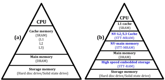
Figure I.1: (a) Current memory hierarchy and (b) future low power memory hierarchy combining STT-MRAM with CMOS technology.
They gather many advantageous characteristics namely non-volatility, quasi-infinite endurance, high retention, low energy consumption, scalability down to sub-20nm technology nodes, high speed (~ns) and CMOS compatibility.These properties make STT-MRAM along with its other variants such as spin orbit torque MRAM (SOT-MRAM) and domain wall motion MRAM, an ideal candidate for a universal memory.
Nowadays, to speed up the transfer of information between where the data are stored (Hard disk drive or Solid State Drive) to where they are processed, various levels of memories are used and organized along a certain hierarchy (Figure I.1). It comprises the fast (~ns) and low density cache memory made of SRAM close to the logic blocks, the main memory (DRAM) of high density (several Gbit) and moderately high speed (30 to 100ns) and storage (slow access time ~ms but very high density ~several Tbit). Among those, the cache memory (static random access memory (SRAM)) and main memory (DRAM) are volatile meaning that they must be constantly power supplied to keep the information. There are speed gaps between cache memory and main memory as well as between main memory and storage. With the shrinking of technology node, the speed gaps become wider as well as energy consumption in standby mode increases due to increasing leakage in the CMOS transistors at the most advanced technology nodes. As a matter of fact, in current microprocessors, the leakage power consumption is almost as large as the dynamic power consumption. To solve these problems and in first place the issue of power consumption, STT-MRAM can be introduced in the memory hierarchy to
Main memory (DRAM) Cache memory (SRAM) (L1 L2 L3) CPU Storage memory (Hard disc drive/Solid state drive) (a) Main memory (DRAM) L1 cache (SRAM) CPU NV-L2/L3 Cache (STT-MRAM) Storage memory (Hard disc drive/Solid state drive) High speed embedded storage (STT-RAM) NV-main memory (STT-MRAM) (b)
reduce the leakage power consumption by taking advantage of the non-volatility of these memory and for increasing the bandwidth between memory and logic by bringing the memory closer to the logic blocks with a much finer granularity then in current architectures. Thus, STT-MRAM as NV-Cache and NV-main memory, thanks to their non-volatility, reduces power consumption by cutting off the power supply of all blocks, which are temporarily inactive. The concept of Normally-off/Instant-on electronics was introduced to describe this new type of architectures. The near future memory architecture embedding STT-MRAM is illustrated in Figure I.1 (b). In far future, complete non-volatile architecture as shown in figure I.2 is envisaged in order to completely eliminate the standby power consumption as well as to speed up transmission of data between storage and logic.
Figure I.2: Memory hierarchy with non-volatile main memory and non-volatile logic blocks architecture for ultra-low power computing.
Employing STT-MRAM with other alternative MRAM such as SOT-MRAM and domain wall motion MRAM in the memory hierarchy demands material development and optimization to solve the existing challenges. The objectives of my thesis are to solve (a) some of the material challenges by engineering the different parts of pMTJ stacks to improve their magneto-transport property and (b) integration challenge of high density and high capacity memory array demonstrating novel nano-patterning techniques.
The important results of these three years’ research work will be organized into six chapters in this thesis.
NV-Main memory NV-Logic with memory Storage memory (Hard disc drive/Solid state drive)
General introduction
Chapter-1 describes the important fundamental spintronic phenomena, which are relevant to the context of this thesis along with historical background and literature review. A brief introduction about STT-MRAM is given, illustrating material requirements for high performance STT-MRAM, different generations of MRAM, comparing in-plane and perpendicular easy axis STT-MRAM as well as the origin of perpendicular magnetic anisotropy (PMA).
Chaper-2 is dedicated to discuss the beneficial influence of introducing a refractory metal (W) in the cap of FeCoB storage layer. A detailed comparative study of annealing temperature dependent magnetic, structural and transport properties of pMTJ stacks as well as patterned memory cells with Ta and W/Ta cap layers is presented. This study demonstrates a record annealing stability of storage electrode with thicker W in W/Ta cap. These observations are supported by detailed physicochemical investigations of these stacks. Besides, a significant improvement of PMA of FeCoB storage electrode using W/Ta cap in compared with Ta cap is demonstrated. This yields a significant enhancement in thermal stability factor and TMR of patterned memory cell.
Chapter-3 explains the development and optimization of a novel multifunctional RKKY layer and its importance to extremely reduce the thickness of pMTJ stacks, which is beneficial for the fabrication and particularly the etching of STT-MRAM cells. The magnetic properties of thin perpendicular synthetic antiferromagnetic layer (thin-pSAFs) as well as thin-pMTJs are systematically studied. The electrical characterizations of patterned memory cells made from the thin-pMTJ stacks demonstrate adequate stability of the reference layer against applied voltage pulse enabling its use for reliable STT-MRAM application.
Chapter-4 extends the study of enhancing the PMA of storage layer as demonstrated in chapter-2 by investigating the magnetic properties of various composite storage layers (CSLs) as a function of annealing temperature. In the course of this work, the role of Ta and W spacer layers and of different magnetic insertion (Co60Fe20B20, NiFe etc) on the magnetic property of CSLs was studied as a function of annealing temperature. The prime motivation was to develop a CSL with higher Curie temperature for high temperature application (mostly automotive and industrial applications). In this context, a novel design of dual-W-CSLs sandwiching different magnetic materials (Fe72Co8B20, Co60Fe20B20 and Co) between two W laminations was proposed and the magnetic
Chapter-5 presents the development of a novel seedless multilayers (MLs) resulting in higher PMA than the conventional Co/Pt MLs. The best seedless MLs are realized by inserting a thin Ta layer between Co and Pt, which is subsequently optimized by varying the thicknesses of each component. The second counterpart of this chapter reveals different types of memory architectures using (Co/Ta/Pt) seedless MLs such as, (i) double barrier pMTJ stacks for STT-MRAM applications, (ii) a top-pinned pMTJ stacks for SOT-MRAM applications and (iii) a novel stack for two bits memory cell with independent one-step spin-orbit-torque induced writing of two storage layers. These stacks are promising for low power consumption, high speed and relatively denser memory applications
Chapter-6 shades light on integration of high density, high capacity memory array, which is promising for DRAM replacement by STT-MRAM. Two unconventional nano-patterning techniques, one using deposition of MTJ stacks on pre-patterned non-magnetic metallic nano-pillars and the other in pre-patterned nano-holes are discussed. The first part starts with the technological development of conducting nano-pillars fabrication with undercut. The magnetic, structural and electrical properties of memory cells obtained by depositing pMTJ stacks on these patterned pillars are illustrated in details. A record density of 1.5F pitch size (F=MTJ diameter) with functional STT-MRAM cells are demonstrated using this technique. The second part presents the nano-hole fabrication and patterning of memory cell by depositing a simple MTJ stack in the nano-holes by sputtering and e-beam evaporation techniques.
BIBLIOGRAPHY
[1] G. Binasch, P. Grünberg, F. Saurenbach, and W. Zinn, “Enhanced
magnetoresistance in layered magnetic structures with antiferromagnetic interlayer exchange,” Phys. Rev. B, vol. 39, no. 7, pp. 4828–4830, 1989.
[2] M. N. Baibich, J. M. Broto, A. Fert, F. N. Van Dau, F. Petroff, P. Eitenne, G. Creuzet, A. Friederich, and J. Chazelas, “Giant magnetoresistance of
(001)Fe/(001)Cr magnetic superlattices,” Phys. Rev. Lett., vol. 61, no. 21, pp. 2472–2475, 1988.
[3] M. Julliere, “TUNNELING BETWEEN FERROMAGNETIC FILMS,” Phys Lett, vol. 54, no. 3, pp. 225–226, 1975.
[4] J. C. Slonczewski, “Current-driven excitation of magnetic multilayers,” J. Magn.
Magn. Mater., vol. 159, no. 1–2, pp. L1–L7, Jun. 1996.
[5] L. Berger, “Emission of spin waves by a magnetic multilayer traversed by a current L.,” Phys. Rev. B, vol. 54, no. 13, pp. 9353–9358, 1996.
General introduction
tunneling conductance of Fe|MgO|Fe sandwiches,” Phys. Rev. B, vol. 63, no. 5, pp. 1–12, Jan. 2001.
[7] S. Yuasa, T. Nagahama, A. Fukushima, Y. Suzuki, and K. Ando, “Giant room-temperature magnetoresistance in single-crystal Fe/MgO/Fe magnetic tunnel junctions,” Nat. Mater., vol. 3, no. 12, pp. 868–871, 2004.
[8] S. S. P. Parkin, C. Kaiser, A. Panchula, P. M. Rice, B. Hughes, M. Samant, and S.-H. Yang, “Giant tunnelling magnetoresistance at room temperature with MgO (100) tunnel barriers.,” Nat. Mater., vol. 3, no. 12, pp. 862–7, Dec. 2004.
CHAPTER: I
1 Background and Context
Table of Contents
1.1 GMR 10
1.2 TMR 11
1.2.1 Jullière Model 11
1.2.2 Slonczewski Model 14
1.2.3 Spin filtering effect by coherent tunneling 16 1.2.4 CIPT technique for TMR and RA measurements 17
1.3 SPIN-TRANSFER TORQUE 19
1.3.1 Spin-transfer torque and magnetization dynamics 20
1.4 INTRODUCTION TO STT-MRAM 22
1.4.1 Different families of MRAM 22 1.4.2 In-plane vs. perpendicular STT-MRAM 24 1.4.3 Properties of material for designing STT-MRAM 25
1.5 PERPENDICULAR MAGNETIC ANISOTROPY : ORIGIN &
APPLICATIONS 28
1.5.1 PMA due to magnetocrystalline anisotropy 30 1.5.2 Interfacial origin of PMA 31 1.5.3 Experimental determination of interfacial and volume anisotropy energies 33
1.6 CONCLUSIONS 35
1.7 BIBLIOGRAPHY 36
Spintronics is integration of magnetism and electronics combining both charge (e) and spin angular momentum ( ħ/2) degrees of freedom of electrons. At present, numerous spintronic devices have been conceptualized and also practically realized by combining two spintronic mechanisms. The first one associated with the manipulation of the charge current via the magnetic configuration of the system by taking advantage of spin-dependent transport properties. This mechanism encompasses magnetoresistive phenomena such as giant magnetoresistance (GMR) or tunneling magnetoresistance (TMR). The second mechanism is the possibility to modify magnetic configuration thanks to a spin-polarized current via angular momentum transfer. Examples of this mechanism are spin-transfer torques (STT) and spin-orbit torques (SOT). By combining the above-mentioned spintronic effects, numerous devices such as magnetic random access memory (MRAM), magnetoresistive sensors, oscillators and spin-logic devices etc. have been invented.
As my thesis is on perpendicularly magnetized-STT-MRAM (pSTT-MRAM), I will briefly introduce the related phenomena: TMR and STT. A brief description will be included regarding how MRAM evolved from first generation to present configuration. Subsequently, I will discuss the important properties and optimal design of material stack that are required to obtain desired device performances. An explanation about the origin of perpendicular magnetic anisotropy (PMA) and its significance for STT-MRAM will also be given. The experimental techniques used for this research will also be included in the related part of discussion.
The discovery of giant magnetoresistance (GMR) in 1988 by A. Fert and P. Grünberg was a major breakthrough [1],[2] and boosted up the research work in Spintronics. In 2007, they were awarded Nobel prize in Physics for recognition of the impact of this discovery in science and technology. In terms of practical application, this phenomenon was tremendously important for hard disk drive (HDD) industry. Indeed, soon after the discovery of GMR, low field GMR sensors called spin-valves, suitable for hard disk drives read heads, were invented 1991[3]. IBM introduced them in the read heads in 1998, which was the first GMR based product. Tunnel magnetoresistance was discovered more than a decade before GMR observation, by Jullière in 1975, using a Fe/GeOx/Co tunnel junction [4]. However the TMR values obtained was 14% at 4.2K. Two decades later, room temperature TMR of 11.8% was demonstrated by Moodera in 1995 by using
1.1 GMR
TMR in Fe/MgO/Fe MTJ [6]. He predicted symmetry based spin filtering effect and 1000% TMR for this tri-layer system. Soon after, in 2004, Yuasa and Parkin experimentally demonstrated giant TMR (200%) using crystalline MTJ of Fe/MgO/Fe and CoFe/MgO/CoFe [7], [8]. These key achievements in Spintronics research field revolutionized HDD industry and accelerated the development of magnetic random access memory (MRAM) technology.
1.1 GMR
The GMR ratio is defined as (RAP-RP)/RP, where RAP and RP are the resistances of “ferromagnet/metal/ferromagnet or ferromagnet/insulator/ferromagnet” trilayers when the magnetizations are in anti-parallel and parallel orientation respectively. The theory of GMR is different from TMR. In case of GMR, the spin dependent scattering of electrons yields different resistances for parallel and anti-parallel magnetization orientations, which is explained by Mott’s two current model [9]. According to this model, in the low temperature limit, one can consider that conduction of spin up (↑) and spin down (↓) electrons take place in two independent parallel channels. Figure 1.1 shows current-perpendicular-to-plane (CPP) geometry of ferromagnetic metal (Co)/Normal metal (Cu)/Ferromagnetic metal (Co) multilayers for GMR. For Co, majority electron, spin up (↑) has low density of states at Fermi energy compared to minority, spin down (↓) electrons. Actually, the Fermi energy (EF) lies above the 3d↑ sub band. It is well known from the Fermi Golden rule, that the scattering probability of electrons is proportional to the density of states. When magnetizations of both the Co layers are in parallel alignment, the minority electrons undergo more scattering compared to majority electrons while travelling across the multilayers under an applied bias. If we denote the resistance of the ferromagnetic layer for majority electrons as r and minority electrons as R, then r<R and the total resistance for parallel alignment is RP=2Rr/(R+r). In case of anti-parallel alignment, spin up (↑) electrons become minority and spin downs (↓) become majority in the second Co electrode. Therefore, spin up (↑) electrons are weakly scattered as majority electrons in the first Co layer but strongly scattered as minority electrons in the second Co layer. Similarly, spin down (↓) electrons are strongly scattered as minority electrons in the first Co layer but weakly scattered as majority electrons in the second Co layer. Hence the total resistance becomes, RAP= (R+r)/2. Note that, in the calculation of total resistance, the resistance of Cu layer has been neglected for simplification.
Figure 1.1: Illustration of GMR using two current model. This explains the conduction of spin-up and spin-down electron in Co/Cu/Co multilayer for CPP geometry.
Then GMR can be simply expressed as:
𝐺𝑀𝑅 =𝑅!"𝑅− 𝑅! ! =(𝑅 − 𝑟)
!
4𝑅𝑟 (1.1)
1.2 TMR
Tunneling magnetoresistance ratio (TMR) ratio is a parameter to measure transport property of magnetic tunnel junctions (MTJs) with ferromagnet /insulator /ferromagnet trilayers. This configuration is similar to CPP-GMR geometry- only the non-magnetic layer is replaced by an insulating oxide barrier. Therefore, the transport mechanism across MTJ is ballistic governed by quantum mechanical tunneling effect across the potential barrier created by the oxide layer. However, at first, a simple model was proposed by Jullière to explain the TMR effect [4].
1.2.1 Jullière Model
This model has been illustrated in Figure 1.2. Under an applied bias, there is a net electron tunneling current from ferromagnetic-1 electrode to 2. This tunneling current is
𝑅! = 2𝑅𝑟 (𝑅 + 𝑟) 𝑅!" =𝑅 + 𝑟 2
Co
Cu
Co
Co
Cu
Co
r
r
R
R
r
r
R
R
1.2 TMR
unoccupied states in ferromagnet-2. Under low temperature limit and low applied bias, this current is proportional to the product of density of states at Fermi energy [D1(EF)*D2(EF)]. When magnetization orientations of both ferromagnetic electrodes are
parallel, the majority electrons (spin-up, ↑, parallel to magnetization direction) from ferromagnet-1 tunnels to the unoccupied majority spin states at Fermi level of ferromagnet-2.
Figure 1.2: Illustration of GMR using two current model. This explains the conduction of spin-up and spin-down electron in Co/Cu/Co multilayer for CPP geometry.
Similarly, the minority electrons (spin-down, ↓, antiparallel to magnetization direction) from ferromagnet-1 also tunnel to the unoccupied minority states at Fermi energy of ferromagnet-2. Therefore, the conductance (GP) in case of parallel magnetization
orientation can be written as
𝐺! ∝ 𝐷!↑(𝐸!)𝐷!↑(𝐸!) + 𝐷!↓(𝐸!)𝐷!↓(𝐸!) (1.2)
In case of antiparallel magnetization orientation of the electrodes, the majority and minority electrons from ferromagnet-1 tunnel to the unoccupied minority and majority states at Fermi energy of ferromagnet-1 respectively. Therefore, the conductance (GAP) in
case of antiparallel magnetization orientation can be written as.
𝐺!"∝ 𝐷!↑(𝐸!)𝐷!↓(𝐸!) + 𝐷!↓(𝐸!)𝐷!↑(𝐸!) (1.3)
Let’s define a parameter ai as a fraction of majority electrons in the i-th electrode, where i
being 1 or 2 electrode. Then, ai can be written as,
𝑎! =
𝑛!↑ 𝐸!
𝑛!↑ 𝐸! + 𝑛!↓(𝐸!) =
𝐷!↑ 𝐸!
𝐷!↑ 𝐸! + 𝐷!↓(𝐸!) (1.4)
Therefore, the spin polarization of ferromagnetic electrodes P1 and P2 are expressed by,
𝑃! = 𝐷!↑ 𝐸! − 𝐷!↓(𝐸!) 𝐷!↑ 𝐸! + 𝐷!↓(𝐸!) = 2𝑎!− 1 (1.5) 𝑃! =𝐷!↑ 𝐸! − 𝐷!↓(𝐸!) 𝐷!↑ 𝐸! + 𝐷!↓(𝐸!) = 2𝑎!− 1 (1.6)
Using the equation 1.4 the conductance in parallel (GP) and antiparallel (GAP) alignment
can be written as
𝐺! ∝ 𝑎!𝑎!+ (1 − 𝑎!)(1 − 𝑎!) (1.7)
𝐺!" ∝ 𝑎!(1 − 𝑎!) + (1 − 𝑎!)𝑎! (1.8)
Using the equations 1.5 to 1.8, TMR can be written as
𝑇𝑀𝑅 = 𝐺!𝐺− 𝐺!"!" = 𝑅!"𝑅− 𝑅! ! = 1 − 𝑃2𝑃!𝑃!!𝑃! (1.9)
Jullière model accurately predicted TMR values of MTJs consisting of Co, Ni and CoFe alloy with amorphous Aluminum oxide barrier. However, this model could not predict the sign of spin polarization for Co and Ni. The giant TMR values obtained for MTJ with MgO crystalline tunnel barrier could not either be explained by this model. This model
1.2 TMR
a
0
eV
E
FE
Fϕ
only considers the properties of the ferromagnetic electrodes were considered through the expression of spin polarization. The insulating barrier itself does not play a role in the calculation of the tunneling magnetoresistance in Julliere’s model.
1.2.2 Slonczewski Model
Slonczewski performed a detailed quantum mechanical calculation to calculate the tunneling conductance of magnetic tunnel junctions as a function of relative angle between magnetizations (θ) of two ferromagnetic metals [10]. He assumed the free electron of the two identical magnetic metals participate for tunneling across the insulator. This insulator is considered as a rectangular potential barrier with height of φ and width of a. Basically, the free electron with energy E propagates as a plane waves with wave vector k to the barrier. The electron wave function decays exponentially with a decay coefficient 𝜅 = 2𝑚!(𝜙 − 𝐸)/ℏ! in the tunnel barrier. Finally, the transmitted
electron propagates again as a plane wave in the second ferromagnetic metals. Solving the Schrodinger equation, the transmission probability of electrons with particular spin states can be written as,
𝑇!! ! = 16𝜅!𝑘!𝑘!!𝑒!!!" 𝑘!!+ 𝜅! 𝑘 !!!+ 𝜅! (1.10)
Figure 1.3: Illustration of GMR using two current model. This explains the conduction of spin-up and spin-down electron in Co/Cu/Co multilayer for CPP geometry.
Where σ, σ′ represent majority (↑) or minority (↓) spins of the left and right ferromagnetic electrodes respectively.
Therefore, the conductance in parallel and antiparallel alignment are written as
𝐺! ∝ 𝐺↑↑+ 𝐺↓↓ ∝ 𝑇↑↑+ 𝑇↓↓ ∝16𝜅 !𝑒!!!"[𝑘 ↑! 𝑘↓!+ 𝜅! ! + 𝑘↓!( 𝑘↑!+ 𝜅! !)] 𝑘↑! + 𝜅! ! 𝑘 ↓!+ 𝜅! ! (1.11) 𝐺!"∝ 𝐺↑↓+ 𝐺↓↑ ∝ 𝑇↑↓+ 𝑇↓↑ (1.12) 𝐺!− 𝐺!" ∝ 16𝜅!𝑒!!!"[ (𝑘↑− 𝑘↓)(𝜅!− 𝑘↑𝑘↓) 𝑘↑! + 𝜅! 𝑘↓!+ 𝜅! ]! (1.13) Therefore, 𝑇𝑀𝑅 = 𝐺!− 𝐺𝐺 !" ! = 2𝑃! 1 + 𝑃! (1.14)
Using equation 1.11, 1.13 and 1.14, spin polarization can be written as
𝑷 =(𝒌𝑭↑− 𝒌𝑭↓)(𝜿 𝟐− 𝒌 𝑭↑𝒌𝑭↓) (𝒌𝑭↑+ 𝒌𝑭↓)(𝜿𝟐+ 𝒌 𝑭↑𝒌𝑭↓) = 𝑷𝑱 (𝜿𝟐− 𝒌 𝑭↑𝒌𝑭↓) (𝜿𝟐+ 𝒌 𝑭↑𝒌𝑭↓) (1.15)
In the above expression of spin polarization, 𝑘!↑ and 𝑘!↓ are the wave vectors for
majority and minority electrons, at the Fermi energy, which are the main contributors of tunneling conductance. Only the electrons in a very narrow energy range below the Fermi energy of the emitting left electrode will contribute significantly to the tunneling current. Other electrons, further below the Fermi energy, feel a higher barrier height and therefore have a negligible contribution to the tunneling current. Slonczewski’s spin polarization, expressed by equation 1.15 signifies that, not only the spin-polarization of ferromagnet is important but also the barrier plays an important role for calculating the effective spin polarization. In fact, for different bands, the parameters, 𝑘!↑, 𝑘!↓ and κ will be different and therefore, yield different spin polarizations. In case of large barrier height, (κ>>𝑘!↑,
𝑘!↓), equation 1.15 simply becomes Jullière equation of spin polarization,
𝑃 ≈ 𝑃! =
(𝑘!↑− 𝑘!↓)
1.2 TMR
1.2.3 Spin filtering effect by coherent tunneling
Butler and Mathon first theoretically predicted giant TMR for crystalline Fe(001)/MgO(001)/Fe(001) MTJ by first principle calculation [6], [11]. In crystalline bcc Fe, there are different Bloch states with particular symmetries: Δ1, Δ2 and Δ5. Figure 1.4 (a) schematically shows coherent tunneling of different Bloch states along Fe (001)/ MgO (001)/ Fe (001). During tunneling the electron wave function conserves its symmetry by coupling with the evanescent states with same orbital symmetry in crystalline MgO. Figure 1.4 (b) shows the band dispersion of bcc Fe along [001] direction. From first principle calculation, it has been observed that both majority-spin and minority-spin Δ2 and Δ5 bands exist at the Fermi level resulting in low spin polarization corresponding to these bands. However, minority-spin Δ1 band does not exist at the Fermi energy, signifying 100% spin polarization. Among these states, Δ1 evanescent state has lowest decay rate compared with other two states, shown in Figure 1.4 (c). Therefore, in case of parallel magnetization orientation, Δ1 majority electrons dominantly tunnel across the barrier. On the other hand, for anti-parallel alignment, the tunneling probability of different states will be negligibly small compared to that of Δ1 channel in parallel alignment. This event is called spin filtering effect as it only allow predominant tunneling of Δ1 channel yielding a giant TMR ratio of 1000% for Fe (001)/ MgO (001)/ Fe (001).
Figure 1.4: (a) Schematic representation of coherent tunneling of electron through
crystalline MgO barrier. (b) Majority-spin and minority-spin band dispersion of bcc Fe along [001] direction. (c) Tunneling density of states (DOS) of majority-spin states for k//=0 in Fe (001)/MgO(001)/Fe(001) with parallel magnetization orientation. Figures
Fe [100], k//=0 -1.0 0 1.0 2.0
E
ne
rgy
(e
V
)
k
zΗ
Γ
∆!↑ ∆!"↑ ∆!↑ ∆!↑ ∆!↓ ∆!"↓ ∆!↓ ∆!↓ (b) k// kz(a) (c) Layer number
After the experimental demonstration of giant TMR in 2004, researchers had investigated different magnetic materials and deposition conditions and post-deposition treatment (base pressure, oxidation conditions, annealing temperature etc.), to increase TMR. As a result, in the following years, much higher TMR values (230% and 604%) were reported using CoFeB magnetic alloys [13], [14].
1.2.4 CIPT technique for TMR and RA measurements
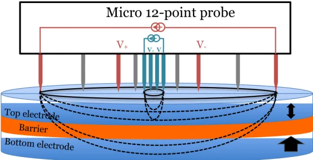
After the discovery of TMR at room temperature in MTJ, people were extensively searching for new types of barrier material. Therefore, there was a need for easy characterization of the fundamental properties of the tunnel junction, which are TMR and the resistance-area product (RA), without having to pattern the device. In 2003, Worledge proposed a novel method called current-in-plane-tunneling (CIPT) for measuring TMR and RA [15]. This model stands on multi-points sheet resistance measurements by varying the probe distance (x). Among the collinear probes, the two outer probes are used to inject current. Then the sheet resistance of the sample is calculated by measuring the induced voltage from the set of inner probes. Depending on the probe distance, when current is injected in the sample, a part of the current flows through the tunnel barrier to the bottom electrode while the remaining part of the current flows in the top electrode, as demonstrated in Figure 1.5.
Figure 1.5: Schematic representation of Micro 12-point probe CIPT technique for measuring RA and TMR of MTJ. Barrier Top electrode Bottom electrode
V
+ VV
-+V1.2 TMR
When the distance is small, the current only flows within the top electrode. Therefore, the measured sheet resistance is the top electrode sheet resistance (RT). For very large probe
distance, the current will be proportionally divided between top and bottom electrodes. In this case, the resistance of the barrier can be neglected and the effective sheet resistance is the parallel combination of the resistance of top and bottom electrodes (RB), i.e. !!!!!
!!!!. A
characteristic length, λ is defined by the equation, 𝜆 = !!"
!!!! , where RA is the
resistance-area product of the tunnel barrier. In the CIPT set up, a special chip with 12 probes is used. The probe spacing (x) is varied by selecting 4 probes out of 12. The sheet resistances of the MTJ with parallel (Rsqlow) and anti-parallel (Rsqhigh) magnetization
orientation are measured for different probe spacing. The MRCIP ratio is given by
𝑀𝑅!"# = !!"
!!"!!! !"!!"!
!!"!"# .
Figure 1.6: (a) Sheet resistances in parallel and antiparallel magnetization orientations and (b) MRCIP of MTJ as a function of probe spacing of CIPT. Figures are redrawn from
Nistor’s thesis [16].
This measured data is then fit as shown in Figure 1.6 (a) and (b) with a model [15] written below to extract RT, RB, TMR and RA.
Probe pitch (x) MR CI P (% ) Rsq Probe pitch (x)
Data and fit_Rsqlow
Data and fit_Rsqhigh RT 𝑅!𝑅! 𝑅!+ 𝑅! 5λ λ 𝑀𝑅!"#= 𝑅!"!!"!− 𝑅 !"!!"! 𝑅!"!"# (b) (a)
𝑅!" = 𝑅!𝑅! 𝑅!+ 𝑅![1 + 𝑅! 𝑅!𝑙𝑛2{𝐾! 𝑥 𝜆 − 𝐾! 2𝑥 𝜆 }] (1.17)
The best fitting is obtained when the probe spacing spans between λ and 5λ.
1.3 SPIN-TRANSFER TORQUE
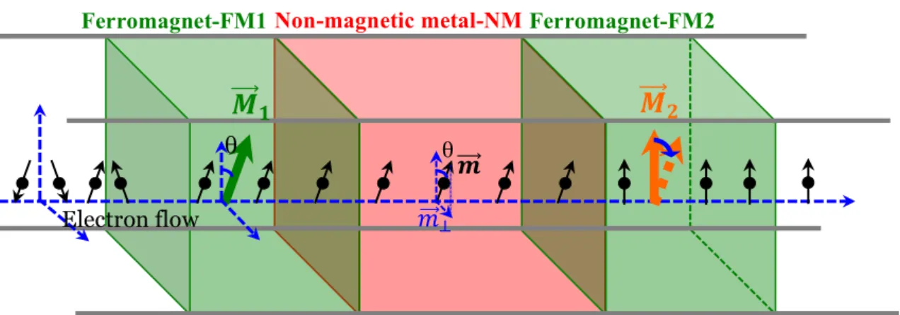
In 1996, Slonczewski [17] and Berger [18] predicted that the magnetization of a ferromagnetic layer can be reversed by a spin polarized current due to spin transfer torque (STT). As already mentioned before, this phenomenon can be viewed as the reciprocal effect of GMR or TMR, in which cases different magnetization alignments of two ferromagnetic electrodes in spin-valve or MTJ influence the electron transport. The STT effect is illustrated in Figure 1.7 using a ferromagnet/non-magnet/ferromagnet spin-valve structure.
Figure 1.7: Schematic representation of spin transfer torque in a spin valve structure.
When an initially unpolarized current flows through the FM1, electron flow gets spin-polarized along the direction of magnetization (𝑀!), due to spin dependent scattering effect as explained in section 1.1. These spin-polarized electrons traverse the non-magnetic layer without losing polarization, as the thickness is less than the spin-diffusion length. After penetrating into FM2, the spins of the electrons are quickly realigned along the magnetization of FM2 (𝑀!) within a very short interval of thickness (≤ 1nm) from the
NM/FM2 interface. As a result, the electrons lose their transverse component of magnetic moment (𝑚!), which is transferred to the magnetization of FM2 due to angular momentum conservation. This spin transfer from the spin-polarized electrons to the local magnetization of FM2 exerts a torque on 𝑀 and tends to align it along the direction of
θ θ
Ferromagnet-FM1Non-magnetic metal-NMFerromagnet-FM2
𝑴
!!!⃗
𝟏 Electron flow 𝑚!!⃗! 𝒎 !!!⃗𝑴
!!!⃗
𝟐1.3 SPIN-TRANSFER TORQUE
spin polarization of the incoming electrons and therefore along the magnetization of FM1. This phenomenon is known as spin-transfer torque (STT) and the analytical expression is derived below.
The transverse component of magnetic moment of electron is expressed as,
𝑚! = −
𝑔𝜇! ℏ 𝑠!=
𝑔𝜇!
2 [𝑚!×(𝑚!×𝑚!)] (1.18) In this equation, 𝑚!and 𝑚!are unit vectors, representing the direction of magnetizations
of FM1 and FM2; 𝑠!is the transverse angular momentum of electron which acts perpendicular to 𝑀! in the plane intersecting both 𝑀! and 𝑀!.
The number of spins reaching FM2 per unit time:
𝑑𝑁𝑑𝑡! = 𝑃𝑑𝑁𝑑𝑡! = 𝑃𝑒𝐼 = 𝑃𝐽𝐴𝑒 (1.19)
Therefore, spin-transfer torque, which is the rate of transferring spin angular momentum to FM2, is Γ!""= 1 𝛾 𝑑𝑚! 𝑑𝑡 = 𝑃 𝐽𝐴 𝑒 ℏ 2[𝑚!× 𝑚!×𝑚! ] (1.20)
The spin-transfer torque is also known as Slonczewski torque, or in-plane torque or damping like torque. In addition to STT, there can be a field-like torque or out-of-plane torque directed perpendicular to the plane of 𝑀! and 𝑀!.
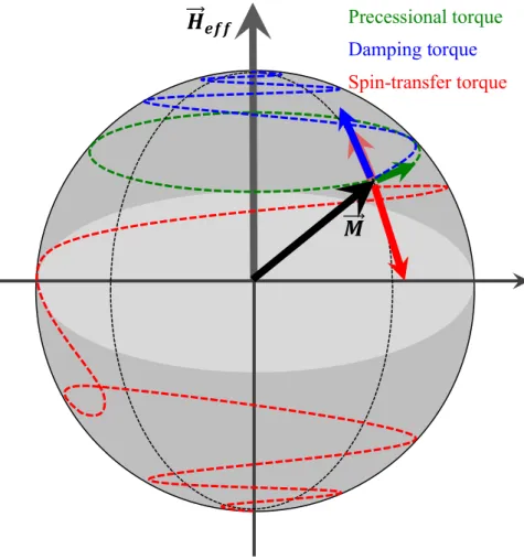
1.3.1 Spin-transfer torque and magnetization dynamics
Under the influence of STT the magnetization dynamics of a ferromagnetic material is governed by Landau-Liftschitz-Gilbert (LLG) equation with the additional term of spin transfer torque. 𝑑𝑀𝑑𝑡 = −𝛾 𝑀×𝐻!"" + 𝛼 𝑀! 𝑀× 𝑑𝑀 𝑑𝑡 − 𝑃 𝐽𝑔𝜇! 2𝑀!𝑒[ 𝑀 𝑀!× 𝑀×𝑝 ] (1.21)
Where 𝑝 is the unit vector of the moment of spin polarized electron flow, 𝐻!""is an effective field combining applied, anisotropy and dipolar field and α is the damping constant. The first, second and third terms of the right hand side of LLG equation are the field torque, damping torque and spin-transfer torque respectively. In the absence of STT and damping, the magnetization continuously precesses around 𝐻 with a frequency
𝜔 = 𝛾𝐻!"". When damping is present, the damping torque acts towards 𝐻!"" from 𝑀 shown by the blue arrow. Therefore, precessional motion under the influence of field torque will be damped as illustrated by blue spiral line in Figure 1.8. When STT is present, two situations can occur. In the first case, when 𝑝 and 𝐻!"" are parallel, STT and damping torques are in the same direction and damp the precession. In the other case, when 𝑝 and 𝐻!"" are anti-parallel, the STT opposes the damping torque. At sufficiently large current density, the effect of damping is cancelled and a stable precession occurs at a certain cone angle. This sustained precession generates radio frequency field. The device is then named as spin-transfer torque oscillator. When the current density is larger than some critical value, the magnetization spirals away from the precessional motion and eventually reverses in the direction opposite to 𝐻!"". After the pioneering theoretical work on STT, the phenomenon was first experimentally observed in 2000 in Co/Cu/Co spin-valves [19], [20].
Figure 1.8: Schematic representations of magnetization dynamics under the influence of
𝑯
!!!⃗
𝒆𝒇𝒇𝑴
!!!⃗
Precessional torque Damping torque Spin-transfer torque
1.4 INTRODUCTION TO STT-MRAM
It is noteworthy that thermal fluctuations at room temperature create a small angle between 𝑝 and 𝑀, which is necessary to trigger the reversal by spin-transfer torque.
1.4 INTRODUCTION TO STT-MRAM
Among all memory technologies, STT-MRAM is particularly promising because of its potential to function as a universal memory in the memory hierarchy. Together with non-volatility, other properties such as, low power consumption, high write speed (few nanoseconds), semi-infinite endurance (>1016 write cycles) and high retention (> 10yrs) make STT-MRAM a good candidate to replace embedded FLASH memory, L2/L3 cache and possibly later DRAM, and to fill up the memory gap between DRAM and solid state drives (storage class memory). The recent advancement of research proves that embedded-STT-MRAM would become a viable memory option for mobile, internet-of-things (IOT) and computer applications [21]–[23]. Moreover, the radiation hardness properties of the materials used in the stack of STT-MRAM makes them useful for space and military application. After 20 years of research and development, the MRAM technology is getting mature enough to find its position in the technology market. All major foundries (Samsung, TSMC, Global Foundries) have announced the ramp up towards volume production in 2018.
1.4.1 Different families of MRAM
The field of MRAM started even before the advent of TMR and STT using the effect of GMR and AMR. After the discovery of TMR in Al2O3 based MTJs, MTJs were used as active memory elements written by magnetic field. A crossbar architecture of memory array was used, where the magnetic field was produced by two sets of orthogonal current lines (Stoner Wolfarth switching). This was the first generation of MRAM classified as field-written MRAM. The first MRAM named Stoner-Wolfarth MRAM had a half-select problem, which is the accidental writing of other unselected memory cells along the word or bit lines. Savtchenko writing solved this problem with a novel design named toggle-MRAM. The memory cell in this design is aligned in 45° with respect to both bit and word lines. The free layer is made up of synthetic antiferromagnetic layer, which is written by applying current to word and bit line in four steps. In 2006, first commercial product of 4-Mb toggle-MRAM was launched by Freescale, which found their position for transportation, industrial and space applications [24].
Figure 1.9: Schematic representations of different families of MRAM.
In this technology, the main bottleneck was scaling down the cell as the write current increases as 1/F2 where F is the lithographic feature size. Another candidate of the field MRAM family is the thermally assisted MRAM (TAS-MRAM), which allows high retention of storage layer with low writing current. The free layer of the memory cell consists of ferromagnetic layer exchange biased with anti-ferromagnetic layer with lower blocking temperature. Applying a heat pulse reduces the exchange bias of the free layer of the selected bits and then with lower current in the field line switches the magnetization. However, the discovery of giant TMR and current induced magnetization reversal by STT, soon replaced this technology by STT-MRAM due to better down size scalability, bit selectivity, simpler design. These features will be discussed in details later in the following paragraphs.
The most recent members of the family of MRAM are three terminal STT-MRAM[25]. In this family, the two candidates are domain wall motion based MRAM and spin-orbit torque MRAM (SOT-MRAM). These devices are still under research and needs to be more mature to reach industrial production. However, they are very interesting as the read and write paths for this memory cell are separated and write current does not flow through the tunnel barrier. This makes the cell extremely endurant during write compared to two terminal STT-MRAM cells. The writing is performed by STT
Thermally Assisted (TAS) STT-TAS
Hx
Hy Hx
Hy
Field-driven Spin Transfer Torque (STT RAM) Perpendicular
Precessional Planar
3-terminal MRAM
Domain Wall-RAM
Spin-Orbit Torque (SOT RAM) (spin-Hall, Rashba)
1.4 INTRODUCTION TO STT-MRAM
expected to be bigger than STT-MRAM, it is also interesting for ultrafast switching (order of pico-second) which makes then potential candidate for replacement of L1 or L2 Cache SRAM.
1.4.2 In-plane vs. perpendicular STT-MRAM
At the beginning of the introduction of STT-MRAM, the MTJs used were with in-plane magnetization. The shape of the bit was elliptical providing shape anisotropy to retain the written bit information. However, after finding perpendicular magnetic anisotropy (PMA) material, the elliptic bits were replaced by circular bit with pMTJs (perpendicular MTJs). The origin of the PMA and different types of PMA materials and their utilization will be discussed later in the following section. pSTT-MRAM is more useful than in-plane STT-MRAM for the following reasons explained below.
For in-plane STT-MRAM the critical switching current (Ico) and thermal stability
factor (Δ) are expressed by
𝐼!" = 4𝛼𝑒 𝜂ℏ 𝑘!𝑇[ 𝜋𝑀!!𝑉 𝑘!𝑇 + Δ] (1.22) Δ = 𝐾!""𝑉 𝑘!𝑇 = 𝜋!(𝑀 !𝑡)!𝑤(𝐴𝑅 − 1) 𝑘!𝑇 (1.23)
where, t is the thickness of the storage layer, w is the width of elliptical cell, AR is its aspect ratio, α and η are Gilbert damping constant and spin-torque efficiency respectively.
For out-of-plane, STT-MRAM the critical switching current (Ico) and thermal stability
factor (Δ) are expressed by
𝐼!" = 4𝛼𝑒 𝜂ℏ 𝑘!𝑇Δ (1.24) Δ =𝐾!""𝑉 𝑘!𝑇 = ( 𝐾! 𝑡 − 2𝜋𝑀!!) 𝜋𝐷!𝑡 4𝑘!𝑇𝑇 (1.25)
Where, D is the diameter of circular bit; Keff, Ki are effective perpendicular magnetic
anisotropy and interfacial anisotropy constant respectively.
The critical switching current for in-plane memory cell is much higher than out-of-plane because of extra term of demagnetizing field. This is due to the fact that during STT induced switching of in-plane magnetized MTJs, in its precessional motion, the storage
layer magnetization has to go out-of-plane against demagnetizing field which costs lot of energy. On the other hand, the barrier, which determines the memory retention, is given by the in-plane shape anisotropy. In other words, for in-plane MTJs, the barrier for switching is much higher than the barrier for retention, which is quite unfavorable in terms of power consumption. In contrast, these barriers are identical for out-of-plane magnetized MTJs. Therefore, for same value of Δ, in-plane memory cell consumes more energy for magnetization reversal. Moreover, easier manufacturability of circular shaped memory element compared to elliptical makes pSTT-MRAM more attractive to realize sub-20nm memory cell.
1.4.3 Properties of material for designing STT-MRAM
The design of the stack for high performance STT-MRAM devices is mainly based on five important requirements as shown in the flow chart above. The first requirement is that the written data retention time should be large (at least 10 yrs). The larger the retention time, the larger is the thermal stability factor. The required values of thermal stability factor (Δ) can be estimated from the following formula of probability of one bit failure in 10years time.
𝑃 𝑡 = 1 − exp [ −𝑁𝑡
𝜏! 𝑒𝑥𝑝(−Δ 300
𝑇 ) (1.26)
In this equation, τ0, N and t represent attempt time of the order of 1 ns, number of bits on
the chip and retention time respectively. T is the temperature in degree Kelvin. Figure 1.10 demonstrates the required values of Δ at room temperature for a memory array to reach a particular value of bit failure rate. For example, the required value of Δ at room temperature is 88 and 94 to obtain 10 years retention time with probability of bit failure
S
TT
-M
R
A
M
d
es
ign
re
q
u
ir
eme
n
ts
High RetentionWriting with low power consumption Readability
Semi-infinite Endurance Integration compatibility and low
1.4 INTRODUCTION TO STT-MRAM
Figure 1.10: Bit failure rate at room temperature and 80°C during 10 years as a function of thermal stability factor at room temperature for different capacities of memory array.
lower than 10-4 respectively for 1Gb and 64 Gb memory array operating at 80°C. Note that in this calculation, it was assumed that the energy barrier remains unchanged as a function of temperature. It is possible to obtain this value of Δ by using perpendicular magnetic anisotropic material. At present, composite type storage layer with two MgO interfaces is used to increase the PMA and therefore Δ of memory cell [26]. A detailed description about PMA materials has been included in section 1.5.
There is a dilemma between writing current and thermal stability factor. The critical switching current (Ico) is proportional to Δ as shown in equations 1.22 and 1.24.
Therefore, improving Δ, also increases Ico,: This is classical a dilemma between retention
and writability. By choosing proper material, which increases spin polarization and reduces damping, as well as by optimizing the structure of the stack, it is possible to reduce the switching current for high values of Δ. Heusler alloys, because of their half-metallic nature, are expected to have 100% spin polarization and also low damping. Researchers are widely searching for Heusler alloys to get these properties at room temperature. However, until now, no successful results were obtained combining high TMR, perpendicular anisotropy and low damping at room temperature. At present FeCoB alloys are the standard material for storage layer, which can provide high TMR and also reasonably low damping constant [27]–[29]. Another approach to increase the STT efficiency is configuring the stack in double-MTJs where storage layer is sandwiched
from both interfaces of the free layer with MgO. A factor 10 reduction of switching current reduction of DMTJ compared to single-MTJ has been predicted by analytical calculation [32]. Another strategy is to reduce the anisotropy by thermal effect [33] or by electric field effect. The second effect, also known as voltage controlled anisotropy (VCMA), can potentially reduce the anisotropy to write the cell with very low current [34], [35].
The reliable and faster reading of a memory cell depends on the TMR values. Large TMR value provides larger signal to separate out the high and low resistance states. In order to discriminate between the two resistances states, the two distributions must be separated by at least 12σ as shown in Figure 1.11, where σ is the standard deviation of the resistance distributions. Moreover, for reliable detection between the bits of low and high states with higher resistance and lower resistance of the distributions, there must be even larger margin about 20σ. This margin again increases with smaller diameter, as the distribution might be broader due to relatively larger edge damage during etching. Therefore, high TMR is necessary for fast and reliable reading. Magnetic tunnel junction with MgO as a barrier can provide large TMR ratio.
Figure 1.11: The distribution of high resistance and low resistance states of a memory array [36].
A maximum TMR ratio of 604% was already obtained using in-plane MTJ [37]. TMR ratio for pMTJs is limited by the thickness of FeCoB layer as PMA of thicker FeCoB diminishes. However, 350% TMR was already demonstrated in pMTJs which ensures faster reading of pSTT-MRAM devices [27]. In addition, for practical industrial MRAM chips, uniformity of the barrier at wafer level is very important since a small drift in the
1.5 PERPENDICULAR MAGNETIC ANISOTROPY : ORIGIN & APPLICATIONS
The endurance of STT-MRAM is defined by the number of read-write cycles that the cell can withstand before dielectric breakdown. The writing voltage of a memory cell should be largely separated from breakdown voltage to ensure an endurance of > 1015 cycles. Therefore, endurance can be improved by reducing the writing voltage. In practical Devices for STT-MRAM, the write voltage is typically set in the range 0.4V to 0.5V while the dielectric breakdown voltage is in the range 1.2-1.5V. Improving the quality of MgO barrier by reducing the number of defects (such as trapped water molecules, vacancies, dislocations etc) increases the breakdown voltage. Similarly the integration process should be optimized to reduce the edge damages while etching the MTJ stack. In the STT-MRAM industry, mastering the barrier quality is well under control. However, the patterning process for ultra-small technology nodes (sub-20nm) and small pitch is still a remaining challenge. Recently, Jimmy J. Kan et al. reported endurance of more than 1015 cycle of 50 ns pulse for 1Mb perpendicular STT-MRAM [38].
Last but not the least criterion is the compatibility of the stack with the STT-MRAM fabrication process. The memory is integrated with CMOS in the back-end-of-line (BEOL) fabrication. Therefore, the stack should be able to endure the BEOL thermal budget which is about 400°C without compromising the magneto-electric properties [39]. The stack should be designed and deposited in such a way that the interfacial roughness at the interfaces between MgO tunnel barrier and ferromagnetic electrodes remains well below the thickness of each individual layers. Otherwise, pinholes and defects in the MgO layer will significantly reduce TMR, PMA and breakdown voltage of memory cells. The pMTJ stacks for STT-MRAM typically consist of multilayers comprising 15 to 25 layers of thickness ranging between 0.2nm and a few nm. The stack should be as thin as possible to reduce the non-volatile etch product during etching, which will improve the yield and decrease the dot-to-dot variability [36].
1.5 PERPENDICULAR MAGNETIC ANISOTROPY : ORIGIN &
APPLICATIONS
The property that causes the magnetization of a ferromagnetic (or anti-ferromagnetic) material to align along a certain direction is called anisotropy. There are several types of magnetic anisotropy contributions: a) magnetocrystalline anisotropy, b) shape anisotropy, c) magnetoelastic anisotropy, d) interfacial anisotropy etc. As this thesis is related to
![Figure 1.4 (b) shows the band dispersion of bcc Fe along [001] direction. From first principle calculation, it has been observed that both majority-spin and minority-spin Δ 2](https://thumb-eu.123doks.com/thumbv2/123doknet/12876096.369653/29.892.120.760.722.979/figure-dispersion-direction-principle-calculation-observed-majority-minority.webp)