HAL Id: hal-01148232
https://hal.archives-ouvertes.fr/hal-01148232v2
Submitted on 10 Dec 2015HAL is a multi-disciplinary open access archive for the deposit and dissemination of sci-entific research documents, whether they are pub-lished or not. The documents may come from teaching and research institutions in France or abroad, or from public or private research centers.
L’archive ouverte pluridisciplinaire HAL, est destinée au dépôt et à la diffusion de documents scientifiques de niveau recherche, publiés ou non, émanant des établissements d’enseignement et de recherche français ou étrangers, des laboratoires publics ou privés.
Resistive switching in silicon suboxide films
Adnan Mehonic, Sebastien Cueff, Maciej Wojdak, Stephen Hudziak, Olivier
Jambois, Christophe Labbe, Blas Garrido, Richard Rizk, Anthony J. Kenyon
To cite this version:
Adnan Mehonic, Sebastien Cueff, Maciej Wojdak, Stephen Hudziak, Olivier Jambois, et al.. Resistive switching in silicon suboxide films. Journal of Applied Geophysics, Elsevier, 2012, 111 (7), pp.074507. �10.1063/1.3701581�. �hal-01148232v2�
Resistive switching in silicon sub-oxide films
Adnan Mehonic1*, Sébastien Cueff2, Maciej Wojdak1, Stephen Hudziak1, Olivier Jambois3, Christophe
Labbé2, Blas Garrido3, Richard Rizk2 and Anthony J. Kenyon1*
1
Department of Electronic & Electrical Engineering, UCL, Torrington Place, London WC1E 7JE, UK
2
CIMAP, UMR CNRS 6252 ENSICAEN, 6 Boulevard Maréchal Juin, 14050 Caen Cedex 4, France
3
MIND-IN2UB, Dept. Electrònica, Universitat de Barcelona, Martí i Fanquès 1, 08028, Barcelona, CAT, Spain
Abstract
We report a study of resistive switching in a silicon-based memristor/resistive RAM (RRAM) device in which the active layer is silicon-rich silica. The resistive switching phenomenon is an intrinsic property of the silicon-rich oxide layer and does not depend on the diffusion of metallic ions to form conductive paths. In contrast to other work in the literature, switching occurs in ambient conditions, and is not limited to the surface of the active material.
We proposed a switching mechanism driven by competing field-driven formation and current-driven destruction of filamentary conductive pathways. We demonstrate that conduction is dominated by trap assisted tunnelling through non-continuous conduction paths consisting of silicon nanoinclusions in a highly non-stoichiometric suboxide phase. We hypothesise that such nanoinclusions nucleate
preferentially at internal grain boundaries in nanostructured films.
Switching exhibits the pinched hysteresis I/V loop characteristic of memristive systems, and on/off resistance ratios of 104:1 or higher can be easily achieved. Scanning Tunnelling Microscopy suggests that switchable conductive pathways are 10nm in diameter or smaller. Programming currents can be as low as 2μA, and transition times are on the nanosecond scale.
1. Introduction
Non-volatile memories based on resistive switching have recently attracted significant attention1. In particular, the two-terminal elements known as memristors2 offer a potential solution to the problem of decreased controllability of charge in semiconductor memories as devices scale to ever-smaller dimensions. First postulated by Leon Chua in in 1971 as the “missing” fourth passive circuit element2, the first practical realisation of the memristor, in titanium dioxide, was not reported until 20083. Such devices have a wide range of potential applications in high-density memories, novel processor architectures, and neural networks. Consequently, the development of a practical CMOS device is a very attractive prospect for integration with current silicon technologies. Proof-of-principle memory systems exploiting memristors have already been demonstrated1, 3-7, typically consisting of multilayer structures in which conductive pathways form under the application of external fields. Titanium
dioxide multilayers, exploiting field-driven redistribution of oxygen ions, were the first reported memristor devices3, but there have also been promising reports of silicon-based resistive switches4, 8. In the latter case, two approaches have been successful: field-driven diffusion of silver ions from metal contacts into amorphous silicon layers5, 8 and switchable conductive pathways on the surface of silicon-rich silica (SiOx) pillars
4
. However, in CMOS processing the diffusion of metallic ions is undesirable, as this could potentially endanger the operation of surrounding electronics. The intrinsic resistive switching of silicon oxide is a more appealing mechanism. The first such system was
demonstrated by Yao et al 4, who reported a switchable silicon conductive path formed on the vertical surface a of silicon-rich silica pillar. However, the operation of such a device is possible only under vacuum due to oxidation of silicon conductive pathways on the device surface under ambient conditions. The authors reported no evidence of high-contrast controllable resistive switching in continuous films of silicon oxide: instead, silicon nanofilaments at vertical surfaces of mesa structures were proposed as the switching elements. In contrast, we demonstrate here a device operating under ambient conditions that relies on switching within a continuous thin film of silicon-rich silica. The device can be cycled between high resistance “OFF” and low resistance “ON” states with a resistance contrast of 10,000 or more. Both states are stable, persisting for at least 120 hours, and likely much longer
2. Experimental details
Our test devices (Figure 1(b)) contain thin (15-120nm) SiOx layers sandwiched between a p-type
silicon wafer and n-type top electrodes (a range of electrode sizes was used – from 6mm×4mm to 125µm×125µm). To address thermal budget issues during fabrication, we investigated two configurations: one with n-type polycrystalline silicon top electrodes, requiring a 950°C anneal to optimise conductivity, and a second with indium tin oxide (ITO) electrodes, deposited at room temperature. The former is readily integrated with front-end CMOS processes; the latter allows memristors to be integrated onto existing device layers without high temperature processing. The SiOx layers were deposited by magnetron co-sputtering onto p-type, B-doped silicon (100)
pure argon plasma. Layer thicknesses between 15nm and 120nm (measured by spectroscopic ellipsometry) were used for different devices, and excess silicon content was between 11 and 30at% for different samples (measured by XPS: Perkin-Elmer PHI-5500). Results reported here were from samples containing 11at% excess Si. Samples were annealed at 900°C or at 500°C post-deposition in an argon atmosphere. The initial sample annealing temperature had little effect on the switching behaviour of the devices.
For one batch of samples, 185nm of n-type silicon (phosphorous doped, resistivity 10mcm) was deposited on top of the SiOx layer by Low Pressure Chemical Vapour Deposition (LPCVD). After
growth, samples were annealed at 950°C for 30 minutes in nitrogen to activate the dopants and achieve a final resistivity of 1mcm. After a buffered HF dip to remove surface oxide, 100nm of chrome was sputtered onto the front side, photoresist spun on, and the sample exposed with a chrome-on-glass mask. The mask contained a number of different electrode sizes – from 6mm×4mm to 125µm×125µm. The photoresist was developed, then the exposed chrome etched. Removal of the remaining photoresist was followed by a buffered HF etch and the samples were etched in TMAH, 25% solution at 60°C, for 40 sec. Finally, the chrome was etched, and the samples rinsed and blow-dried in N2.
A second set had 70nm-thick ITO layers deposited by sputtering, followed by photolithographic contact definition using the same mask as for set 1. The ITO layer was etched using hydrochloric acid. Chrome-gold Ohmic contacts were provided on the back sides of all wafers by evaporation (10nm Cr, followed by 100nm Au).
An asymmetric structure (n-type top electrodes (n-Si or ITO); p-type substrate), allows us to define two regimes in our MOS structure. Applying a negative potential to the top electrode allows higher currents to flow (negative bias); a positive potential results in lower currents (positive bias). In similar oxide based resistive systems, externally controlled current compliance has been required for
successful operation. High current passing through thin oxide film could cause irreversible hard breakdown thus leading to device failure. An asymmetric design allows us to cycle the device without the need for external current compliance.
I/V and I/t measurements were performed using a Keithley 4200 Semiconductor Characterisation System and a Signatone probe station. STM measurements were taken using a Nanosurf easyScan 2 Scanning Tunnelling Microscope. Atomic Force Microscopy (AFM) measurements were taken using a Veeco Dimension 3100 AFM operating in contact mode.
All experiments were performed in ambient conditions in an open laboratory. All shown results are preformed on the devices with the top ITO contact, 37nm thick active layer and 11at% excess Si unless otherwise specified.
3. Results and discussion
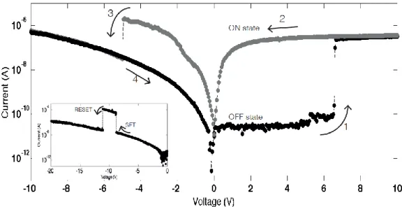
3.1. Current – voltage characteristicsFigure 1. (colour online) (a) IV characteristics (125µm×125µm top electrode). The black line in the positive bias shows a transition from OFF to ON state. The grey line shows a full ON state afterwards. The grey line in the negative bias shows a transition from ON to OFF state and the black line shows a full OFF state afterwards. Inset: Logarithmic representation. (b) Device schematic. (c) ON and OFF states dependence on increasing
temperature. (d) Switching cycles using voltage pulses of +20V, -20V and +2V for setting, resetting and reading, respectively. (e) IV characteristics for device with poly-Si top contact (30at% excess Si, 37nm thick layer, 125μm x 125μm contact size).
Figure 1(a) shows typical I/V results (contact size: 125µm×125µm). Hysteresis is evident in both positive and negative bias, and the data show the pinched hysteresis curve characteristic of memristive systems. In positive bias, the initial high impedance (OFF) state switches to a low impedance (ON) state at a threshold voltage (black line in the positive bias). This is the “set” process. Reducing the voltage below threshold does not switch the device to its initial state, and much larger currents flow (grey line). Resistance contrast between the two states is up to sixorders of magnitude in devices studied to date; four orders are typical. Transitions between states are abrupt (ie faster than the sampling time of our measurement) and do not depend on voltage sweep speed. The results shown are obtained with an acquisition time of around 15ms per point (the maximum resolution of our equipment), which is equivalent to a sweep rate of 3.33 Vs-1 with 300 points sampled.After switching, the device stays in the low impedance state until a negative bias is applied and certain critical current is reached. Although the low resistance to high resistance (“reset”) switching process can be achieved in both polarities, the negative bias is much more efficient as higher currents can be achieved with lower voltages than in positive bias. A sharp drop in current can be seen (grey line in negative bias) when the required current level is reached under negative bias. Note in the example shown in figure 1a that the device returns to the initial high resistance OFF state following the reset process – in some cases it is possible to return the device to a partially OFF state with an intermediate resistance (see figure 2). The formation (“set”) process can be achieved by again applying a positive bias. We note that the set process is also achievable under negative bias (Figure 2 inset), but its occurrence is less likely (and normally occurs only for larger contacts) than in the case of positive bias.
Figure 2. IV characteristics (125µm×125µm top electrode). Inset: Unipolar switching for device with ITO contact (250μm x 250μm contact size)
Samples with silicon top contacts exhibited switching behaviour that was qualitatively similar to those with ITO contacts (Figure 1e), but higher reset currents were required, leading to reduced device endurance. We believe that this can be attributed to an additional annealing step at 950°C required to maximise the conductivity of the n-type poly-Si layer. This is likely to produce a high density of silicon nanoinclusions within the film as a result of phase separation, allowing strong conductive pathways to form. Future implementations of all-silicon memristors will therefore require careful control of the processing thermal budget.
Set and reset voltages can vary from the values shown in Figure 1a, depending on the history of the devices (duration and magnitude of the last applied voltage bias). However, short voltage pulses of ±15V or greater almost always trigger switching in healthy devices. These switching processes are repeatable, and the states stable for at least 120 hours at room temperature. Figure 1(d) illustrates sequential cycling between high and low resistance states (device programming). For the results shown in Figure 1(d) a programmed sweep mode was used with a sweep speed of around 50ms per point (the maximum resolution of our equipment in this mode). The applied voltages were: +20V (set), -20V (reset), and +2V (read). In the best devices programming can be achieved using 10V pulses as short as 90ns (the limit of our equipment resolution – for these measurements a stand-alone
pulse generator was used, rather than the Keithely 4200). Reset current in these devices can be up to 100μA (typical is around 10μA, and in the best devices this can be as low as 2μA (Figure 2)), which is still sufficiently low for memory applications. The read operation uses approximately an order of magnitude less current in the ON state. The variations in reset current are likely an effect of non-homogeneous film deposition. Material optimisation should provide better uniformity of reset currents and programming voltages.
Figures 1(c) shows conduction dependence on temperature in both ON and OFF state. Result shows typical semiconductor behaviour (resistance decreases with increased temperature), suggesting no metallic conduction in the ON state. Temperature increase does not affect the OFF state.
Figure 2 shows an IV curve for a sample with an ITO top contact in which the reset process puts the device into a partially OFF state; although the resistance is reduced by approximately one order of magnitude by the reset pule, the device does not return to the initial fully OFF state. This suggests the possibility of multi-level operation of devices.
The ON current does not show a clear tendency to scale with contact size (we tested this with the 3 contact sizes of 125µm×125µm, 250µm×250µm and 500µm×500µm), suggesting carrier transport via individual conductive pathways. Contrary to other reports, in which switching is attributed to ionic diffusion from metallic contacts9, the switching in our device is an intrinsic property of the silicon-rich silica layer, so we hypothesise that the conductive pathways are related to the excess silicon content. In addition, we note that indium tin oxide is known to be very good diffusion barrier10, further supporting our conclusion that metallic diffusion is not the source of the resistive switching.
Moreover, devices with poly-silicon contacts show very similar resistive switching behaviour (Figure 1(e)). When devices are heated up to 200°C during test, the conductivity in the ON state shows a reversible increase, confirming the non-metallic nature of the conduction path (Figure 1(c)). As the current is determined by the conductive pathway rather than the availability of carriers from the substrate, we conclude that the pathways are silicon, rather than diffused metal ions from the ITO top contact, or from contamination of the active layer. Contrary to this, systems exhibiting metallic filament conduction show a decrease in the ON state conduction with increasing temperature due to filament melting11.
Also shown in Figure 2 (inset) is unipolar switching of the device under negative bias. Both set and reset processes can be seen, with reset occurring once the current has reached a critical value. The switching process is thus inherently unipolar.
Figure 3. (a) IV curve (in positive bias) shows three distinct levels (two set processes and competing process) (b) IV curve (in negative bias) shows three distinct levels (two reset processes and competing process).
We note that the both ON read current and reset current could be increased if much larger contacts are used (2mm×2mm or larger). In this case it is likely that a number of parallel conduction paths are formed. Further evidence of multi-level switching is shown in Figure 3. In this case, three distinct levels, together with competing set/reset processes are shown in Figure 3(a) and 3(b).
3.2. Current – time characteristics
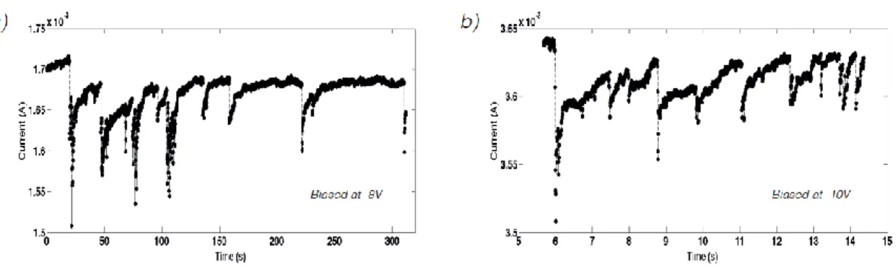
Figures 4(a) and 4(b) show current-time graphs under constant voltage biases of -8V and -10V for the 2mm×2mm contact: it is evident that formation (set) and destruction (reset) processes act in
opposition. In the case of larger contacts, it is likely that multiple conduction paths are formed, resulting in increased reset negative voltage and current. Clear transitions between two states can be seen with rapid current drops (up to 10%) followed by slower, exponential, increases indicating multiple conduction paths where switching occurs in one or a few paths while other paths remains intact. Recovery speed is proportional to the applied voltage: the average time constant decreases from 10sec to around 0.5sec on changing the bias from -8V to -10V. Higher negative voltages reset the device without repetitive transitions to the ON state. However, the ON state is stable if the bias is lower than 6V. We distinguish two conditions: high field and low current (positive bias) in which pathway formation is favoured, and high field and high current (negative bias) in which destruction
dominates. We therefore propose a switching mechanism based on competing field-driven formation and current-driven destruction of conductive pathways.
Figure 4. Current-time graphs under a constant voltage bias of (a) -8V and (b) -10V.
3.3. Impedance spectroscopy and conduction mechanism
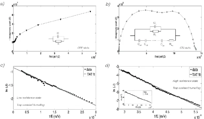
Impedance Spectroscopy1, 12 reveals different conduction mechanisms in ON and OFF states, and is used to examine the nature of conducting path. In the OFF state, a single arc suggests an equivalent circuit model with a single parallel capacitor and resistor (R = 2.811010Ω, C = 2.6110-12F). This high resistance is governed by the bulk properties of the SiOx layer. However, in the ON state, two
clear arcs are seen, suggesting additional parallel resistances and capacitances appearing in series. This is consistent both with formation and destruction of conductive pathways, and with previous studies of carrier transport in such films. The latter can be modelled as shown in the inset of Figure 5b (R1 = 1.68106Ω, C1 = 1.7210-10F; Req = 2.58106Ω, Ceq (equivalent capacitance of series capacitors)
= 3.0310-10F). The imaginary part of the impedance remains negative at frequencies between 1 Hz and 107 Hz, suggesting no inductive behaviour, which would be typical for metallic filaments.
Figure 5. Cole - Cole plots with equivalent circuits under 1V in (a) OFF state and (b) ON state. Trap assisted tunnelling fit in (c) ON (low resistance) state and (d) OFF (high resistance) state (Inset: Fowler-Nordheim tunneling fit in OFF state).
The trap-assisted tunnelling dominates the conduction mechanism in both ON (low resistance) and partially OFF states (high resistance) (here, partially off refers to the black line in reverse bias in Figure 2; in the fully OFF state, there is insufficient current to measure conduction). Figure 5(d) shows data fit in the partially OFF state with the trap assisted tunneling model. The obtained trap depth is 0.52eV.A reasonably good fit (especially at higher fields) can also be achieved with the Fowler-Nordheim tunnelling (F-N) model, as shown in the inset of Figure 5(d). In this case, a barrier height of 0.66eV is obtained which is consisted with literature results reported by DiMaria13.
ON state conduction is modelled best using trap assisted tunnelling for all applied fields (Figure 5(c)). The obtained value for trap depth is 0.086eV. In order to make sense of this result, we note that it is likely that the matrix in between the silicon nanoinclusions will be a suboxide of silicon with a much smaller band gap than stoichiometric SiO2, resulting in a much lower barrier height – intermediate
between the band offset of the Si/SiO2 interface, and zero. A chain of nanoparticles is formed, and
transport proceeds via trap-assisted tunnelling (TAT) between adjacent nanoparticles14,15. The larger trap depth in the partially OFF state can be ascribed to a reduction in the stoichiometry of gaps in the
conductive pathway following removal of nanoinclusions by Joule heating. The trap depth here increases, moving towards a value close to the Si/SiO2 band offset. Note that we did not observe
Fowler-Nordheim tunnelling in devices in the fully ON state.
3.4. Scanning Tunnelling Microscopy & Atomic Force Microscopy
Figure 6. (colour online) (a) STM I/V curves for the edge point (b) Atomic force microscopy scan of the surface top side showing surface features attributed to the tops of growth columns (c) Scanning tunnelling microscopy scan of a sample surface (different area to that in b)) showing enhanced conductivity at column edges (d) Schematic of columnar structure of switching film and switchable site.
It is well established that films grown by sputtering often exhibit columnar or granular growth16. Boundaries between adjacent columns can extend through the whole thickness of the film, effectively connecting the top and bottom of the active layer. Atomic Force Microscopy (Figure 6(b)) of sample surfaces indicated periodic 5-10nm high circular dome-shaped surface features that varied in diameter from 10nm to 50nm. STM of these structures showed high conductivity at the edges of the features, and low conductivity at the centre (Figure 6(c)). Such pathways are around 5-30nm in diameter, suggesting that devices may be scaled down to the nanometre dimensions to achieve very high levels
of integration. Figure 6(a) shows I/V measurements of the two regions, highlighting the difference in conductivity. Figure 6(d) is a schematic of the film structure, showing columnar structures with silicon nanoinclusions nucleating at column boundaries. Such a structure is consistent with both AFM and STM results.
3.5. Switching model
In order to explain the memristive behaviour of our devices, we first note that silicon-rich silica is a metastable material that readily segregates into silicon and silicon dioxide17, 18. It contains a high concentration of oxygen vacancies19, which can be driven by high temperature annealing and consequent diffusion of vacancies and silicon to form silicon nanoclusters. In the initial stages of annealing, sub-nanometre clusters nucleate at oxygen vacancies20, increasing in number and growing by Ostwald ripening at longer times and/or higher temperatures as silicon diffuses. We propose that voltages applied across our devices drive oxygen vacancy migration, producing a field-driven phase separation of the active layer21. This separation is enhanced by structural defects such as nano-scale cracks or inclusions18; significantly, films grown by sputtering typically exhibit columnar or granular growth16; boundaries between adjacent growth columns constitute structural defects that can nucleate phase separation. The rate of nucleation, as well as the number density and size of silicon
nanoinclusions produced by the migration of oxygen vacancies, will increase with applied field until a critical point at which percolation pathways can be formed along the column boundaries
(corresponding to the “set” process). Current transport in devices in the ON state is by trap assisted tunnelling, suggesting that conductive pathways through our material are not continuous filaments, but instead a sequence of separate but neighbouring silicon nanoinclusions (analogous to aggregated oxygen vacancies). The low activation energy in ON state (found for the TAT fit) is typical for conduction through oxygen vacancy defects. Such a low value is understandable if we assume that transport is through a semi-continuous array of adjacent silicon nanoinclusions in a sub-oxide matrix. The stoichiometry of the inter-inclusion matrix varies with applied field and Joule heating, with a more stoichiometric matrix (in the case of a partially OFF device) yielding a higher barrier height than for a very Si-rich matrix.
The switching process is intrinsically unipolar (Figure 2), though we employ bipolar operation as this enables more stable programming.
The proposed process is shown schematically in Figure 7.
Figure 7. Schematic of one cycle process. (a) Initial OFF state before applying the electric field, showing as-grown silicon nanoinclusions nucleated at oxygen vacancy sites. (b) ON state after the chain formation, showing extra silicon nanoinclusions produced by field-driven migration of oxygen vacancies. (c) Annihilation process due to Joule heating. (d) Silicon and oxygen distribution at the weak point.
Although Joule heating is the main driving force for the reset process, the electric field undoubtedly plays an important role. It is known that the silicon/silica interface is more favourable for the formation of oxygen vacancies22 and thus more porous. Consequently, it is more likely that the position of the weak (switching) point is near the substrate/silica interface. As the oxygen vacancies behave as positively charged species, vacancies would be pushed towards the substrate during the set process (positive bias), recovering the broken path. In the reset process (negative bias) energy from the high local Joule heating overcomes the binding energy of vacancies, and the electric field consequently pushes them towards the top electrode, rapturing the conduction path.
4. Conclusion
In conclusion, we report a study of resistive switching in silicon-rich silicon dioxide films grown by co-sputtering. Our results suggest that conductive pathways are formed at grain boundaries by the field-driven nucleation of oxygen vacancies. Such pathways are not continuous, but are chains of silicon nanoinclusions separated by a highly sub-stoichiometric oxide matrix. A combination of applied field and Joule heating controls the distribution of oxygen vacancies, which is reflected in changes in the device resistance of four orders of magnitude or more. Our memristive RRAM device differs from those previously reported by not requiring diffusing metallic contacts5, and not being limited by surface conduction to vacuum operation4. The resistive states are stable,switching pulses can be 90ns or shorter, and switching currents are around 10µA. Such devices are very promising for application in memristive systems such as high-density semiconductor memories. We note that further investigation (underway) should yield more detailed insight into the microscopic switching
mechanism.
References
1. P. Heremans, G. H. Gelinck, R. Muller, K. J. Baeg, D. Y. Kim and Y. Y. Noh, Chemistry of Materials 23 (3), 341-358 (2011).
2. L. O. Chua, IEEE Transactions on Circuit Theory CT18 (5), 507-& (1971).
3. D. B. Strukov, G. S. Snider, D. R. Stewart and R. S. Williams, Nature 453 (7191), 80-83 (2008).
4. J. Yao, Z. Z. Sun, L. Zhong, D. Natelson and J. M. Tour, Nano Letters 10 (10), 4105-4110 (2010).
5. S. H. Jo, K. H. Kim and W. Lu, Nano Letters 9 (1), 496-500 (2009). 6. A. Sinitskii and J. M. Tour, ACS Nano 3 (9), 2760-2766 (2009).
7. M.-J. Lee, C. B. Lee, D. Lee, S. R. Lee, M. Chang, J. H. Hur, Y.-B. Kim, C.-J. Kim, D. H. Seo, S. Seo, U.-I. Chung, I.-K. Yoo and K. Kim, Nature Materials advance online publication (2011).
8. S. H. Jo and W. Lu, Nano Letters 8 (2), 392-397 (2008).
9. R. Huang, L. J. Zhang, D. J. Gao, Y. Pan, S. Q. Qin, P. R. Tang, Y. M. Cai and Y. Y. Wang, Applied Physics a-Materials Science & Processing 102 (4), 927-931 (2011). 10. C. M. Liu, W. L. Liu, W. J. Chen, S. H. Hsieh, T. K. Tsai and L. C. Yang, Journal of the
Electrochemical Society 152 (3), G234-G239 (2005).
11. F. El Kamel, P. Gonon, C. Vallee, V. Jousseaume and H. Grampeix, Applied Physics Letters 98 (2), 023504 (2011).
12. E. Barsoukov, MacDonald, J. Ross, Impedance Spectroscopy: Theory, Experiment, and
Applications. (John Wiley & Sons, Inc., Hoboken, New Jersey, 2005).
13. D. J. Dimaria, D. W. Dong, C. Falcony, T. N. Theis, J. R. Kirtley, J. C. Tsang, D. R. Young, F. L. Pesavento and S. D. Brorson, Journal of Applied Physics 54 (10), 5801-5827 (1983). 14. M. Porti, M. Avidano, M. Nafria, X. Aymerich, J. Carreras and B. Garrido, Journal of Applied
Physics 98 (5), 056101 (2005).
15. O. Jambois, Y. Berencen, K. Hijazi, M. Wojdak, A. J. Kenyon, F. Gourbilleau, R. Rizk and B. Garrido, Journal of Applied Physics 106 (6), 063526 (2009).
16. M. T. P. McCann, D. A. Mooney, M. Rahman, D. P. Dowling and J. M. D. MacElroy, Acs Applied Materials & Interfaces 3 (2), 252-260 (2011).
17. L. A. Nesbit, Applied Physics Letters 46 (1), 38-40 (1985).
18. G. A. Kachurin, K. S. Zhuravlev, N. A. Pazdnikov, A. F. Leier, I. E. Tyschenko, V. A. Volodin, W. Skorupa and R. A. Yankov, Nuclear Instruments & Methods in Physics Research Section B-Beam Interactions with Materials and Atoms 127, 583-586 (1997). 19. S. Cueff, C. Labbe, B. Dierre, F. Fabbri, T. Sekiguchi, X. Portier and R. Rizk, Journal of
Applied Physics 108 (11), 113504 (2010).
20. C. R. Mokry, P. J. Simpson and A. P. Knights, Journal of Applied Physics 105 (11), 114301 (2009).
21. A. Sarikov, V. Litovchenko, I. Lisovskyy, I. Maidanchuk and S. Zlobin, Applied Physics Letters 91 (13), 133109 (2007).
22. A. X. Chu and W. B. Fowler, Physical Review B 41 (8), 5061-5066 (1990).
Acknowledgements
We acknowledge the valuable assistance provided by Steve Etienne (cleanroom processing). AM was supported by a UCL Overseas Research Scholarship. Funding was provided by EPSRC.