HAL Id: hal-01887199
https://hal.archives-ouvertes.fr/hal-01887199
Submitted on 3 Oct 2018
HAL is a multi-disciplinary open access
archive for the deposit and dissemination of
sci-entific research documents, whether they are
pub-lished or not. The documents may come from
teaching and research institutions in France or
abroad, or from public or private research centers.
L’archive ouverte pluridisciplinaire HAL, est
destinée au dépôt et à la diffusion de documents
scientifiques de niveau recherche, publiés ou non,
émanant des établissements d’enseignement et de
recherche français ou étrangers, des laboratoires
publics ou privés.
Adiabatic capacitive logic: A paradigm for low-power
logic
Gaël Pillonnet, H. Fanet, S. Houri
To cite this version:
Gaël Pillonnet, H. Fanet, S. Houri. Adiabatic capacitive logic: A paradigm for low-power logic.
2017 IEEE International Symposium on Circuits and Systems (ISCAS), May 2017, Baltimore, United
States. �10.1109/ISCAS.2017.8050996�. �hal-01887199�
Adiabatic Capacitive Logic:
a paradigm for low-power logic
G. Pillonnet, H. Fanet
Univ. Grenoble-Alpes, CEA-LETI Grenoble, France
S. Houri
Tech. Univ. Delft Delft, The Netherlands Abstract—Although CMOS technology scaling combined with
efficient frequency and voltage scaling strategies offer femto Joule per logic operation, energy consumption remains orders of magnitude above the limit given by information theory. To alleviate this inherent energy dissipation, this paper introduces a new paradigm: the adiabatic capacitive logic. Based on adiabatic operation, the principle also relies on a smooth capacitance modulation to achieve a quasi zero-power logic dissipation. This method limits leakage by using metal-metal junctions instead of semiconductor one. It also avoids dynamic power consumption by adiabatic transitions. The contact-less operation promises a better reliability compared to logic based on nano-mechanical relays.
Keywords—adiabatic logic; mems; low-power; variable capacitor I. INTRODUCTION
The classical combinational logic approach is based on the charge and discharge of the equivalent gate capacitor Co of the
nth gate by a constant voltage supply V
cc through the resistive
channel Ron of the n-1th gate as shown in Fig. 1.a. This
particular energy transfer for coding a logic state at the operating frequency fsw leads to an inherent power dissipation
equal to CoVcc2fsw due to the charge-discharge cycle. Furthermore, the inherent leakage of semiconductor junctions used in CMOS transistors induces a static power loss IleakVcc
which is linked to the threshold voltage Vth and the supply
voltage ratio. To balance the dynamic and static power losses, the designer has to find the best trade-off between the technology {Vth,CL,Ron} and design {Vcc,fsw} parameters.
Unfortunately, the energy per operation of the classical CMOS logic is 6 to 10 decades higher than Landauer’s theoretical limit of kTln2 [1]. CMOS scaling such as modifying the on-off ratio does not drastically change this previous statement. It is
therefore clear that there is room for a new logic coding concept to dramatically reduce the power consumption of the present CMOS digital core. To limit the dynamic loss,
CoVcc2fsw, the loss-less transformation called adiabatic logic was
proven using a CMOS transistor as shown in Fig. 1 [2].
The principle of adiabatic logic is to charge and discharge capacitors at constant current generally by applying a ramping supply voltage instead of a constant voltage. By using this principle, the active power dissipation becomes can be expressed as [1]: sw PCf V C T RC P 2 0 0 = (1)
where R is the on-state resistance of the switch and T is the duration of the power supply ramping. A large reduction is possible if T larger than the product RC0. Unfortunately using CMOS technology, a non-adiabatic dissipation C0Vth2 appears due to the threshold voltage Vth of the transistor. Due to a non-adiabatic threshold voltage effect, this technique reduces by a factor of 10 if Vth is assumed to be a third of the supply voltage.
But the static loss is not suppressed as it is still based on semiconductor technology and follows the Shockley law. To reduce the static loss, electromechanical relays [3] seem to be a promising approach as their leakage current is only due to surface leakage effects instead of following the Shockley law [4]. In other words, the channel is a metal-to-metal contact instead of a semiconductor barrier [5]. Unfortunately, their poor mechanical reliability, low switching frequencies, and relatively high operating voltages have been highlighted in literature [6,7].
This paper propose a new paradigm to design a combinational ultra-low-power logic from these two existing solutions combined with a new contact-less approach.
II. ADIABATIC CAPACITIVE BASED LOGIC
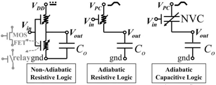
Fig. 1 shows the basic comparison of a resistive based
inverter gate in non-adiabatic and adiabatic operation. Our approach is called adiabatic capacitive logic (ACL). The output load Co represents the capacitance of the next gates and the
interconnect. The timing sequence is similar to adiabatic logic where the power supply is a trapezoidal voltage VPC called the
power clock divided in four phases. In our approach, the elementary device is a variable capacitor (VC) called CDS
which is controlled by an independent gate terminal VG. For a
Negative-type VC device (NVC) the capacitor value decreases when the gate voltage VG increases as shown in Fig. 2.
VPC
V
outC
o gndNVC
V
in Adiabatic Capacitive Logic VDDV
outC
o gndV
in Non-Adiabatic Resistive Logic relay MOS FET VPCV
outC
o gndV
in Adiabatic Resistive Logic (our proposal)Fig. 1 Basic principle of the Adiabatic Capacitive Logic for an inverter gate
The variation is the opposite for a positive-type CV (PCV). The CDS(VG) transfer function is given by the technology of the
device implementation. By operating before the electrical contact as a VC, the physical contact in the device between the
two electrodes S and D can be avoided thus improving the device mechanical reliability and avoiding the need for a low contact resistance. Another advantage is the absence of a non-adiabatic dissipation [4]. VG CDS CH VH CL VL
PVC
S D GNVC
Fig. 2 Example of variable capacitor (VC) device characteristics
For an inverter or a buffer gate, shown in Fig.3, the electrical equations are:
)
(
)
(
)
(
)
(
t
Ri
t
V
V
V
t
V
PC=
+
DS in+
out (2a)dt
V
dC
t
V
dt
dV
V
C
t
i
DS in DS DS in DS)
(
)
(
)
(
)
(
=
+
(2b)(
)
V t dCdtV dt t dV C V C t i e out out out i out e ) ( ) ( ) ( ) ( ) ( = + + (2c)Where VDS, Ce, Ci and i are the voltage across the variable capacitor, the input capacitance value of the next stages (no-constant), the interconnect capacitance and the current flowing from the supply voltage respectively.
C
e(V)
V
outC
e(V)
gndC
iR
V
inC
DS(V
in)
VPCV
out gndC
iR
V
inC
DS Inverter Bufferi(t)
VPCFig.3 Simplified electrical model of the gate
If the voltage drop across resistor R is neglected and if Ce is supposed constant, it is easy to solve system given in equation (2). Therefore the output logic level is fixed at each given time can be expressed as:
PC i e in DS in DS out V C C V C V C V + + = ) ( ) ( (3)
The input voltage variation Vin leads to a capacitance
variation CDS, then the gate, composed of a capacitor bridge
divider, is modulated and transfers (or not) the power clock amplitude to the output node. To distinguish the low and high logic states, the capacitor variation has to be higher than the
load capacitor. In the classical approach, the channel resistance of the transistor is modulated between RON and ROFF states
which then create a resistive bridge between Vcc and the output.
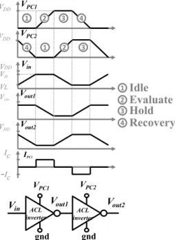
In digital adiabatic systems, gates have to be cascaded and the adiabatic condition has to be satisfied [8,9]: during ramp-up and ramp-down of the power-clock voltage, input voltages have to be stable. Fig. 4 shows the waveform of the main signals which is similar to an adiabatic logic sequence. Four equally spaced power clocks are needed to cascade indefinitely the APL gates. The power clock of the next gate is delayed by a quarter of a period e.g. the evaluation phase of nth gate is the hold phase for the n-1th gate.
VPC1 gnd VDD VPC1 VPC2 Vin Vout1 Vout2 VH VL 1 2 3 4 1 2 3 4 1
Idle
2Evaluate
3Hold
4Recovery
Vin Vout1 VPC2 gnd Vout2 Ic IPC1-
Ic ACL inverter ACL inverter VDD VDD VDD VDDFig.4 Pipelined Adiabatic Capacitive Logic Architecture
To satisfy the adiabatic condition, the basic gate architecture depicted Fig.3 has to be modified by introducing a supplementary variable capacitor in order to maintain the output voltage in the hold phase when the input is decreasing. Fig. 5 shows the proposed topology for the inverter gate with the complementary input logic state. This technique allows the logic evaluation of the n+1th gate in the third phase without losing the logic state in nth gate. Reset switches with a lower timing constraint have to be introduced to regularly set the static voltage as no DC electrical path exists.
V
PCV
outC
ognd
V
inC
oV
inV
outRST
RST
By using only NCV and PCV devices, all combinational logic can be generated in ACL.For example, Fig. 6 shows the OR and NOR logical parts of the gates. Notice the gate does not need any complementary device as in the resistive logic (Fig. 1). The complementary logic state is achieved by the charge/discharge of the output capacitor by the same device.
V
PCV
outC
oV
in,1gnd
V
in,2OR
V
PCV
outC
oV
in,1gnd
V
in,2NOR
Fig. 6 Basic combinational logic functions in ACLIf the capacitance transfer functions CP,N(VG) are correctly
chosen, VL and VH values code distinguished low and high
logic states during the third phase. As the power clock
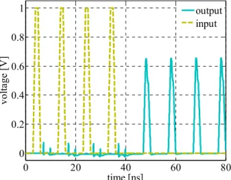
regenerates the signal amplitude at each stage, the logical states amplitudes are maintained over the whole logic depth. The PC current i(t) is a quasi-square waveform as it provides the energy to charge the output capacitance in phase 2 then give back this energy in phase 4. This behavior implies a charge recovery supply. 0 20 40 60 80 0 0.2 0.4 0.6 0.8 1 time [ns] vo lta ge [V ] output input
Fig. 6 Simulations of output signal in a series of 4 inverters
To prove the ability to code logic states and maintain this level during the holding period, Fig.6 shows a particular example with an arbitrary voltage to capacitor transfer function. The signals called input and output are the input signal and output signal of a four adiabatic capacitive inverters. The binary input word is “1 1 1 1 0 0 0 0”. The transfer functions of PVC and NVC capacitors are inspired from Fig.2 and are given by the following relation:
)
(
tanh
)
(
tanh
TN G DS TP G DSV
V
b
D
C
C
V
V
a
B
A
C
−
−
=
−
+
=
(4)A, B, C, D, a, b, VTP, VTN are adjusted parameters. The
simulation uses the following values:
V
V
V
V
b
a
V
V
fF
C
fF
C
C
TN TP PC DS DS2
.
0
;
3
.
0
;
50
;
10
;
1
;
01
.
0
;
1
min max max 0=
=
=
=
=
=
=
=
III. USE OFELECTROMECHANICALDEVICES
The key challenge is being able to define the scalable
hardware necessary to implement the elementary CV devices. To modulate capacitor values, the plate surface, dielectric thickness between the two electrodes and permittivity could be used. Fig. 7 shows a viable candidate for CV implementation, where the gap between the MEMS electrodes is modulated by electrostatic force applied through the gate voltage. Hence the
CDS is modulated by the gate voltage which is electrically
isolated from the drain and source terminals. The variable gate capacitance CG of the nth gate is then the load Co of the n-1th
gate. Other physical phenomena could also be used such as piezo or ferroelectric materials. The main objective is to achieve a sub-volt actuation and to reduce the power clock amplitude in order to decrease the adiabatic loss due to the resistive path R and the loss due to the mechanical damping effect. G gnd S D CG C DS S D G CDS CG gnd insulator stopper contact ge gs thickness ηge
Fig. 7 NVC device implementation using electrostatic MEMS
It is very important to notice that in this device implementation, the complementary device are not needed to hold the logic state during the holding state. The hold function is created in the variable capacitor CDS itself thanks to the residual electrical field. In order to calculate output signals and dissipated energy in series of four buffers, it is necessary to include the electromechanical model of the variable capacitor instead of writing the transfer function of the capacitor. The mechanical equation is written as:
(
)
(
)
2 2 0 2 2 0 2 22
2
g
x
V
S
x
g
V
S
kx
dt
dx
Q
km
dt
x
d
m
s DS G e G G−
+
−
=
+
+
ε
αε
(5)The variables x, m, k, Q, Ɛ0, SG, αSG, ηge are the displacement of the beam, the mass of the beam, the spring constant, the quality factor of the beam, the vacuum permittivity, the areas of input and output capacitors, and the thickness of the stopper respectively.
It is now interesting to define normalized variables:
k
m
t
S
kg
V
g
g
r
Q
V
V
V
t
t
t
g
x
x
G e e s e/
/
/
~
1/
/
~
/
~
/
~
0 0 3 0 0 0=
=
=
=
=
=
=
ε
λ
(
r x)
g S C e G DS ~ ~ 0 − = αε ;(
x)
g S C e G G ~ 1 0 − = ε ; 0 ~ C C C DS DS = ; 0 ~ C C C G G = e G g S C 0 0ε
= ; 0 0 0 0 t V C i = ; = 0 0 / ~ i V R R ; () ( )/ 0 ~ t i t i i =The result of the electromechanical simulation is shown in Fig.8 for an input signal “1 1 0 0” with the following parameters:
1
.
0
~
;
1
max
~
;
2
;
01
0
25
0
;
0.01
;
25
.
0
;
25
.
0
/
0=
=
=
=
=
=
=
=
R
pc
V
λ
.
η
.
r
fF
C
fF
g
S
G e iα
ε
The limit in beam displacement introduced by the stopper is modelled by injecting an additional restoring force. Ce is
supposed to be equal to CG+Ci. 0 200 400 600 800 1000 1200 0 0.05 0.1 0.15 0.2 0.25 0.3 Normalized time (t/t0) N orm aliz ed v olta ge (V /V 0 ) input output
Fig.8 Input of the first gate and output of the third gate in a serie of 4 buffers In this particular example, the ratio between the dissipated energy in the ACL gates and the energy dissipated in an equivalent CMOS gates is 0.02. This result proves the proposed approach can reduced the power dissipation of the CMOS logic by 50x.
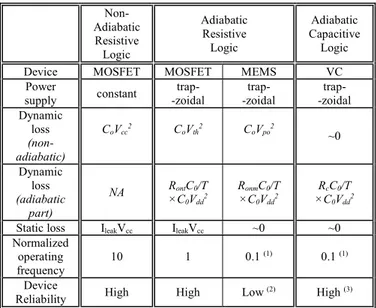
IV. COMPARISONWITHOTHERLOGICSTYLES The key differences with ACL are summarized in Table 1. As the adiabatic logic is based on relay, its static loss is close to zero as it relies on metal-oxide-metal junction. The main benefit of the proposed ACL approach is to avoid the non-adiabatic residue as the capacitor is only modulated instead of switched between on- and off-states in relay counterpart. This contact-less operation also reduces the mechanical contact degradation problem faced in relays. In other part, it reduces the operation frequency as the expected time to modulate the capacitor is significantly longer than the on-to-off switch in CMOS device. Moreover, the smooth transition needed in any adiabatic logic families reduces the frequency. Finally, non-compatible CMOS process is required.
Non-Adiabatic Resistive Logic Adiabatic Resistive Logic Adiabatic Capacitive Logic
Device MOSFET MOSFET MEMS VC
Power supply constant trap- -zoidal trap- -zoidal trap- -zoidal Dynamic loss (non-adiabatic) CoVcc2 CoVth2 CoVpo2 ~0 Dynamic loss (adiabatic part) NA RontC0/T ×C0Vdd2 RonmC0/T ×C0Vdd2 RcC0/T ×C0Vdd2
Static loss IleakVcc IleakVcc ~0 ~0
Normalized operating frequency
10 1 0.1 (1) 0.1 (1)
Device
Reliability High High Low (2) High (3) Table 1: Logic comparison at a glance
Vpo release voltage of relay, Ront and Ronm and are on-state resistances for
transistors and MEMs, respectively, Rc is the interconnect resistance in a
capacitive gate, (1) mechanical time constant is larger than the electrical one, (2) mainly due to the contact, (3) expected as it is a contact-less operation.
V. CONCLUSION
Based on variable capacitor technology it is possible to implement adiabatic capacitive logic (ACL) which is an innovative approach leading to ultra-low inherent static or dynamic energy dissipation hence reducing the power consumption of the existing CMOS digital core by a several decades. ACL is based on two main principles: adiabatic energy transfer and metal-to-metal junctions without physical contact, thus improving the reliability compared to logic based on MEMS relays. This proposal therefore offers new means for near-zero power consumption logic.
REFERENCES
[1] P. Teichmann, “Adiabatic Logic: Future Trend and System Level Perspective,” Springer, Berlin, Germany, 2012.
[2] G. Snider et al., “Minimum energy for computation, theory vs. experiment,” IEEE Conf. Nanotechnology, pp. 478–481, Aug. 2011
[3] M. Spencer et al.: ‘"Demonstration of Integrated Micro-Electro-Mechanical Relay Circuits for VLSI Applications,” IEEE Journal of solid state circuits, vol. 4, Issue 1, pp. 308–320, 2011.
[4] S. Houri et al., “Limits of CMOS Technology and Interest of NEMS, Relays for Adiabatic Logic Applications,” IEEE Trans Circuit and System part 1, 62, pp. 1546–1554, 2015.
[5] Lee J.O. et al., “A sub-1-volt nanoelectromechanical switching device,” Nature Nanotechnology,” vol. 8, pp. 36–40, 2013.
[6] O. Loh and H. D. Espinosa, “Nanoelectromechanical contact switches,” Nature Nanotechnology, vol. 7, No. 5, pp. 283-295, 2012.
[7] C. Pawashe, K. Lin, K.J. Kuhn, “Scaling limits of electrostatic nanorelays,” IEEE Trans. Electron Devices, vol. 60, pp. 2936–2942, 2013. [8] J.G. Koller, W.C. Athas, “Adiabatic switching, low energey computing, and the physics of storing and erasing information”, Proceedings Workshop on Physics and Computation, pp. 267-270, 1992.
[9] C.H. Bennett, “Logical reversibility of computation”, IBM Journal of Research and Development, vol. 17, pp. 525-532, 1973.