Digital-pixel focal plane array development
The MIT Faculty has made this article openly available.
Please share
how this access benefits you. Your story matters.
Citation
Brown, Matthew G. et al. “Digital-pixel focal plane array
development.” Quantum Sensing and Nanophotonic Devices VII. Ed.
Manijeh Razeghi, Rengarajan Sudharsanan, & Gail J. Brown. San
Francisco, California, USA: SPIE, 2010. 76082H-10. ©2010
SPIE--The International Society for Optical Engineering.
As Published
http://dx.doi.org/10.1117/12.838314
Publisher
Society of Photo-optical Instrumentation Engineers
Version
Final published version
Citable link
http://hdl.handle.net/1721.1/58475
Terms of Use
Article is made available in accordance with the publisher's
policy and may be subject to US copyright law. Please refer to the
publisher's site for terms of use.
Digital-pixel Focal Plane Array Development
Matthew G. Brown*, Justin Baker, Curtis Colonero, Joe Costa, Tom Gardner, Mike Kelly, Ken
Schultz, Brian Tyrrell, Jim Wey
MIT Lincoln Laboratory, 244 Wood Street, Lexington, MA 02420
ABSTRACT
Since 2006, MIT Lincoln Laboratory has been developing Digital-pixel Focal Plane Array (DFPA) readout integrated circuits (ROICs). To date, four 256 × 256 30 μm pitch DFPA designs with in-pixel analog to digital conversion have been fabricated using IBM 90 nm CMOS processes. The DFPA ROICs are compatible with a wide range of detector materials and cutoff wavelengths; HgCdTe, QWIP, and InGaAs photo-detectors with cutoff wavelengths ranging from 1.6 to 14.5 μm have been hybridized to the same digital-pixel readout. The digital-pixel readout architecture offers high dynamic range, A/C or D/C coupled integration, and on-chip image processing with low power orthogonal transfer operations. The newest ROIC designs support two-color operation with a single Indium bump connection. Development and characterization of the two-color DFPA designs is presented along with applications for this new digital readout technology.
Keywords: Infrared, Focal Plane Array, ROIC, CMOS, Imaging
1. INTRODUCTION
The digital-pixel ROIC is a novel design concept for infrared FPA readout. The first single color ROIC was produced in 20061. In 2007, a second single color design was fabricated using lessons learned from the 2006 design and
characterization2,3. The 2006 and 2007 ROICs are 256 × 256 single color readouts compatible with 30 μm pitch p-on-n
diode arrays. Design details and characterization data are available in references 1, 2, 3, and 4. In 2008, two new designs with two-color capability were fabricated. The 2008A design used the standard IBM 9SF process, and the 2008B ROIC used the low leakage 9LP process in an attempt to reduce static power dissipation. Design specifications for all 4 designs are given in Table 1. The two-color architecture uses a single bump connection and is compatible with stacked two-color diode arrays. The ROIC can also be operated in single color mode with n-on-p or p-on-n photodiodes. The digital-pixel architecture combined with orthogonal image transfer and bidirectional counting capability allows on-chip processing for non-uniformity correction, TDI, and image filtering. The benefits of these techniques for sensor operability and noise performance are discussed below.
2. DFPA ARCHITECTURE
The heart of the DFPA digital-pixel is a low power current controlled oscillator used to perform in pixel analog-to-digital conversion (ADC). Input photo-current is integrated onto a small parasitic gate capacitance (approximately 1.5 fF) until a threshold voltage of a comparator is reached. The frequency of the output pulses from the comparator is proportional to the input photocurrent. The pulses generated by the comparator increment a ripple counter in the pixel unit cell and provide feedback to reset the integration node. Bidirectional counting is implemented with a one’s complement operation following integration.
*[email protected]; phone 781-981-1383
This work was sponsored by the United States Government under Air Force contract FA8721-05-C-0002. Opinions, interpretations, conclusions, and recommendations are those of the author and not necessarily endorsed by the United States Government
Invited Paper
Quantum Sensing and Nanophotonic Devices VII, edited by Manijeh Razeghi, Rengarajan Sudharsanan, Gail J. Brown, Proc. of SPIE Vol. 7608, 76082H · © 2010 SPIE · CCC code: 0277-786X/10/$18 · doi: 10.1117/12.838314
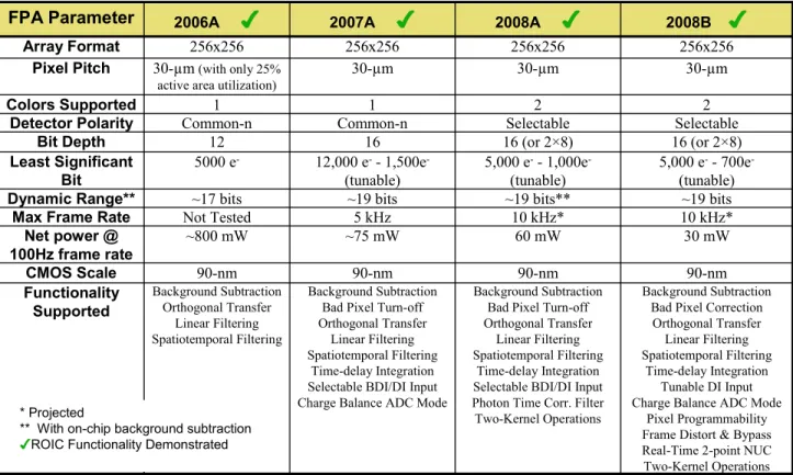
Table 1. Specification for all DFPA ROICs fabricated to date.
FPA Parameter 2006A
✔
2007A✔
2008A✔
2008B✔
Array Format 256x256 256x256 256x256 256x256
Pixel Pitch 30-µm (with only 25%
active area utilization) 30-µm 30-µm 30-µm
Colors Supported 1 1 2 2
Detector Polarity Common-n Common-n Selectable Selectable
Bit Depth 12 16 16 (or 2×8) 16 (or 2×8)
Least Significant Bit 5000 e- 12,000 e-- 1,500e -(tunable) 5,000 e-- 1,000e -(tunable) 5,000 e-- 700e -(tunable)
Dynamic Range** ~17 bits ~19 bits ~19 bits** ~19 bits
Max Frame Rate Not Tested 5 kHz 10 kHz* 10 kHz*
Net power @ 100Hz frame rate ~800 mW ~75 mW 60 mW 30 mW CMOS Scale 90-nm 90-nm 90-nm 90-nm Functionality Supported Background Subtraction Orthogonal Transfer Linear Filtering Spatiotemporal Filtering Background Subtraction Bad Pixel Turn-off Orthogonal Transfer
Linear Filtering Spatiotemporal Filtering
Time-delay Integration Selectable BDI/DI Input Charge Balance ADC Mode
Background Subtraction Bad Pixel Turn-off Orthogonal Transfer
Linear Filtering Spatiotemporal Filtering
Time-delay Integration Selectable BDI/DI Input Photon Time Corr. Filter Two-Kernel Operations
Background Subtraction Bad Pixel Correction Orthogonal Transfer
Linear Filtering Spatiotemporal Filtering
Time-delay Integration Tunable DI Input Charge Balance ADC Mode
Pixel Programmability Frame Distort & Bypass Real-Time 2-point NUC Two-Kernel Operations
FPA Parameter 2006A
✔
2007A✔
2008A✔
2008B✔
Array Format 256x256 256x256 256x256 256x256
Pixel Pitch 30-µm (with only 25%
active area utilization) 30-µm 30-µm 30-µm
Colors Supported 1 1 2 2
Detector Polarity Common-n Common-n Selectable Selectable
Bit Depth 12 16 16 (or 2×8) 16 (or 2×8)
Least Significant Bit 5000 e- 12,000 e-- 1,500e -(tunable) 5,000 e-- 1,000e -(tunable) 5,000 e-- 700e -(tunable)
Dynamic Range** ~17 bits ~19 bits ~19 bits** ~19 bits
Max Frame Rate Not Tested 5 kHz 10 kHz* 10 kHz*
Net power @ 100Hz frame rate ~800 mW ~75 mW 60 mW 30 mW CMOS Scale 90-nm 90-nm 90-nm 90-nm Functionality Supported Background Subtraction Orthogonal Transfer Linear Filtering Spatiotemporal Filtering Background Subtraction Bad Pixel Turn-off Orthogonal Transfer
Linear Filtering Spatiotemporal Filtering
Time-delay Integration Selectable BDI/DI Input Charge Balance ADC Mode
Background Subtraction Bad Pixel Turn-off Orthogonal Transfer
Linear Filtering Spatiotemporal Filtering
Time-delay Integration Selectable BDI/DI Input Photon Time Corr. Filter Two-Kernel Operations
Background Subtraction Bad Pixel Correction Orthogonal Transfer
Linear Filtering Spatiotemporal Filtering
Time-delay Integration Tunable DI Input Charge Balance ADC Mode
Pixel Programmability Frame Distort & Bypass Real-Time 2-point NUC Two-Kernel Operations * Projected
** With on-chip background subtraction
✔ROIC Functionality Demonstrated
The 2008A ROIC uses a reset-to-voltage mode where the reset voltage can be varied to change the amount of charge needed to exceed the comparator threshold. Typically the reset voltage is 100 to 500 mV below (above) the comparator threshold for p-on-n (n-on-p) detectors. For an integration capacitance of 1.5 fF, yields an LSB size of 1000 to 5000 e-. In the 2008B design a charge subtract mode is available in addition to the reset to voltage mode. The charge subtract mode offers two advantages: smaller LSB size and in-pixel LSB tunability. A simple schematic of the digital-pixel is shown in Figure 1. The schematic shows the 2008B design with the charge subtract reset mode. Each pixel has a 12 bit SRAM that allows the user to select the size of the charge subtract packet as well as adjust the pixel bias as set the operating mode. The LSB variation and advantages of LSB tunability for on-chip gain compensation are discussed in Section 3.4.
The DFPA in-pixel ADC design has a number of key differences compared to analog arrays. In the DFPA pixel design, the integration capacitor sets the LSB size and the number of bits in the counter sets the MSB; in analog ROICs the integration capacitor sets the MSB size and the external ADC determines the LSB. The size of the analog integration capacitor limits the well capacity and integration time, while the digital-pixel well capacity is determined by the number of bits in the counter. The digital well does not saturate in the traditional sense; the counter simply rolls over and continues to count. By taking a short integration with no rollover one can calculate a per pixel count rate and correct for counter rollover at long integration times. Using this technique effective well capacities up to 1010 electrons have been demonstrated. Using the bidirectional counting ability effective well capacities of 1011 electrons have been achieved.
This far exceeds the state of the art in analog ROIC performance.
For high flux applications, analog ROICs attempt to maximize the well capacity by using a large capacitor and high voltage processes. The small DFPA transistors and digital nature of the pixel architecture allow the use of advanced CMOS processing. The current generation of ROICs uses 90 nm design rules. Test structures have been fabricated at 65 nm and 45 nm design nodes and future ROIC development will use these smaller design rules. The use of aggressively scaled CMOS technology allows for digital processing within the pixel unit cell. The digital portion of the pixel includes
DETECTOR INPUT VGCN VGCP SELCP SELCP Cint CHARGE SUBTRACT GAIN_ADJ[9:0] SIGN_SELECT SELCP LOCAL SRAM SELCP OSCILLATE ENABLE COUNTER OTS AND DSP LOGIC DETECTOR INPUT VGCN VGCP SELCP SELCP Cint CHARGE SUBTRACT GAIN_ADJ[9:0] SIGN_SELECT SELCP LOCAL SRAM SELCP COUNTER OTS AND DSP LOGIC DETECTOR INPUT VGCN VGCP SELCP SELCP Cint CHARGE SUBTRACT GAIN_ADJ[9:0] SIGN_SELECT SELCP LOCAL SRAM SELCP OSCILLATE ENABLE COUNTER OTS AND DSP LOGIC DETECTOR INPUT VGCN VGCP SELCP SELCP Cint CHARGE SUBTRACT GAIN_ADJ[9:0] SIGN_SELECT SELCP LOCAL SRAM SELCP COUNTER OTS AND DSP LOGIC
Figure 1. Simplified schematic of the 2008B 2-color DFPA digital-pixel.
bidirectional counters and orthogonal transfer capability between the pixel counters. This capability provides on-chip processing options not available in traditional analog ROICs. On- chip background subtraction can be performed by counting up and down for equal increments. If the target is dithered at the up/down counting frequency two target images will be formed: a positive image in the target location during the up counting and a negative image in the target location during the down counting. TDI and on-chip image stabilization are accomplished by shifting the digital image within the ROIC as the target scene moves across the FPA. Also, simple linear filters can be implemented using the integration time as the weighting factor and orthogonal transfer to apply the filter in time2,5. The application of the TDI and up/down counting techniques for reducing noise and improving array operability and performance are discussed in the following sections.
3. 2008 DFPA CHARACTERIZATION
All characterization data presented is collected in a Universal Cryogenics closed cycle helium (He) lab dewar. A custom socket and PCB in the dewar provide an electrical interface for power, biases, clocks, and control signals from external power supplies and a Xilinx Virtex 2 FPGA control board. Data are shown for the 2008A design hybridized to 11 μm cutoff HgCdTe and the 2008B design hybridized to a two-color HgCdTe diode array. The application data for TDI and A/C signal detection was collected with a single color HgCdTe 2007 ROIC, but applies equally to both 2008 designs.
3.1 Power Consumption
Typical power consumption for the core in-pixel analog-to-digital conversion and the counter structures is less than 60 mW for a 256 × 256 array using the standard 9SF process. The power is dominated by static leakage. The low leakage
9LP process dissipates only 30 mW for 100 Hz operation at 68 K and a per pixel photocurrent of 1 to 2 nA. The dynamic power consumption in the DFPA ROIC is dominated by the ripple counter operation and the count rate. Dynamic power scales with the incident flux and count rate. For high background applications, the LSB size can be increased to reduce the count rate and power consumption at the expense of higher digitization noise. This is just one of the advantages offered by the flexibility of the digital-pixel ROIC.
3.2 Two-color Operation
The 2008 ROIC designs are the first DFPAs to support two-color operation. First light images for a two-color HgCdTe diode array with a cutoff wavelength of 9 μm in the short band and 11 μm in the long band are shown in Figure 2. The color is switched by flipping a single control line and changing to detector common bias.
Figure 2. First light images taken with the 2008B ROIC in two long wave infrared bands: 9 micron cutoff (left pane) and 11 micron cutoff (right pane).
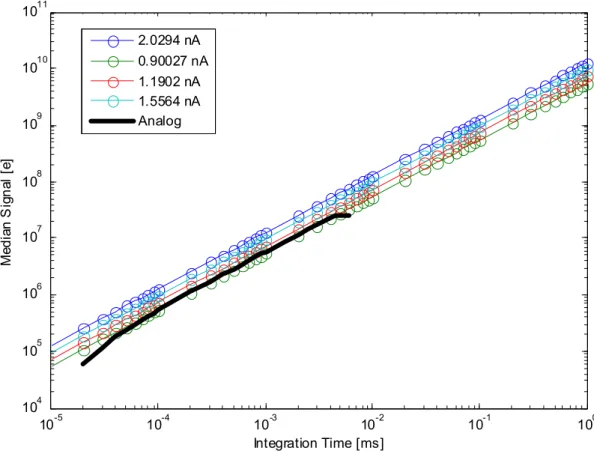
3.3 DFPA Linearity
The current to frequency converter at the heart of the DFPA pixel is extremely linear over the entire dynamic range of the counter. The pulse rate from the converter is directly proportional to the photo-current at fixed flux. The DFPA linearity over 5 orders of magnitude in signal level is shown in Figure 3. Note that the pixel counters roll over after approximately 20 ms. With the digital-pixel architecture we are able to correct for counter rollover using an exposure with a short integration time. The short exposure is used to predict the number of counter rollovers for long integration times. When the correction is applied data remain linear up to an effective well capacity of more than 1010 e-. This
allows integration times of 1 second or more for a long wave HgCdTe detector operating at 77 K. A typical analog ROIC saturates at a well capacity of 10 to 40 Me- after an integration time of only 5 ms. For the digital concept, noise and number of bits are the ultimate limit in well capacity. Utilizing the DFPA bidirectional counting capability the effective well capacity can be extended beyond the 1011 e-. The up/down counting capability is discussed in Section 3.5.
The response of the DFPA pixels has a small non-linearity as the source flux is increased. Each time the current to frequency converter triggers the integrating capacitor must be reset. The reset time for the integrating capacitor affects the pixel linearity as a function of count rate (source flux). The non-linearity is modeled as a constant reset time for the integrating capacitor added to the count rate. This effect is only important when viewing scenes with very large flux dynamic range and can be corrected using laboratory response measurements at the appropriate flux levels.
10-5 10-4 10-3 10-2 10-1 100 104 105 106 107 108 109 1010 1011 Integration Time [ms] M ed ian S ign al [ e] 2.0294 nA 0.90027 nA 1.1902 nA 1.5564 nA Analog
Figure 3. DFPA well capacity and linearity with integration time.
3.4 Spatial Variation and Operability
For the DFPA, the LSB size is set by the node capacitance and the comparator voltage. The node capacitance is due to parasitic gate capacitance and is minimized in the design process to provide a small LSB. The reset voltage is used to vary the LSB size from a maximum of approximately 5000 e-/DN to a minimum of 700 e-/DN in the 2008 ROICs. The integration capacitance is 1.0 to 1.5fF and the voltage swing from reset to the comparator threshold is varied from 100 to 500 mV. The variation in LSB size across the array is due to small differences in capacitance for each pixel’s comparator. Spatial sensitivity variations in the diode array cannot be decoupled from the LSB variation in the array characterization process. The combined LSB and diode sensitivity variations lead to a responsivity variation across the array. A representative response map and histogram are shown in Figure 4. These data are collected viewing a 25 C flood blackbody through an f/3 cold stop with an integration time of 256 μs.
The 2008B ROIC unit cell contains a 12 bit SRAM for LSB tunability. This is implemented with a charge subtract reset mode. The size of the charge packet can be varied to 32 different levels using 5 of the SRAM bits. This mode has not yet been characterized and will be discussed in a future publication.
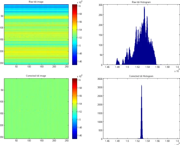
Figure 4. Map and histogram of DFPA spatial sensitivity variation. Data include both LSB variation and diode array spatial sensitivity variations. σ/mean = 7.43%.
Figure 5. Image and histogram of DFPA raw TDI output (top row) and TDI with a simple row by row gain correction applied (bottom row). The spatial variation is reduced from 7.43% without TDI (Figure 4) to 0.055% in the corrected TDI image.
A second option for reducing the spatial variability in the output frame is to employ a TDI technique. When using TDI the images are scanned across the FPA and the pixel values are synchronously shifted on the FPA to provide coherent integration of the scene. For a 1D scan, the signal is integrated over 256 pixels in the FPA. The result is to reduce the effective LSB distribution for the output image by averaging over the different LSB sizes. Figure 5 shows the LSB distribution for the array after a 1D scan with 256 stages of TDI. The variation in the LSB size is reduced to 1% in the raw TDI frame, but a row structure appears due to the distribution of under and over responsive pixels in the array. After applying a simple row by row gain correction the total variation is reduced to only 0.055% (bottom of Figure 5).
A prototype 1D TDI sensor has been developed to demonstrate the capability of the digital-pixel ROIC in a TDI sensor. A sample image is shown in Figure 6. These data represent at 9 x 150 degree TDI scan with a refresh rate of 66 Hz4.
256 stages of TDI with a dwell time or 1μs per stage provide a NEDT of approximately 60 mK. Based on this concept a 2-D scanning sensor has been built and integrated with an airborne platform. Results from this sensor will be presented in a future publication.
The same averaging affect shown in the TDI data can be achieved by dithering the target in the sensor field of view during the integration period. Sensors that require high rate inertial measurement units (IMUs) and gimbals to stabilize a scene on a conventional analog FPA can be replaced by a DFPA which stabilizes the image on the chip with the added benefit of averaging the target signal over many pixels to reduce spatial variation in the focal plane. This technique can be applied to airborne and space-based surveillance platforms as well as infrared missile seekers.
3.5 DFPA Noise
The DFPA noise power spectral density is shown in Figure 7. The 2 plots show the noise for a representative pixel based on the raw pixel output (left figure), and after correcting the output for global variations in FPA output due to the He compressor on the lab test dewar. The frequency spike near 3 Hz is due to the closed cycle He refrigerator system. The large dynamic range of the DFPA allows for integration times of 1 second or more, which samples low frequencies when making laboratory measurements of detector noise. For a typical noise measurement we collect 128 frames of data
~ 1km FOV = 150-deg
Figure 6. (A) One frame from 150-deg x 9-deg LWIR 66 Hz video taken with a brassborad TDI camera. (B) Google maps overhead image showing location from which the image was taken and the field of regard. (C) A zoomed window (indicated in A) of a 256 x 256 section of the raw image. This window corresponds to the staring format of the DFPA used to collect the imagery.
A.
to compute the temporal standard deviation of each pixel in the array. This probes frequencies as low as 0.01 Hz where 1/f noise can make a significant contribution to the data.
Figure 7. DFPA Power Spectral Density. The left figure shows raw DFPA data and the right figure shows the data after correcting for the effects of the He refrigerator.
The DFPA offers a number of options to combat the low frequency noise at long integrations. For shuttered operation, bidirectional counting can be used to integrate up when the shutter is open, and down when the shutter is closed. This process can be repeated for many cycles before reading out, leading to a very long total exposure but significantly reduced 1/f noise. The advantage offered by the digital ROIC is that a large number of up and down integrations can be performed within a single readout. For example, to achieve a total integration of 500 ms with a signal chopped at 1000 Hz an analog array would have to read out at 2 KHz, collect 1000 0.5 ms frames with the chopper open and 1000 0.5 ms frames with the chopper closed, then buffer and average the frames in an off chip signal processor. The output of the process is a 1 Hz background subtracted image with an effective integration time of 500 ms. The digital-pixel ROIC completes all of the averaging on the chip and outputs a 1 Hz, background subtracted signal with minimal power dissipation and no off chip processing.
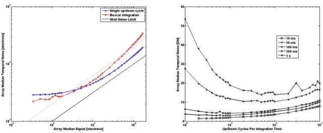
Figure 8 shows the noise performance for one of the 2008B ROICs along with measurements taken at a number of different up/down counting frequencies. A comprehensive DFPA noise model has been developed and is presented in reference 5. The 3 main contributors to the DFPA noise are read noise, shot noise, and 1/f noise. Johnson noise, KTC noise from resetting the integration transistor, and other noise sources are minimal in the current architecture. At short integration times, the read noise dominates. This is evident in the low signal data in the left panel of Figure 8. The read noise is due to the unknown amount of charge on the integration capacitor at the start and end of integration. Its magnitude is sqrt(2/12)*LSB. Reducing the LSB reduces the read noise component. The magnitude can be reduced to sqrt(1/12)*LSB by implementing a global reset before the start of integration. This has been demonstrated in the 2007 design.
For well capacities of 5 to 50 Me-, shot noise is the dominant noise component. This is consistent with the performance of LWIR analog arrays with well capacities of 10 to 40 Me-. The digital-pixel ROIC noise performance nearly matches analog ROICs in this region. For well capacities above 50 Me-, 1/f noise dominates the measurement. The data shown use a constant flux source and change integration time to vary the signal level. Integration times up to 1 second are used. The noise measurement consists of taking the standard deviation for each pixel in the array through a stack of 128 frames. This leads to very long measurement times and noise bandwidths including frequencies down to 0.01 Hz.
Figure 8. DFPA noise for a standard ‘boxcar’ integration and an on-chip ‘CDS’ integration (left). DFPA noise (in DN) with up/down counting implemented (right).
The right panel of Figure 8 shows the noise performance when implementing on-chip up/down counting. Each curve represents a fixed total integration time. The x-axis shows the number of up/down counting cycles. The data on the left side of the plot are 1/f noise limited, and the data on the right are read noise limited. The ideal frequency and number of up/down cycles is application dependent.
The DFPA on-chip up/down counting capability has been demonstrated for applications requiring measurement of a small A/C signal in the presence of a large D/C background. A 1 KHz A/C signal is generated with a chopped blackbody source and imaged onto the FPA in the presence of a high flux D/C background signal. The D/C background is 4.5 orders of magnitude greater than the A/C signal component. The resulting signal shown in Figure 9 is detected with an SNR of approximately 10 after averaging ten, 100 ms on-chip integrations with the DFPA up/down counting synchronized to the chopper wheel. The effective integrated signal is over 1011 electrons per frame. On-chip up/down counting can also be used for synchronous detection of laser pulses in the presence of high background clutter. See reference 4 for more details.
A/C Signal
D/C Background
D/C background 4.5-5 orders-of-magnitude greater than A/C signal
A/C Signal
D/C Background D/C Background
D/C background 4.5-5 orders-of-magnitude greater than A/C signal
Figure 9. Laboratory demonstration of detection of an A/C signal in the presence of a large D/C background. A/C signal intensity was 4.5 orders-of-magnitude less than the D/C background.
4. SUMMARY
MIT Lincoln Laboratory has fabricated a digital-pixel ROIC with on-chip processing capability for infrared focal plane arrays. In 2008, two two-color ROICs were produced. The two-color ROIC have been operated with stacked two-color HgCdTe diode arrays. Signal integration in the DFPA ROIC uses a digital well that does not saturate in the manner of a
traditional analog FPA. With simple processing effective well capacities of 1010 e- or more are possible. The ability to
perform orthogonal image transfer has been demonstrated in a 1D TDI sensor with a large number of integration stages. This functionality can also be used to implement on-chip image stabilization and non-uniformity correction. Up/down counting in the pixel unit cell allows for on-chip background correction, frame averaging, and synchronous detection of laser pulses and A/C signals. These unique capabilities make the digital-pixel focal plane a valuable tool for a number of applications in infrared imaging and surveillance.
5. ACKNOWLEDGEMENTS
The authors would like to thank MDA/DV for sponsoring the TAPO runs to fabricate the DFPA ROICs and funding the 2008A ROIC, and DDR&E for sponsoring the 2008B ROIC design.
REFERENCES
[1] M. Kelly, R. Berger, C. Colonero, M. Gregg, J. Model, D. Mooney, E. Ringdahl, “Design and testing of an all-digital readout integrated circuit for infrared focal plane arrays.” Proceedings of SPIE, Volume 5902, 2005, pp. 105-115.
[2] M. Kelly, C. Colonero, B. Tyrrell, and K. Schultz. “The Digital Focal Plane Array (DFPA) Architecture for Data Processing “On-Chip”. MSS Detectors. February 2007.
[3] B. Tyrrell, R. Berger, C. Colonero, J. Costa, M. Kelly, E. Ringdahl, K. Schultz, J. Wey. “Design Approaches for Digitally Dominated Active Pixel Sensors: Leveraging Moore’s Law Scaling in Focal Plane Readout Design.” Proceedings of SPIE, Volume 6900, 2008.
[4] M. Kelly, D. Klick, M. Beattie, C. Colonero, B. Tyrrell, D. Hearn, D. Johnson, K. Schultz, and A. DeCew, “A DFPA-Based LWIR Sensor for Night-time Wide-Area Persistent Surveillance.” MSS Passive Sensors, February 2008.
[5] B. Tyrrell et al. “Time Delay Integration and In-Pixel Spatiotemporal Filtering Using a Nanoscale Digital CMOS Focal Plane Readout.” IEEE Transactions on electron Devices, Vol. 56, No. 11, November 2009.