https://doi.org/10.1149/osf.io/68puc
READ THESE TERMS AND CONDITIONS CAREFULLY BEFORE USING THIS WEBSITE.
https://nrc-publications.canada.ca/eng/copyright
Vous avez des questions? Nous pouvons vous aider. Pour communiquer directement avec un auteur, consultez la
première page de la revue dans laquelle son article a été publié afin de trouver ses coordonnées. Si vous n’arrivez pas à les repérer, communiquez avec nous à PublicationsArchive-ArchivesPublications@nrc-cnrc.gc.ca.
Questions? Contact the NRC Publications Archive team at
PublicationsArchive-ArchivesPublications@nrc-cnrc.gc.ca. If you wish to email the authors directly, please see the first page of the publication for their contact information.
NRC Publications Archive
Archives des publications du CNRC
This publication could be one of several versions: author’s original, accepted manuscript or the publisher’s version. / La version de cette publication peut être l’une des suivantes : la version prépublication de l’auteur, la version acceptée du manuscrit ou la version de l’éditeur.
For the publisher’s version, please access the DOI link below./ Pour consulter la version de l’éditeur, utilisez le lien DOI ci-dessous.
Access and use of this website and the material on it are subject to the Terms and Conditions set forth at
Determining strain, chemical composition, and thermal properties of Si/SiGe nanostructures via raman scattering spectroscopy
Tsybeskov, L.; Mala, S. A.; Wang, X.; Baribeau, J.-M.; Wu, X.; Lockwood, D. J.
https://publications-cnrc.canada.ca/fra/droits
L’accès à ce site Web et l’utilisation de son contenu sont assujettis aux conditions présentées dans le site LISEZ CES CONDITIONS ATTENTIVEMENT AVANT D’UTILISER CE SITE WEB.
NRC Publications Record / Notice d'Archives des publications de CNRC: https://nrc-publications.canada.ca/eng/view/object/?id=76071b9f-bc78-477a-9036-2852a33a9f28 https://publications-cnrc.canada.ca/fra/voir/objet/?id=76071b9f-bc78-477a-9036-2852a33a9f28
Determining Strain, Chemical Composition, and Thermal Properties of Si/SiGe Nanostructures via Raman Scattering Spectroscopy
L. Tsybeskov,a S. A. Mala,a X. Wang,a J.-M. Baribeau,b X. Wu,b and D. J. Lockwoodb
a Department of Electrical and Computer Engineering, New Jersey Institute of
Technology, Newark, NJ 07102, USA
b National Research Council, Ottawa, ON KIA 0R6, Canada
Studies by Raman spectroscopy of two kinds of Si/SiGe
nanostructures—quantum dot multilayers and planar
superlattices—reveal a wide variety of spectral features including first- and second-order Raman scattering, polarized Raman scattering, and low-frequency inelastic light scattering associated with folded acoustic phonons. Here we overview how such features can be employed to semi-quantitatively analyze the strain, chemical composition, and thermal conductivity in these industrially important materials that are widely used for producing electronic and optoelectronic devices.
Introduction
Inelastic light (Raman) scattering is an important general characterization technique (1), which, along with x-ray diffraction (2,3), can provide a great deal of information about the structural and, particularly for Raman scattering, the electronic properties of Si/SiGe nanostructures (4–8). Raman scattering from semiconductor nanostructures involves a variety of different phonons that are observed according to strict optical polarization selection rules. Such scattering can also result in additional spectral features at wavenumbers between those of lower-frequency acoustic phonons and higher-frequency optical phonons (9). Similar to what is observed for bulk SiGe alloys, the Raman spectrum of Si/SiGe nanostructures comprises three major bands with a Si-like (Si-Si) peak at ~ 500 cm-1, an alloy-like (Si-Ge) peak at ~ 400 cm-1, a Ge-like (Ge-Ge) peak at ~
300 cm-1 together possibly with a crystalline Si (c-Si) peak at~520 cm-1 depending on the
sample composition , together with weaker Raman features located between the three major peaks (4–8,10,11). These weaker Raman features are attributed to localized vibrational modes (e.g., Si-Si vibrations in the presence of a Ge atom, etc.) and various overtones (9,12). Light scattering observed at low wavenumbers (< 100 cm-1) is usually
associated with various acoustic phonons, and second-order Raman scattering produces multiple overlapping peaks located between 600 and 1200 cm-1 (9). Thus, in Si/SiGe
nanostructures the entire spectral region of 0-1200 cm-1 is covered by multiple Raman
peaks, and the energies and appearances of these peaks display strong dependences on the growth conditions, strain, temperature and chemical composition.
The intensity of a Raman peak is proportional to its Raman cross-section and the scattering volume, which is related to the light penetration depth and hence the optical
absorption coefficient (13). Resonant Raman scattering (RRS) occurs when the excited or scattered light approaches an energy gap in the material and is thus associated with significant changes in the Raman cross section, which are directly related to the joint density of states in the electronic bands of bulk materials or nanostructures (13). While c-Si does not exhibit any resonances within the full visible spectrum, crystalline Ge (c-Ge) has a well-known resonance at ~2.2 eV associated with E1 and E1 + Δ1 electronic
transitions in the L direction of the Brillouin zone (9). Thus, in Si/SiGe nanostructures the intensity of a Raman peak as a function of the incident light energy exhibits a broad peak around 2.2– 2.5 eV (14,15). The optical polarization dependence of the Raman intensity of any given excitation is symmetry determined and is defined by its Raman scattering tensor (13). In Si/SiGe nanostructures, an analysis of the polarization dependence of the light scattering has been used to detect various imperfections, including inhomogeneous strain, in epitaxially grown samples (16–18).
This overview of the use of Raman spectroscopy for characterizing Si/SiGe nanostructures covers the following topics: what inelastic light scattering reveals in various such nanostructures with respect to both acoustic and optical phonons; analysis of strain and composition; evaluation of thermal properties; and the application of polarized Raman scattering in detecting strain.
Introduction Growth and Structural Properties of Si/SiGe Nanostructures for both Superlattices and Cluster Multilayers
Planar Si/Si1-xGex superlattices (SLs) are fashioned from alternating thin layers of Si
and Si1-xGex with x usually less than 0.5 and are commonly prepared by molecular beam
epitaxy (MBE) growth on (001)-oriented Si substrates at a temperature of ~ 500oC (see
Fig. 1 and Ref. 19 for example). This relatively low growth temperature is chosen to produce dislocation-free pseudomorphic growth and to help prevent Si/SiGe intermixing and thereby curtail the interface roughness. However, as can be seen from Fig. 1(b), the Ge composition in the alloy layer can vary across the start and end of the layer. For a SiGe layer with thickness below a critical value, the in-plane lattice mismatch between Si and SiGe is expected to be accommodated by a homogeneous tetragonal compression, which results in an extension of the lattice constant in the growth direction. These compressed SiGe layers are combined with the alternating Si layers, which may also be slightly strained, to form Si/Si1-xGex/Si… strained-layered SLs that are usually capped
with a Si layer.
Cluster multilayers (CM) of Si/Si1-xGex are grown using Si1-xGex layer thicknesses
approaching, or above, the critical value, and hence the epitaxial growth of SiGe on Si requires relief of the elastic energy in the strained SiGe film (20–23). At high growth temperatures, the adatom diffusion and elastic deformation trigger a transition from two-dimensional (2D) to three-two-dimensional (3D) growth modes. This 3D growth mechanism is known as Stranski-Krastanov (S-K) growth, and it is typically observed at MBE growth temperatures of 550-650oC. As can be seen in Fig. 2(a), the strain involved during
growth of the first two or three alloy layers produce self-organized dome-like structures (23) that stack up nicely throughout the remaining layers (see Fig. 2(b) and (c)). In the case of chemical-vapor-deposition based S-K growth, GeH4 diluted in H2 is used for
providing the Ge atoms and spontaneous Si-Ge intermixing occurs due to thermal and strain-induced diffusion. In the S-K growth mode, most of the SiGe clusters (or islands)
have a pyramid/dome-like (uncapped) or pancake-like (Si capped) shapes with the Ge concentration gradually increasing toward the cluster core (20–23).
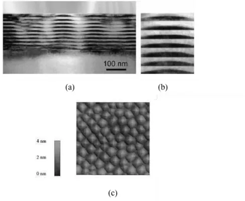
(a) (b)
Figure 1. (a) Cross-sectional transmission electron micrograph (TEM) image of a 500oC
MBE grown planar Si/Si0.65Ge0.35 superlattice and (b) an energy dispersive x-ray (EDX)
scan of the structure revealing the atomic composition of the top-most layers.
Figure 2. (a) Cross-sectional TEM image of a 650oC MBE grown Si/SiGe cluster
multilayer nanostructure, (b) an enlarged TEM image of a section of the structure showing the strain-driven stacked growth of the SiGe clusters, and (c) an atomic force microscopy image of the uncapped alloy sample surface.
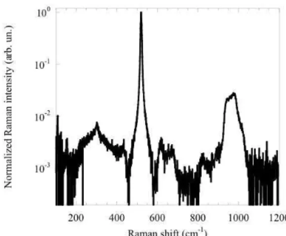
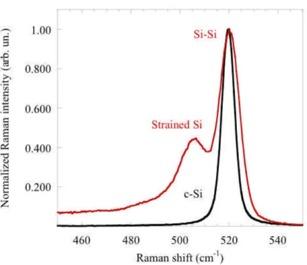
First-Order and Low-Wavenumber Raman Scattering in Si/SiGe Nanostructures The Raman spectrum of bulk Si, as shown in Fig. 3, is comprised of a strong first-order peak at 520 cm-1 that is surrounded by a variety of weaker second-order features
that are associated with various combinations of acoustic and optical phonons. A SiGe alloy Raman spectrum is even more complicated, as can be seen in Figs. 4 and 5. Here, in accordance with the expectations mentioned above, three first-order Raman lines are visible. These three lines are usually weaker and wider than that of c-Si and can be asymmetric in shape. Also, the underlying continuum of second-order scattering is modified from that found in Si and is relatively stronger. Such differences need to be kept in mind when interpreting Raman spectra of Si/SiGe nanostructures.
Figure 3. Raman vibrational spectrum of bulk c-Si at room temperature showing a very strong and sharp peak at 520 cm-1 that arises from first-order Raman scattering and
various other weaker and broader features arising from second-order scattering. Note the use of a logarithmic vertical scale.
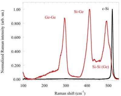
Figure 4. Room-temperature Raman spectrum of a Si/Si1-xGex Si/SiGe cluster multilayer
nanostructure showing major peaks associated with the Si layers at 520 cm-1, and the
strained alloy layers due to Si-Si (at ~500 cm-1), Si-Ge (at ~400 cm-1), and Ge-Ge (at
~300 cm-1) type lattice modes. A normalized Raman spectrum of c-Si is shown for
Figure 5. As for Figure 4, but showing only the Si-type vibrational modes of the Si and SiGe layers.
Figure 6 displays the Raman spectrum of a Si/Si1-xGex SL (see TEM image in Fig. 1)
with the three distinct Raman peaks associated with the Si-Si, Si-Ge and Ge-Ge local bond vibrations. In addition to the major Si-Si Raman peak at 520 cm-1 with a full-width
at half-maximum (FWHM) of 5-6 cm-1, a weaker peak at 505-506 cm-1 is found that is
attributed to a Si-Si vibration in the presence of a nearby Ge atom (8,12,19). In both Si/SiGe SLs and S-K CMs, curve fitting of the spectra indicates that the FWHM of the 505-506 cm-1 peak precisely correlates with the FWHM of the major Raman peak at 520
cm-1 (12). It was concluded that in both Si/SiGe SLs and S-K CMs, the Si layers
separating the SiGe layers are strained and the strain in SL Si layers is more homogeneous compared to that found in CMs (12). Si/Si1-xGex nanostructures with x ≥
0.4 and thicker SiGe layers usually show a main Si-Si type Raman peak at ~ 490 cm-1
(Fig. 7) plus a weaker one at 510 cm-1, which is attributed to a localized Si-Si vibration
mode arising from the presence of Ge (10). However, if the excitation wavelength is long enough so that the exciting light can reach the c–Si substrate, Raman peaks at 520, 508 and 490 cm-1 can all be observed (Fig. 7). Raman spectra associated with Si-Ge and
Ge-Ge vibrations in the SL sample are peaked at 417-418 cm-1 and 298-299 cm-1,
Figure 6. Raman spectrum at room temperature of a Si/Si1-xGex cluster multilayer
nanostructure similar to the one shown in Fig. 2, with x ≈ 0.5, displaying peaks associated with first-order Brillion-zone-center optical phonons in the Si and strained alloy (Si-Si, Si-Ge, and Ge-Ge modes). Notably, a peak due to the influence of a Ge atom on the Si-Si mode [Si-Si (Ge)] is also visible. The Raman spectrum was recorded with 457.9 nm excitation. The Raman spectrum of c-Si is given for comparison purposes.
Figure 7. Room-temperature Raman spectrum of a Si/Si1-xGex cluster multilayer
nanostructure with x≈0.5 exhibiting a Raman peak at ~ 490 cm-1 that is attributed to the
local Si-Si vibration mode in the presence of Ge [Si-Si (Ge)]. Raman peaks are also observed at 508 (Si-Si) and 520 (c-Si) cm-1. The Raman spectrum was recorded with
Figure 8. Room-temperature Raman spectra associated with Si-Ge and Ge-Ge vibrations at 417-418 cm-1 and 298-299 cm-1, respectively, in Si/SiGe Stranski-Krastanov cluster
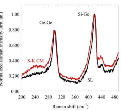
multilayers (S-K CM) and planar superlattices (SL).
In S-K CM samples, the Si-Ge and Ge-Ge peaks are broader by ~3 cm-1 and are
slightly shifted toward lower wavenumbers compared to that in comparable SL samples, as shown in Fig. 8. In addition, the Raman spectra show weaker and broader peaks at ~250 cm-1 attributed to the resonant Ge vibrational mode in the alloy and at 438 cm-1
associated with the local Si vibrational mode in the presence of Si and Ge, respectively (3,24). These peaks are enhanced in S-K CMs compared to SL samples, most likely due to the higher Ge composition. Figure 9(a) presents a summary of the reported dependence of the Raman peak wavenumbers associated with Si-Si, Si-Ge and Ge-Ge vibrations on the composition x in bulk Si1-xGex alloys, where there should be no strain (24). The
results are compared to that in Si/SiGe nanostructures with various degree of strain (Fig. 9(b)), and the following composition dependencies are found (24):
(a) In bulk Si1-xGex alloys, the Si–Si Raman peak wavenumber linearly decreases
with increasing x, as ωSi-Si = 521.2 – 67.91x. In Si/Si1-xGex SL nanostructures, the
dependence is much weaker; ωSi-Si = 519.9 – 29.82x.
(b) In bulk Si1-xGex alloys, the Ge–Ge Raman peak wavenumber linearly increases
with increasing x, ωGe-Ge = 280.8 + 19.37x. In Si/Si1-xGex SL nanostructures, the
dependence is stronger; ωGe-Ge = 282.0 + 33.53x.
(c) In bulk Si1-xGex alloys, the Si–Ge Raman peak wavenumber increases for x < 0.6
and decreases for x > 0.6: ωSi-Ge = 400.0 + 22.07x – 36.14x2 + 83.73x3 – 88.54x4.
However, in Si/Si1-xGex SL nanostructures the dependence can be described as ωSi-Ge =
Figure 9. A summary of previously reported dependencies of the Raman peak wavenumbers associated with Si-Si, Si-Ge and Ge-Ge vibrations on the alloy composition x in (a) bulk Si1-xGex alloys and (b) Si1-xGex planar superlattices (●) and
cluster multilayers (□) with various degrees of strain. See Reference 24 for further details. The results presented here indicate that apart from just the average composition x of Si/Si1-xGex nanostructures other factors such as layer thicknesses, Si-Ge inter-diffusion,
SiGe island sizes and shapes, and local strain should all be to be taken into account in analyzing the Ge concentration dependencies of the Raman peak wavenumbers and intensities. The most common explanation for the observed behavior is that an accumulation of Ge in the middle of planar layers and within the SiGe island core is responsible for a non-uniform composition and strain distribution (23). Possible detailed mechanisms include: the out diffusion of Ge and formation of compressed Si rich alloy regions in the valleys of the Si1-xGex island multilayers; a strong diffusion coefficient
dependence on the local Ge concentration in the film; and the tensile strain in the Si spacer layer placed on top of the SiGe islands (3,24).
In Si/SiGe periodic nanostructures, multiple Raman peaks at low wavenumbers (< 100 cm-1) observed in the backscattering geometry are associated with folding of
longitudinal acoustic (FLA) phonons due to the growth introduced new periodicity PSL
and the formation of the Brillouin mini-zone. A commonly used method for the calculation of phonon dispersion curves is to use the elastic continuum model by Rytov (25). A condition of this model is that the wavelength of the sound wave should be much larger than the layer thickness. The elastic continuum approximation is then valid and the wave equation in each layer can be solved. Figure 10(a) shows the low-frequency Raman spectrum in a Si/SiGe SL (as shown in Fig. 1(a)) with distinct Raman doublets
corresponding to various FLA modes. The inset shows a simplified FLA phonon dispersion diagram based on Rytov’s model. In reality, band gaps appear at the mini-zone center and boundary (Fig. 10(b)) due to the difference in the acoustic impedances of the two component layers of the SL (19). These gaps are barriers to phonon propagation along the SL growth direction for those phonons having the appropriate energies and wave vectors. Thus, these Si/SiGe periodic nanostructures are the first known examples of one-dimensional phononic crystals (19).
Figure 10. (a) Raman spectrum at low wavenumbers of a Si/Si0.65Ge0.35 planar
superlattice at room temperature. The acoustic phonon peaks visible in this spectrum appear in pairs in accordance with their zone folding index m. The inset shows a schematic of the formation of the Brillouin mini-zone and the anticipated peak positions due to Raman interactions with folded longitudinal acoustic (FLA) phonons for this sample. (b) The measured points and dispersion relation (dashed lines) of the FLA phonons near the mini-zone-edge phononic band gap arising from the difference in the acoustic impedances of the two component layers of the Si/Si0.5Ge0.5 superlattice. For
further details, see Reference 19.
Second-Order Raman Scattering in Si/SiGe Nanostructures
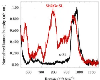
In Si/SiGe nanostructures, several Raman peaks associated with second-order light scattering are observed between 550 and 1100 cm-1 (Fig. 11). The two-transverse optical
(2TO) Si phonon overtone features are related to scattering from the Brillouin zone critical points at W and L, and occur at 940 and 975 cm-1, respectively (26,27). The 2TO
Raman signal shown in Fig. 11 is actually comprised of three peaks: the major Raman peak associated with scattering from the 2TO(L) phonon combination, the 2TO(W) Raman peak, and a weak shoulder associated with the 2TO(Γ) phonon overtone. In most of the Si/SiGe nanostructures we investigated, we also found prominent Raman features associated with second order Si-Ge vibrations around 800 cm-1 and second order Ge-Ge
vibrations at ~ 600 cm-1. Other weaker Raman features at ~680 cm-1 and in the range of
840-900 cm-1 are, most likely, overtones of the first-order Ge-Ge (in the presence of Si)
and local Si-Si (in the presence of Ge) modes (27).
Figure 11. Spectral details of the second-order Raman scattering in c-Si and a Si/Si1-xGex superlattice (SL) with x=0.4 involving optical phonons at wavenumbers in the
range 550–1150 cm-1.
Strain and Chemical Composition in Si/Si1-xGex Nanostructures
In Si/Si1-xGex nanostructures, correlations between the Si-Si, Si-Ge, and Ge-Ge
Raman peak wavenumbers, Ge content x, and strain ε have been discussed extensively (3,24,28). The relative numbers of chemical bonds comprising the Si-Si, Si-Ge, and Ge-Ge phonon modes are estimated to be varying with x as (1-x)2, 2x(1-x), and x2,
respectively. Since the Raman intensity is proportional to the scattering volume, the ratio of the integrated Raman peak intensities related to the relative number of chemical bonds of the corresponding phonon modes can be described as follows:
IGe-Ge/ISi-Ge = Bx/2(1 – x) [1]
and
ISi-Si/ISi-Ge = A(1 –x)/2x , [2]
where coefficients A and B are related to the frequencies of the optical modes in the SiGe alloy. It was found experimentally that B = 3.2 and A = 1.85 for 457.9 nm excitation (29). This so-called intensity method for determining the value of x is independent of strain in the alloy layer and depends on the integrated intensity of the Raman signal associated with the phonon bands. In the Raman peak position (or wavenumber) method, a set of three equations is derived, where the peak positions of the three major vibrational modes in Si/Si1-xGex nanostructures are described as a function of x and ε. The wavenumber of
ω = ω0 + bε, [3]
where ω0 is the x dependent phonon frequency of the unstrained SiGe alloy and b is the
strain-shift coefficient. In the case of a strained Si1-xGex (0 < x < 0.5) layer, the
wavenumbers of the three different phonon modes are (28,29):
ωSi-Si = 520.2 – 70.5x – 830ε, [4]
ωSi-Ge = 400.5 + 16.3x – 575ε, [5]
and
ωGe-Ge = 282.5 + 16x – 384ε. [6]
The average values of x and ε in the alloy layer are
x = [(ωSi-Ge – 400) – 0.7(ωSi-Si – 520)]/65 [7]
and
ε = [(400 – ωSi-Ge) + 0.23(520 – ωSi-Si)]/767. [8]
On considering previously published data (3,12,24), we find a reasonably good agreement between results obtained by both methods.
Raman Studies of Thermal Conductivity and Heat Dissipation in Si/Si1-xGex Nanostructures
Typically, Raman scattering measurements are performed using an intense laser beam. While c-Si and c-Ge have a high thermal conductivity (κ ≈ 100 Wm-1 K-1), in
compositionally disordered SiGe alloys and Si/SiGe nanostructures κ ≤ 10 W m-1 K-1 (30).
Thus, a significant temperature increase of a sample might occur during Raman scattering measurements and it will affect the Raman peak position, width, and line shape. Using a model based on the Fourier law of heat conduction, the thermal conductivity can be calculated as
κ = P*(L/A)*(1/ΔT), [9]
where P is the laser power absorbed by a sample with a thickness L in the direction normal to a surface of a cross-sectional area A due to a temperature gradient ΔT. The temperature gradient is established between the highest temperature at the sample surface and the lowest temperature of the c-Si substrate (due to the high c-Si thermal conductivity), and these temperatures can be calculated using the Stokes/anti-Stokes Raman peak intensity ratio IS/IaS for strained Si and Si-Ge phonon modes and the Si-Si
mode at 520 cm-1 (assuming that it is associated with the c-Si substrate). This is because,
to a good approximation, IS/IaS = exp(ћω/kBT), where ћ = h/2π, h is Planck’s constant, kB
is Boltzmann’s constant, and T is the sample temperature, provided that the excitation conditions are the same for both the Stokes and anti-Stokes scattering and there is no Ge
resonance effect (see the Introduction). In measured samples (see, for example, Fig. 12) the calculated thermal conductivity is ~ 12 W cm-1 K-1 for Si/Si/SiGe SLs and is ~ 4 W
cm-1 K-1 in Si/SiGe CMs, respectively. The reason for the lower thermal conductivity
found in Si/SiGe CMs compared to Si/SiGe SLs can be explained by analyzing a comparative volume fraction of SiGe (a lower thermal conductivity material) versus c-Si (a higher thermal conductivity material) and quality of the Si/SiGe heterointerfaces. In Si/SiGe CMs, we typically find that the volume fraction of SiGe is nearly twice that of Si/SiGe SLs, and it has been noted that inelastic scattering of phonons in Si/SiGe nanostructures with a diffuse interface also contributes to the reduction in the thermal conductivity (31). It was also reported that the temperature calculated according to Boltzmann statistics under a non-resonant excitation condition of the Ge-Ge phonon mode is consistently lower than that found for the Si-Ge and Si-Si modes (30). This discrepancy can be explained assuming that at the laser excitation wavelengths used, the Ge-Ge phonon mode has a resonant component, as pointed out in References 12, 32, and 33.
Figure 12. A comparison of the Stokes and anti-Stokes Raman spectrum recorded nominally at room temperature for a Si/SiGe cluster multilayer nanostructure sample. (a) The raw spectrum. (b) The Stokes and anti-Stokes spectra scaled to show the differences in the relative intensities of the main features.
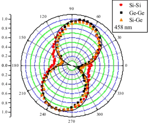
Polarization Dependent Raman Scattering in Si/SiGe Nanostructures
Polarized Raman scattering in the form of polar plots provides information on the Raman scattering intensity as a function of the polarization angle of the scattered light (16–18). The particular shape of the polar plot depends on the symmetry of the vibrational mode being measured and the crystallographic orientation of the sample. Figure 13 displays angular Raman polarization diagrams for three different vibrational modes (Si–Si at 520 cm−1, Si–Ge at 415 cm−1, and Ge–Ge at 298 cm−1) for a Si/SiGe S-K
CM sample (16). The observed angular dependencies of the Ge–Ge and Si–Ge Raman mode intensities are nearly identical to that measured in a (100)-oriented Si single crystal (shown in Fig. 13 by the solid line). However, a quite different behavior is observed in the Raman polarization dependence for the Si-Si Raman mode at 520 cm-1. The observed
deviation is explained by strain-induced partial relaxation of selection rules, mixing of different phonon modes in the nanometer-thick Si layers separating the SiGe cluster layers, and, possibly, from scattering in a thin layer of the c-Si substrate directly under the sample, which can exhibit stress in response to the S-K CM structure above it. The
strong localization of strain observed in the Si layers is consistent with present understanding of the nature of vertical self-ordering produced by strain propagation in Si/SiGe S-K CM nanostructures. Similar measurements performed on Si/SiGe SL samples did not reveal any deviation from the data obtained in (100) c-Si substrates.
Figure 13. Angular Raman polarization diagrams of the Si–Si, Si–Ge, and Ge–Ge vibrational modes for a Si/SiGe Stranski-Krastanov cluster multilayer sample measured at room temperature using laser excitation at 457.9 nm. The Raman polarization diagram of single-crystal (100)Si (solid line) is shown for comparison.
Conclusions
In conclusion, this review of the various phenomena associated with first- and second-order inelastic light scattering in Si/SiGe SLs and S-K CMs provides an analysis of the Raman spectrum dependence on strain and chemical composition, discusses low-wavenumber Raman scattering associated with folded acoustic phonon modes in periodic Si/SiGe nanostructures, and analyzes a laser-induced sample temperature increase during Raman scattering measurements. The results presented here are important for the development of practical quantitative and non-destructive metrological procedures for a wide variety of SiGe based nanoscale electronic, photonic, and thermoelectric devices. In this overview, we do not discuss several other particular analytical techniques such as surface- and tip-enhanced Raman scattering (34) and non-linear Raman scattering (35,36). We think that these important phenomena require their own in-depth consideration and should be covered in a separate review.
Acknowledgments
We thank our many co-workers and colleagues who have contributed over the last three decades to the Raman studies of SiGe nanostructures, and in particular H.J. Labbé, S. Moisa, and J.P. McCaffrey of the National Research Council, and H.K. Shin. L. Tsybeskov would like to acknowledge support by the Foundation at NJIT, Intel, Hewlett-Packard Laboratories and NSF Award 1027770.
References
1. M. Cardona and G. Güntherodt, Editors, Light Scattering in Solids V, Springer, Berlin (1989).
2. A. Guinier, X-Ray Diffraction, Freeman, San Francisco (1963).
3. D. J. Lockwood and J.-M. Baribeau, “Characterization of Strain and Epitaxial Quality in Si/Ge Heterostructures,” in Light Scattering from Semiconductor
Structures and Superlattices, D. J. Lockwood and J. F. Young, Editors, p. 197,
Plenum, New York (1991).
4. F. Cerdeira, A. Pinczuk, J. C. Bean, B. Batlogg, and B. A. Wilson, Appl. Phys.
Lett. 45, 1138 (1984).
5. J. L. Liu, Y. S. Tang, K. L. Wang, T. Radetic, and R. Gronsky, Appl. Phys. Lett. 74, 1863 (1999).
6. E. G. Barbagiovanni, D. J. Lockwood, P. J. Simpson, and L. V. Goncharova, J.
Appl. Phys. 111, 034307 (2012).
7. J. Menéndez, A. Pinczuk, J. Bevk, and J. P. Mannaerts, J. Vac. Sc. Techn. B 6, 1306 (1988).
8. B. V. Kamenev, L. Tsybeskov, J.-M. Baribeau, and D. J. Lockwood, Appl. Phys.
Lett. 84, 1293 (2004).
9. M. Cardona and P. Yu, Fundamentals of Semiconductors, p. 619, Springer-Verlag, Berlin (2005).
10. M. I. Alonso and K. Winer, Phys. Rev. B 39, 10056 (1989).
11. P. M. Mooney, F. H. Dacol, J. C. Tsang, and J. O. Chu, Appl. Phys. Lett. 62, 2069 (1993).
12. S. A. Mala, L. Tsybeskov, D. J. Lockwood, X. Wu, X., and J.-M. Baribeau, J.
Appl. Phys. 116, 014305 (2014).
13. W. Hayes and R. Loudon, Scattering of Light by Crystals, Wiley, New York (1978).
14. F. Cerdeira, M. I. Alonso, D. Niles, M. Garriga, M. Cardona, E. Kasper, and H. Kibbel, Phys. Rev. B 40, 1361 (1989).
15. M. Cazayous, J. R. Huntzinger, J. Groenen, A. Mlayah, S. Christiansen, H. P. Strunk, O. G. Schmidt, and K. Eberl, Phys. Rev. B 62, 7243 (2000).
16. B. V. Kamenev, H. Grebel, L. Tsybeskov, T. I. Kamins, R. S. Williams, J.-M. Baribeau, and D. J. L. Lockwood. Appl. Phys. Lett. 83, 5035 (2003).
17. M. Mermoux, A. Crisci, F. Baillet, V. Destefanis, D. Rouchon, A. M. Papon, and J. M. Hartmann, J. Appl. Phys. 107, 013512 (2010).
18. A. V. Baranov, A. V. Fedorov, T. S. Perova, R. A. Moore, V. Yam, D. Bouchier, V. Le Thanh, and K. Berwick, Phys. Rev. B 73, 075322 (2006).
19. P. X. Zhang, D. J. Lockwood, H. J. Labbé, and J.-M. Baribeau. Phys. Rev. B 46, 9881 (1992).
21. F. M. Ross, J. Tersoff, and R. M. Tromp. Phys. Rev. Lett. 80, 984 (1998).
22. J. A. Floro, E. Chason, L. B. Freund, R. D. Twesten, R. Q. Hwang, and G. A. Lucadamo. Phys. Rev. B 59, 1990 (1999).
23. J.-M. Baribeau, X. Wu, N. L. Rowell, and D. J. Lockwood, J. Phys.: Condens.
Matter, 18, R139 (2006).
24. H. K. Shin, D. J. Lockwood, and J.-M. Baribeau, Solid State Commun., 114, 505 (2000).
25. S. M. Rytov, Sov. Phys. Acoust. 2, 68 (1956).
26. P. A. Temple and C. E. Hathaway, Phys. Rev. B 7, 3685 (1973). 27. J. S. Lannin, Phys. Rev. B 16, 1510 (1977).
28. T. S. Perova, J. Wasyluk, K. Lyutovich, E. Kasper, M. Oehme, K. Rode, and A. Waldron, J. Appl. Phys. 109, 033502 (2011).
29. P. M. Mooney, F. H. Dacol, J. C. Tsang, and J. O. Chu, Appl. Phys. Lett. 62, 2069 (1993).
30. H.-Y. Chang and L. Tsybeskov, in Silicon Nanocrystals: Fundamentals Synthesis
and Applications, L. Pavesi and R. Turan, Editors, p. 105, Wiley-VCH, Weinheim
(2010).
31. G. Chen, Phys. Rev. B 57, 14958 (1998).
32. K. Brunner, Reports on Progress in Physics 65, 27 (2001).
33. R. Schorer, G. Abstreiter, H. Kibbel, H. Presting, C. Tserbak, and G. Theodorou,
Solid State Commun. 93, 1025 (1995).
34. Y. Saito, M. Motohashi, N. Hayazawa, M. Iyoki, and S. Kawata, Appl. Phys. Lett. 88, 143109 (2006).
35. R. Claps, V. Raghunathan, D. Dimitropoulos, and B. Jalali, Opt. Expr. 12, 2774 (2004).
36. H. Rong, A. Liu, R. Jones, O. Cohen, D. Hak, R. Nicolaescu, A. Fang, and M. Paniccia, Nature 433, 292 (2005).