THE DESIGN OF A HIGH PERFORMANCE SPARC BUS INTERFACE
by
Diana Fung-Yee Wong
Submitted to the Department of Electrical Engineering and Computer Science in Partial Fulfillment of the Requirements for the Degrees of
Bachelor of Science in Electrical Science and Engineering
and Master of Engineering in Electrical Engineering and Computer Science at the Massachusetts Institute of Technology
February 1994
Copyright Diana Fung-Yee Wong 1994. All rights reserved. The author hereby grants to M.I.T. permission to reproduce and to distribute copies of this thesis document in whole or in part,
and to grant others the right to do so.
.
Author ,4: a q
U
-~ _~
i,~..
//
Department of Elecrical Engineering and Computer Science February 4, 1994 Certified by
Accepted by
- -Lg-= .6, 0J 1 .J~t ' +
Dr. William J. Dally
Associate ProfessreoElectrical
(jginie.ing
and Ctpurer Science4,<~~~~~~~~~
A i I 1.~
~rvisorDr. Leric R. Morgenthaler
Chairman, Departmental Committee on Graduate Sents
/"k: ... go_ l~.. .\
THE DESIGN OF A HIGH PERFORMANCE SPARC BUS INTERFACE by
Diana Fung-Yee Wong
Submitted to the
Department of Electrical Engineering and Computer Science
February 4, 1994
In Partial Fulfillment of the Requirements for the Degrees of Bachelor of Science in Electrical Science and Engineering
and Master of Engineering in Electrical Engineering and Computer Science
Abstract
With the advance in VLSI and packaging technologies, the power of microprocessors has been increasing at a stunning rate and the computing power of a workstation is now edging close to that of a mainframe computer. While workstations are already commonly connected by networks, the computational power of these workstations can be greatly increased if they can be configured as an integrated system for distributed computation. Unfortunately, the bandwidth, latency, reliability and cost of current network technologies are inadequate to allow such distributed network organization to be of widespread use.
In this thesis, we designed and simulated a low cost SPARC Bus (SBus) interface board which connects workstations into a high performance tightly-coupled network. The interface provides high bandwidth communication channels between workstationis and routers supporting high speed routing for both multiprocessor and multicomputer systems.
Thesis Supervisor: Dr. William J. Dally
Acknowledgment
I would like to thank Bill Dally for his supervision and support in this thesis. Special thanks is due to Larry Dennison for being so helpful and patient. His guidance and encouragement have made this thesis possible. There were so many times that when I hit the brick walls he was there to rescue me.
To Kinhong Kan, Duke Xanthopoulos, Ed Ouellette, Andre Dehon, Andrew Chang and the whole 6th floor crew who have made the AI Lab a fun and friendly working environment, I would like to express my appreciation. I am also grateful to Nate Osgood, Kathy Knobe and John Keen for so kindly reading my indecipherable draft and providing me with invaluable comments. My thanks go to Ronson for his com-panionship throughout my undergraduate years; to Cliff for teaching me how to think and how to care. I thank him for everything he has done for me.
I give my deepest gratitude to my family: Dad, Mom, Mary, Winnie and Shirley for their unfailing support and encouragement throughout the years. It is them who teach me how to become a real human being.
Finally, I praise the Lord for His mercy and grace. Without His love, I certainly will not be here today.
"I lift up my eyes to the hill where does my help come from? My help comes from the Lord, the Maker of heaven and earth."
To Dad, Mom,
Contents
1 Introduction 2 Design Overview 3 Board Modules 3.1 Modules ... 3.1.1 Memory Module . 3.1.2 Transmit Module . 3.1.3 Receive Module . . 3.1.4 SBus Module . . . 3.2 Submodules ...3.2.1 Bus Exchange Unit
3.2.2 ENDEC . . . . 3.2.3 EDS ... 3.2.4 Cyclic Redundancy 3.2.5 FIFOs . . . . · . . . . . . . . . . . . (Bux) . . . . . . . . Checks (CRC) . . . . 4 Board Operation 4.1 TDMA plan ...
4.2 The SBus Operation
4.2.1
The
Slave
Cycle
....
. . . . 1 4 8 · . . . ... ···.. · 8 8 9 . . . .. . . . . .. .. . . 118... . . . ... 912 . . . 0
...
...
12
... 12 . . . 12 . . . .. 14 . . . 12 . . . 14 16 16 16 18 . . . . . . . . . . . . . . . . . . . . . . . . . . . . . .4.2.2 Service for Interrupt Request . . 4.3 Message ...
4.3.1 Sending and Receiving a Message
4.4 Flow-Control ... 4.5 Interface to the SunOS ... 5 Simulation
5.1 Generation of Simulation Results ....
5.2 Simulation Results . . . .
5.2.1 Verification of TDMA Plan . . .
5.2.2 Verification of Flow-Control . . .
6 Performance Evaluation and Design Opt
6.1 Performance Evaluation ... 6.1.1 Throughput ...
6.1.2 Latency . . . ...
6.2 Design Options ...
7 Conclusion
A SBus Interface Board Specification
A.1 Device Components ... A.2 Device Timing ...
A.3 Board Interface Signaling .... A.4 Intermodular Signaling ... A.5 Format of Message Frame ....
A.6 Memory Module . . . .
A.7 FIFO. ... 19 19 20 21 22 23 23 23 24 25 27 27 27 29 31 34 ions 38 38 38 39 39 39 41 42
...
...
...
...
...
...
...
...
...
. . . ....
...
...
...
...
...
...
A.8 Next FSM ... 43
A.9 SBus Module ... 45
A.
10Transmit
Module
.
. . . .48A.
11Receive
M
odule
.
. . .51
List of Figures
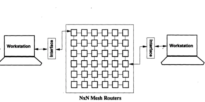
1.1 Interface Board Connecting Workstations to Routers...
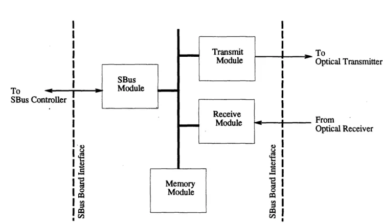
2.1 Block Diagram for the SBus Board Design ...
3.1 Transmit Module Signaling ... 3.2 Receive Module Signaling ... 3.3 SBus Module Signaling ... 3.4 CRC-12: Check Polynomial G(X) 3.5 CRC Logic Block ...
4.1 SRAM TDMA Cycles ...
4.2 Next FSM Signaling . .- ...
= X
12+ X
1 + X3 +X 2SBus Interface Signals Intermodular Signaling Next FSM ... SBus Module ... Transmit Module . . . Receive Module .... 3 5 9 10 11 13 13
+X+1
17 17 A.1 A.2 A.3 A.4 A.5 A.6 39 40 44 46 49 52...
...
...
...
Chapter 1
Introduction
As VLSI and packaging technology improve, the computing power delivered by a single processor has been increasing rapidly. The current generation of worksta-tions can deliver more power than mainframe computers a decade ago and in a more cost-effective manner. The productivity of these workstations could be increased even further by harnessing the aggregate power of multiple workstations connected in a network, thereby enabling researchers to develop new ways of using groups of these low cost and high performance workstations to deliver unprecedented comput-ing power. However, current network technologies cannot offer such options owcomput-ing to the following limitations:
1. Bandwidth. The most common local area network technology is implemented
by Ethernet. While Ethernet can deliver a maximum bandwidth of 10 Mbits/sec, the actual throughput is typically between 2 to 3 Mbits/sec [6]. Such a low bandwidth makes communication extremely expensive and seriously limits the capabilities of networked workstations.
2. Latency. Many interactive or real time applications require low latency. The high overhead of packet-switching protocols, such as the circuit set-up and tear-down time required by ATM, preclude their use in environments where commu-nication latency is critical.
3. Cost. There are numerous high speed network architectures being proposed
and ATM) have exceedingly high costs that prevent their widespread use in low budget situations.
This thesis provides a possible solution to the above stated problems by presenting the design of an interface board which connects a workstation to a router to form a low latency and high bandwidth network. The prototype board is a SPARC Bus (SBus) board connected to a SPARCStation. The use of SBus is motivated by the SBus' status as a popular industrial standard which provides low cost, compact form factor and high bandwidth transfer between the mother board and the card. The SBus system design also permits the use of a large installed base of SPARCStations at the AI Lab as a testbed.
To provide a clear picture of the functionality of the SBus board, let us consider the following scenario:
Suppose there is a network of SPARCStations as shown in Figure 1.1. Each of the SPARCStations is connected to an NxN mesh of routers through its own SBus board. If workstation A (host) wants to send a message to workstation B (destination) on the network, it writes to its SBus board which relays the message to the router via fiberoptic cable. The router delivers the message through the mesh network to the SBus board on B which then forwards the message to the kernel.
While the primary design objective of this thesis is to solve the above mentioned limitations of current network technologies, we also need to keep the following design issues in mind:
1. Transparency and Modularity. The board is intended to be an interface
connecting workstations to networks and it is important that this interface be well-defined and transparent (i.e. has a small number of handshake signals).
2. Small Form Factor. All the components must fit on a single-width SBus
expansion board (146.70mm x 83.82mm) given by the SBus specification. Thus, the parts count should be minimized to make the design more compact.
NxN Mesh Routers
Figure 1.1: Interface Board Connecting Workstations to Routers.
3. Ease of Implementation. Due to constraints of time and effort, ease of
implementation is clearly an important consideration. While we may choose to cut corners to increase the throughput or to lower the cost, it is important to ensure that the design remains robust. The design must effectively trade off constraints of speed, size, cost, ease of implementation and maintenance.
The thesis is organized into 7 chapters. Chapter 2 presents an overview of the SBus interface board and describes features of the system. Chapter 3 describes the various modules on the board while Chapter 4 turns to discuss the operation of the board and provides a detailed example of message flow. Chapter 5 describes the simulation used to verify the design. Chapter 6 presents the performance evaluation and the various design options of the work. Finally, Chapter 7 presents the conclusions.
Chapter 2
Design Overview
The SBus interface board is designed for a host-based system with a 32-bit I/O in-terface between the SBus system on a SPARCStation and a remote end connected to networks. A typical SBus system consists of three participants: an SBus master that initiates the transfer request, a slave that performs the operation and an SBus controller that oversees the whole SBus transaction. The SBus board in this thesis is implemented as an SBus slave that responds with an acknowledgment to Address Strobe and Slave Select asserted by the controller. However, the slave is not capa-ble of initiating an SBus transaction, except indirectly by generating an Interrupt Request. The words SBus interface board, SBus board and SBus slave will be used interchangeably in this thesis.
A detail specification of the SBus board is provided in Appendix A and the overall design is as follows:
* Clocking:
The SBus board operates at 25 MHz. This clock frequency provides a good balance between high performance and ease of system design and integration. It also satisfies the restriction imposed by the SBus clock which specifies the board to run between 16.67 MHz and 25 MHz. The FDDI ENcoder DECoder (ENDEC), due to its FDDI property however, performs at a frequency of 12.5 MHz. All of the modules on the SBus board are synchronized to the Nibble
I
To
Optical Transmitter
From
Optical Receiver
Figure 2.1: Block Diagram for the SBus Board Design.
* Logic Partitioning:
The SBus board consists of the following major logic blocks (refer to Figure 2.1):
1. Memory Module. The Memory module provides storage for messages de-livered among the SBus module, the Transmit module, and the Receive module.
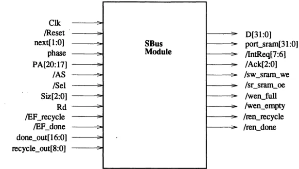
2. SBus Module. The SBus module serves as an interface between the SBus controller on the SPARCStation and the SBus board. It provides hand-shake signals to initiate transfer of data between the CPU master on the host machine and the SBus board.
3. Transmit Module. The Transmit module (Tx) is responsible for sending
messages and relinquishing buffers that have been transmitted. It also
To SBus Con I I I I I I : I :
generates a header word and a checksum for each message, and sends flow-control information to the Receive module at the remote end.
4. Receive Module. The Receive module (Rx) is the dual of the Transmit module. It is responsible for requesting buffers to handle incoming pack-ets, decoding the header packpack-ets, verifying the checksum, and relaying incoming flow-control signals from the remote end to the Transmit mod-ule.
* TDMA plan:
The SBus board is operated under the Time Division Multiplex Access (TDMA) plan. Under this protocol, access to the SRAM is time-multiplexed among the three logic blocks, namely.the SBus module, the Tx and the Rx.
The SRAM cycles are divided into the following cycles, during when a specific logic block has exclusive access to the SRAM
- Receive Cycle (Rx.cycle) - SBus Write Cycle (SWr.cycle) - Transmit Cycle (Tx-cycle) - SBus Read Cycle (SRdcycle)
The 12.5 MHz ENDEC constitutes a bottleneck of the system. Since 8 clock cycles are required to transmit and to receive a 32-bit word to and from the ENDEC, each logic block can only effectively access the SRAM once every 8 clock cycles. There are 4 SRAM cycles and thus, the optimal partitioning required for each SRAM cycle is 80 ns. The cycles on the board are orchestrated by three different Finite State Machines (FSMs), namely the Transmit FSM (Txfsm), the Receive FSM (Rxfsm) and the SBus FSM (SBusfsm). These three FSMs are coordinated by a Next FSM (Nxtfsm) which enforces the TDMA plan. The simplicity of the interfaces among the FSMs makes the SBus board easy to implement and debug.
Most of the FSM controls and interface logic are implemented in an Altera Erasable Programmable Logic Device (EPLD) for design customization and cost minimization.
While the design can be implemented using existing hardware components, such an approach will cause the board size to exceed the SBus form factor specification. Although one may resort to a double-sided card using surface mount technology, this would increase both the cost and the complexity of the design. Instead, we chose the Altera EPLD because it provides high-density logic integration, greater cost-effectiveness, shorter development cycles, a smaller board area requirement and better ease of modification.
Chapter 3
Board Modules
This chapter presents the details of the logic blocks described in the previous chapter. The functionalities of the Transmit module (Tx), the Receive module (Rx), the SBus module and the Memory module are discussed. Furthermore, the submodules inside each logic block are examined. The block diagrams and signal definitions of the modules are included in Appendix A.
3.1 Modules
The SBus interface board consists of the following four modules:
3.1.1 Memory Module
The SRAM memory is accessed by three logic blocks (SBus module, Tx and Rx) under the TDMA plan. It is a 4 megabit (128Kx32) memory cell and is divided into 512 1KByte buffers where each buffer can hold a maximum of 256 32-bit words. The 17-bit SRAM address is composed of a buffer pointer (9 bits) and an offset (8 bits) into the buffer.
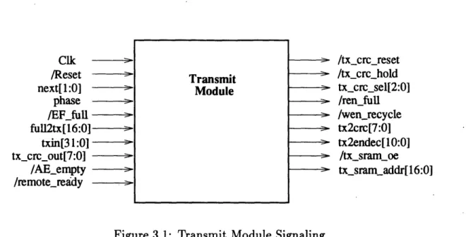
Clk /Reset next[ 1:0] phase /EFfull ful2tx[16:01 txin[31:0] tx_crc_out[7:0] /AEempty /remoteready /txcrc_reset /txcrc_hold tx_crcsel[2:0] /ren_full /wenjrecycle tx2crc[7:0] tx2endec[10:0] /txsram_oe tx_sramaddr[16:0]
Figure 3.1: Transmit Module Signaling
3.1.2
Transmit Module
The Tx is responsible for obtaining an address pointer to a full SRAM buffer and sending messages to the remote end. It reads a 32-bit word from the SRAM during the Tx-cycle, and transmits the word to the TxENDEC during the subsequent 8 clock cycles. Upon completing the transmission of the message, it puts the buffer pointer into a recycle FIFO and asserts an Interrupt signal to the SBus controller, which then returns the buffer pointer to the free-pointer queue in the kernel.
The Tx is composed of the followings:
* Multiplexor for selecting whether data, control bytes, or checksum is sent across the link.
* Parity generator for outputting the odd-parity bit to the TxENDEC. * Registers for synchronizing the inputs and outputs to and from the Tx. * TxENDEC for encoding 4B/5B code.
3.1.3
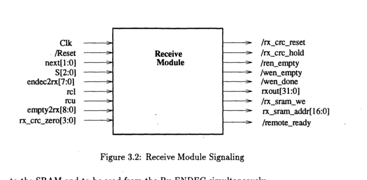
Receive Module
The Rx receives messages from the remote end and writes them to the SRAM during the Rx.cycle. It consists of a 2-deep 32-bit-wide FIFO which allows data to be written
Transmit Module i> 5-i-:.. M-i> _'V
i-Clk /Reset next[l :0] S[2:01 endec2rx[7:0] rcl rcu empty2rx[8:0] rx_crczero[3:0] /rxcrc_reset
/rxrc_hold
/renempty /wenempty /wen_done rxout[3 1:0] /rxsram_we rx_sramaddr[16:0] /remotereadyFigure 3.2: Receive Module Signaling to the SRAM and to be read from the RxENDEC simultaneously.
Upon completion of message reception, if there is no error in the received message, an Interrupt Request is generated to the SBus controller for transferring the message to the host machine. If an error is encountered during the receiving process, the Rx simply relinquishes the buffer by putting the buffer pointer back to an empty FIFO for later use.
The Rx is composed of the followings: * FIFO consisting of two registers:
- Register A for storing data from RxENDEC. - Register B for outputting data to SRAM.
* RxENDEC performing 4B/5B decoding of received data.
* RxEDS (ENDEC Data Separator) for recovering clock and data from the FDDI bit stream.
3.1.4 SBus Module
The SBus module consists of the SBusWrite submodule and the SBusRead submod-ule. The SBusWrite submodule is responsible for writing messages from the controller
Receive
Module
Clk /Reset next[ 1:0] phase PA[20:17] /AS /Sel Siz[2:0] Rd /EF_recycle /EF_done done_out[l16:0] recycleout[8:0] D[31:0] portsram[3 1:0] /IntReq[7:6] /Ack[2:0] /sw_sram_we /sr_sram_oe /wen_full /wen_empty /renrecycle /rendone
Figure 3.3: SBus Module Signaling
to the SRAM and the SBusRead submodule is responsible for reading messages from the SRAM to the controller. Since the traffic between the SBus controller and the slave SBus module is bidirectional, the datapath between the two employs tristate logic to avoid contention.
The SBus module is composed of the followings:
* sram2sbus tristate buffer for driving the SRAM data onto the SBus. * sram2sbus register for synchronizing the bus input from the SRAM. * sbus2sram tristate buffer for driving the SBus data to the SRAM. * sbus2sram register for synchronizing the bus input from the SBus.
3.2
Submodules
Within each module just described, there are submodules that complement the func-tions of the logic blocks.
SBus Module i- : i- :R-:O . ER-:O 3-
R-3.2.1
Bus Exchange Unit (Bux)
The Bus Exchange Unit is a multiple bus exchange device that time-multiplexes the SRAM datapath among the SBus module, the Tx and the Rx. The unit is organized as two I/O ports, one Input port and one Output port, where each port can be used as either a source or destination under independent control to implement a digital cross-point switch. This device facilitates the communication among the four ports: data can be routed from the SRAM to the Tx, from the Rx to the SRAM and between the SBus and the SRAM. Each port has a 16-bit databus. To form a 32-bit interface, two Buxes are cascaded together. This module is implemented in an Altera EPLD.
3.2.2 ENDEC
In both the Tx and the Rx, an ENDEC is used to perform 4B/5B encoding and decoding of data to and from the FDDI link. The TxENDEC enables line states to be forced onto the link for control purposes and the RxENDEC decodes line-state information from data that has been received from the fiberoptic link. The data frame is transmitted and is received in the form of 8-bit bytes accompanied by two control characters and one odd-parity bit. The ENDEC, which operates at 12.5 MHz, transmits or receives a byte of data every other clock, thus delivering a transfer rate of 100 Mbits/sec.
3.2.3 EDS
The ENDEC Data Separator recovers clock and data from an FDDI bit stream. It extracts the receive bit clock from the serial frames on the fiberoptic line. The EDS also provides timing information for the RxENDEC to perform 4B/5B decoding before sending data to the Rx.
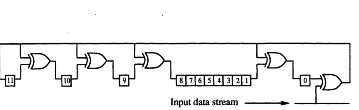
3.2.4
Cyclic Redundancy Checks (CRC)
The checksum mechanism is performed by 4 block check registers (BCRs) using the CRC-12 cyclic code [14]. The CRC-12 code provides error detection of all burst errors
Input data stream - I
Figure 3.4: CRC-12: Check Polynomial G(X) = X12 + X" + X3+ X2+ X + 1
Clk > /Reset > Crc_ln[7:0] / /Clear /Hold 8
.
>CrcOut[7:0]
4/ Zero[3:0] CrcSel[2:0]Figure 3.5: CRC Logic Block
of length 12 or less. The data length can be arbitrary. Thus, redundancy and coverage probability change with the data length.
Each BCR is implemented by a serial shift XOR circuit (Figure 3.4). Since a byte of data is transmitted every 2 clock cycles, 8 bits of data need to be serially shifted through the BCR circuit in 2 clocks. However, to avoid using a higher frequency clock, 4 BCR circuits are used in parallel, where each BCR circuit performs a checksum on 2 bits of data (as shown in Figure 3.5).
In operation, each TxBCR (Transmit BCR) is preloaded with an zero initial value. The data is simultaneously transmitted and fed to the input of the TxBCRs. Once the last data bit has been transmitted, the TxBCRs contain the check bits of the code word which are then transmitted following the data. Identical BCRs are used at the receiving end (also initialized with the same value as that used in the TxBCRs).
2 - 1 BCRO ZI
2~~~~~~~~1
BCR1 2 1 BCR2 BCR3 ll~~1The output of the RxENDEC is fed to the RxBCRs' (Receive BCRs') input. Similar to the TxBCRs, the received check bits are fed into the RxBCRs following the data bits. When there is no error in the message, the result in the receiver is zero.
Notice that checksum is performed only when data is transmitted from the SBus interface board to the remote end and when data is received from the remote end to the board. The link between the SBus controller and the SBus slave is assumed to be reliable and no checksum is performed.
This module is implemented in an Altera EPLD.
3.2.5
FIFOs
The memory is partitioned into 512 1KByte buffers. Upon initialization, half of the buffers are allocated for message transmission and half of the buffers are allocated for message reception.
The status of the buffers is monitored by both the kernel and the SBus slave. The SBus slave keeps track of the SRAM buffer status by means of the four FIFOs on board. Each buffer pointer can be in one of the following five states:
* Tx-Empty: ready to be written by kernel.
* Tx-Full: ready to be transmitted to the remote end.
* RxEmpty: ready to receive a message from the remote end. * Tx-Recycle: ready to be reclaimed by the kernel.
* RxDone: ready to be transmitted to the kernel. 1. Full FIFO
The Full FIFO contains the pointers and lengths of allocated SRAM buffers
whose contents are ready for transmission. The SBus controller writes the
buffer information into the FIFO after transferring data to the SRAM. The Tx then reads the pointers and transmits data to the remote end.
2. Empty FIFO
The Empty FIFO contains pointers to free buffers which are ready for reception of data from the remote end. When a message arrives, the Rx retrieves a free pointer from the Empty FIFO to store the message. The buffer pointer is returned to the Empty FIFO when:
(a) the SBus controller finishes reading the received message.
(b) the received message contains errors. (In this case, the incoming message is discarded.)
3. Done FIFO
The Done FIFO contains pointers to buffers which are ready to be transmitted from the SBus slave to the host machine. The Rx writes to the FIFO after receiving an error-free message. The FIFO is then read by the SBus controller to transfer data to the host machine.
4. Recycle FIFO
After the Tx finishes sending a message, it writes the transmitted buffer pointer to the Recycle FIFO. The Recycle FIFO is read by the SBus controller to reclaim the buffer for another data transmission.
Chapter 4
Board Operation
This chapter describes the operation of the logic blocks and details the means by which a message is sent to and received from the SBus interface board.
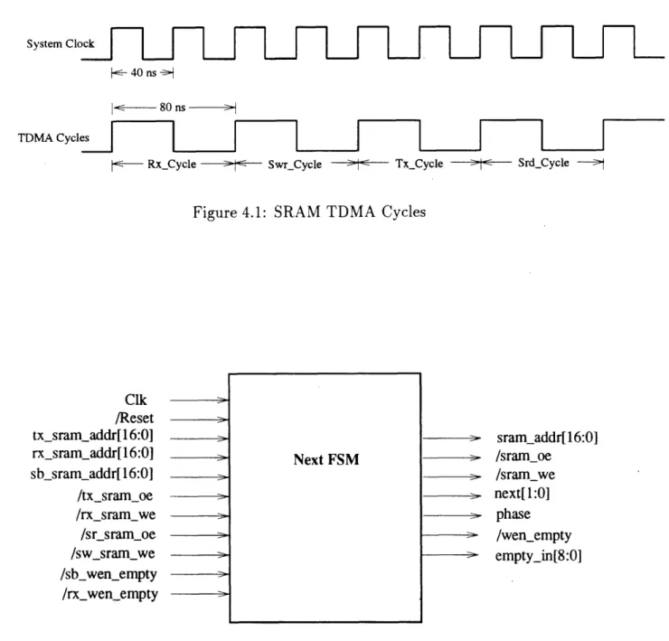
4.1 TDMA plan
Under the Time Division Multiplex Access (TDMA) plan, the SRAM is accessed by the Tx, the Rx and the SBus module during Tx-cycle, Rx-cycle, SRd-cycle and SWr.cycle (Figure 4.1). These four cycles are automated by a Next FSM performing
SRAM cycle partition and databus/addressbus arbitration. The Next FSM selects
which module drives the SRAM address and datapath, asserts (or deasserts) /WEand
/OE SRAM signals accordingly, and enables tristates and registers at the module
interface to guarantee that there is only one module driving the bus at any particular time (Figure 4.2).
4.2
The SBus Operation
The SBus slave in the design connects the host machine to the remote end. There are 8 handshake signals associated with data transfer between the SBus controller and the slave:
System Clock
-<- 40 ns
--jI - 80 ns -i
TDMA Cycles I I I
-: Rx_Cycle 3 Swr_Cycle ti TxCycle Tic SrdCycle
Figure 4.1: SRAM TDMA Cycles
Clk /Reset tx_sram_addr[ 16:0] rx_sram_addr[ 16:0] sb_sram_addr[ 16:0] /txsram_oe
/rxsramwe
/srsram_oe /swsram_we /sbwenempty /rxwen empty sram_addr[ 16:0] /sramnoe /sramwe next[ 1:0] phase /wenempty empty_in[8:0]Figure 4.2: Next FSM Signaling
Next FSM :O ii'- i-
3-· /AS (Address Strobe) : used by the SBus controller to initiate a slave cycle.
* /Sel (Slave Select): The SBus is a geographically-addressed bus. Each SBus
slave receives an unique unary encoded /Sel address signal. The assertion of
this signal indicates that the given slave is addressed.
* Rd (Read): signals whether the SBus controller will read data from the selected slave (Rd asserted) or write data to the slave (Rd unasserted).
* PA[27:0] (Physical Address): PA[16:0]is used to address the SRAM. PA[20:17] are used as flags to signal special conditions.
* Siz[2:0] (Size): used to indicate the number of bytes to be transferred to and from the SBus controller.
* D[31:O] (Data): transfer data and buffer pointers.
* /Ack[2:0] (Transfer Acknowledge): indicates the types of data that have been transferred (Data Ack), or that the current slave cycle should be terminated (Error Ack), or both.
* IntReq[7:1] (Interrupt Request): used by the SBus slave to request service
from the host machine.
4.2.1 The Slave Cycle
The slave cycle occurs when there is data transfer between the host machine and the slave. It ends only after the slave acknowledges the last word of data, or issues an Error Ack in response to a transfer size that it is unable to support. The slave cycle can be either one of the following two types:
1. SBusWrite Cycle
When writing data to a slave, the SBus controller drives the first datum onto the bus in the clock cycle when AS is asserted. At a later time (subject to timeout), the slave generates a Data Ack for one clock cycle.
2. SBusRead Cycle
When reading data from a slave, the slave can generate a Data Ack at any time (subject to timeout), beginning with the clock cycle following the assertion of /AS. The data corresponding to the acknowledgment is driven onto the databus for exactly one clock cycle during the clock cycle immediately following the Data
Ack.
4.2.2 Service for Interrupt Request
Interrupt Request (/IntReq[7: 1]) provides a mechanism for the SBus slave to interrupt the CPU. When the not-empty flag of the Done FIFO is asserted, the SBus slave asserts one of the Interrupt lines to asynchronously signal the CPU to read from the slave. After an Interrupt has been serviced, the SBus controller clears the asserted ,/IntReq line. The SBus slave, however, cannot deassert an Interrupt until polled by the controller. The SBus has a total of seven shared Interrupt lines which a slave can
assert at any time.
4.3 Message
Each message consists of a start delimiter, data, an end delimiter and a checksum codeword. The kernel is responsible for assembling the header information (such as destination and message length) into the data frame before handing the message to the SBus. The SBus board is responsible for providing a start delimiter and appending an end delimiter and a checksum at the end of each message frame. The message frame format is composed of the followings:
1. Idle bytes (16 or more bytes). 2. Start delimiter (4 control bytes). 3. Data (1 to 256 32-bits-word). 4. End delimiter (2 control bytes).
5. Checksum (6 bytes of CRC checksum)
4.3.1
Sending and Receiving a Message
The transmission of a message from a host begins with the assertion of Address Strobe (/AS) and Slave Select (/Selo) by the SBus controller. The buffer pointer to the SRAM is provided by the kernel of the host machine on the Physical Address (PA) lines. SBus starts writing the message to the SRAM. After the entire message is written, the buffer pointer and the message length are added to the Full FIFO. During the Tx-cycle, the Txfsm reads the pointer and message length from the Full FIFO and starts message transmission. Upon completion, the Txfsm writes the buffer pointer to the Recycle FIFO and asserts an Interrupt Request signal. When the SBus controller services the Interrupt Request, it returns the buffer pointer to the kernel for later use.
The reception of a message begins with the arrival of the start delimiter of a message frame. A free buffer pointer is retrieved from the Empty FIFO to store the received message. Upon receiving the end of a message, if there is no error in the message, the buffer pointer is written to the Done FIFO and an Interrupt Request is signaled. The SBus controller services the Interrupt by reading the received message from SRAM to host and freeing the buffer by returning it to the Empty FIFO.
We now turn to look at how a particular message flows among the different logic blocks on the SBus board.
1. Message Flow from the SBus Module to the Transmit Module
The Txfsm controls the message flow from the SBus module to the Tx. When the Tx has no message to send, the TxENDEC outputs idle bytes over the fiberoptic link to the remote end to indicate no valid data. At least 16 idle bytes are transmitted before any valid data is sent in order to synchronize the source TxENDEC and the destination RxENDEC. After completing the idle transmission, if the Full FIFO is not empty, the Txfsm sends a start delimiter followed by data and checksum. If the Full FIFO is empty, the Txfsm will return to the idle state and wait for the next message arrival.
2. Message Flow from the Receive Module to the SBus Module
The Rxfsm controls the message flow from the Rx to the SBus Module. The Rxfsm spins in the idle state until the start delimiter of a message is received. Data bytes are first put into Register A until a word is composed which will then be shifted into Register B. Register A is ready for receiving the next word and Register B is ready to be read by the SRAM. This process continues until the end of message is indicated. If there is no error in the message, the received buffer will be sent to the SBus module. If the received message contains an error, the buffer will be ignored and the buffer pointer will be reused for further message reception.
3. Message Flow between the SBus Module and the SBus Controller The SBusfsm controls the message flow from the SBus module to the SBus controller. The assertion of Address Strobe (/AS) and Slave Select (/Sel) by the controller indicates the beginning of a slave cycle when data is transferred between the SBus slave and the host machine. The physical address PA[27:0],
Rd, Siz[2:0] and D[31:0] (if performing a write) at this time are driven onto the bus. During an SBusWrite, a free buffer pointer is read from the kernel. Data is transferred from the controller to the slave and is written to the SRAM during SWR-cycle.
An SBusRead is performed in response to an Interrupt requested by the slave. Such Interrupts can serve for either reading data from the slave during the SRd-cycle or for returning transmitted buffer pointers back to the kernel. A Data Ack from the slave terminates the slave cycle.
4.4 Flow-Control
To prevent message overflow, a simple flow-control mechanism applies back pressure to the transmitting end when the receiving end is running out of buffers.
The Empty FIFO, which holds pointers to empty Rx buffers, asserts an almostLempty flag when the number of pointers in the FIFO is less then a predetermined number
(7, in our case). When the Tx detects the almosLempty flag, TxENDEC sends halt bytes in place of the normal control sequence.
At the remote end, when the Rx detects halt bytes in the incoming stream, it deasserts the remote-ready flag, causing the remote Tx to cease sending messages.
Eventually, when the SBus controller finishes reading the received messages from the SRAM, it returns the freed buffer pointers to the Empty FIFO, causing the almost-empty flag to be deasserted. When the Tx detects the deassertion of the almostLempty flag, it stops sending halt bytes and sends the normal byte sequence. When the remote Rx detects the normal control bytes in the message stream, it asserts remote-ready to enable the remote Tx to resume message transmission.
4.5 Interface to the SunOS
The software in the SPARCStation kernel is responsible for the followings:
* Assembling any header information (such as destination and message length) required by the routers in data frames.
* Keeping a list of free-buffer pointers. When there is a message to send, it obtains a free buffer pointer and generates the corresponding SRAM address on the address lines (PA[16:0]).
* Asserting PA[17] to indicate End Of Write after a message is sent to the slave. * Asserting PA[18] to indicate End of Read after a message sent from the slave is read. The freed buffer pointer is returned to the Empty FIFO for later use. * Asserting PA[19] when servicing Interrupt Request[7] (/IntReq[7]), the request
for message transfer from the Rx to the SBus controller.
* Asserting PA[20] when servicing Interrupt Request[6] (/IrtReq[6), the request for reclaiming a freed buffer pointer from the Recycle FIFO.
Chapter 5
Simulation
5.1 Generation of Simulation Results
To verify the correctness of the SBus interface board and to obtain timing information, modules were written in Verilog and Altera Hardware Description Language (AHDL) to model the components' behavior on the board.
The models of the SBus controller, the SRAM, the FIFOs and the ENDEC were written in Verilog. To reflect the real behavior of each component, timing constraints (such as signal hold-time and clock-to-data-valid latency) as specified in the data sheet were modeled as closely as possible in each of these modules.
The Txfsm, the Rxfsm, the SBusfsm, the Nxtfsm and the CRC submodule were written in AHDL and compiled into Edif files using the Altera MaxplusII software. The Edif files were converted to Verilog for simulation.
Each of the above modules was simulated, debugged and modified with separate drivers and test vectors in isolation before all modules were integrated for the final simulation.
5.2 Simulation Results
A loopback simulation was used to validate the operation of the SBus interface board. The operation of sending and receiving a message, as described in the previous
chap-ters, was verified in the following loop:
1. SBus Controller to SRAM: Messages are generated by the SBus controller connected to the SBusfsm. The SBusfsm writes the data from the controller into a SRAM buffer specified by the controller. When the End of Write (EOW)
is detected, the buffer pointer and length are written to the Full FIFO.
2. SRAM to Tx: The Tx constantly monitors the Full FIFO for message arrival. When the Full FIFO is not empty, the Tx fetches the first buffer pointer in the queue and transmits the message to the TxENDEC.
3. Rx to SRAM: To form a loop, the TxENDEC is looped back to the RxENDEC. When the Rx detects the start delimiter of a message, it retrieves a buffer pointer from the Empty FIFO for the incoming message. When an error-free message is received, the Rx writes the pointer to the Done FIFO.
4. SRAM to SBus Controller: The SBusfsm monitors the Done FIFO for
message arrival. When the Done FIFO is not empty, the SBusfsm asserts an Interrupt Request to the SBus controller. The SBus controller then reads the message from the SRAM and verifies the correctness of the message.
To avoid any a priori assumptions, the message lengths, contents and arrival times are generated by random number generators provided in Verilog, allowing the message arrival at the SBus controller to be at a random time, of random length and with random content.
5.2.1 Verification of TDMA Plan
Since each module of the SBus board operates concurrently, the SBus controller can be writing a message to the memory module while the Tx is transmitting a second message and the Rx is receiving a third message. The proper functioning of the TDMA was verified by examining the multiplexed signals which drive the memory module and the interleaving reads and writes initiated by the various modules.
5.2.2 Verification of Flow-Control
In order to verify the flow-control mechanism, the size of the Empty FIFO was ad-justed to simulate a low-memory condition. The Empty FIFO was initialized to contain 8 buffer pointers.
The flow-control mechanism was tested as follows: 1. SBus controller writes a message to SRAM.
2. Tx transmits the message to Rx (due to the looping of messages in simulation). 3. Rx detects the message and retrieves a buffer pointer from Empty FIFO, causing
the almost-empty flag to be asserted.
4. Tx detects the almost-empty flag and sends halt bytes in place of idle bytes (if in the idle state), or in place of the start control bytes (if transmitting the start delimiter) or in place of the CRC control bytes (if transmitting the CRC sequence).
5. Rx detects halt bytes in the incoming bit stream and deasserts remote-ready. 6. Tx (after sending its current message) detects the deassertion of remote-ready
and sends halt bytes, even if there are pending messages in the Full FIFO. 7. After reading the message from SRAM, the SBus controller frees the buffer by
returning its pointer to Empty FIFO.
8. Empty FIFO deasserts the almost-empty flag (because there are now more than 7 buffer pointers in the FIFO).
9. Tx detects the deassertion of almost-empty and sends the normal control bytes, instead of the halt bytes.
10. Rx detects the normal control bytes in the incoming bit stream and asserts
remote-ready.
11. Tx detects the assertion of remote-ready and resumes message transmission if there is any pending message in the Full FIFO.
Thus far, no mention has been made of the simulation of the SBus interface board under different network traffic conditions. The network traffic can be modeled in Verilog simulation. This can be accomplished by using queueing models which use predicted job creation and processing rates to simulate the operation of the system under varying loads. The jobs' arrival rates and processing times can be represented by random functions which approximate the real world. Meanwhile, dynamic infor-mation concerning the current and maximum queue length, mean inter-arrival time and average waiting time can be gathered. Verilog provides random number gen-erators which return integer values distributed according to standard probabilistic functions, such as Exponential, Poisson, and Erlang functions. Although the analysis remains to be done, this kind of stochastic network traffic analysis offers the potential for insights into the performance ramifications of the board design.
Chapter 6
Performance Evaluation and
Design Options
Previous chapters explained the details of the physical components and operation of the SBus interface board. This chapter presents a performance evaluation of the board.
6.1 Performance Evaluation
6.1.1
Throughput
The SBus board adopts a host-based design supporting only single word transfer (i.e. non-burst mode). Operating at 25 MHz, the peak transfer rate of the SBus controller
is 100 MBytes/s. With single word transfer mode between the SBus controller and the board, the effective I/O bandwidth is approximately 33 MBytes/s, since each SBus transaction requires three cycles: address strobe, data transfer and acknowledgment. lTo evaluate the performance of the Tx and the Rx, we define the protocol efficiency,
, as follows:
length of data
For data length and protocol overhead r, the efficiency r is given by the following equation:
1
= r +l
The overhead, , included in every message is fixed at 7 words (4 words of control bytes, 1 word of start delimiter and 2 words of end delimiter and checksum).
Due to the lack of real application statistics concerning message data lengths, the ef-ficiency is computed under several assumptions regarding the probability distribution of data lengths (in words), Pr(l):
1. Pr(l) is uniform or Gaussian with the expected data length, E[l], equals 128.
The efficiency 128 i about 95%.
2. Pr(l) is a shifted Gaussian with the expected data length, E[l], equals 64. The
efficiency 764 is about 90%.
3. Pr(l) is a shifted Gaussian with the expected data length, E[l], equals 32. The
efficiency 7732 is about 80%.
Thus, after excluding the protocol overhead, the Tx and the Rx are capable of trans-rnitting and receiving at an average rate of 80-95 Mbits/s, when data lengths are longer than 32 words. The bandwidth is significantly better than those of the exist-ing LAN architectures. For example, the peak transfer rate of Ethernet is 10 Mbits/s
[6], while the peak transfer rate of Token Ring is either 4 or 16 Mbits/s [7]. The transfer rate of the SBus board interface is comparable to that of FDDI, since both of them operate in the range of 80-95 Mbits/s [16]. However, FDDI and our intended network design use different network topologies and exhibit different scaling proper-ties. The FDDI network is a ring network. The addition of workstations will degrade the performance of the ring and will eventually saturate the network. On the other hand, the SBus board is intended to be used in a network with a fast centralized switching hub whose performance will be less sensitive to an increase in network size.
The ATM packet-switching architecture is composed of 53-byte cells where each cell consists of 5 control bytes. Hence the efficiency of ATM network is approximately
90%, which is comparable to 7764 calculated above. ATM is a scalable architecture
permitting Gbits/s data transfer. The most common rate that is being used currently
is OC-3 (155.52 Mbits/s) which delivers a throughput of 140 Mbits/s. One can
see that the ATM offers a better performance when compared to the SBus board. However, the higher throughput is achieved at a higher cost, since the ATM chip sets are fairly expensive.
6.1.2
Latency
Another performance metric by which the SBus board can be judged is message latency, which we define as the time elapsed between the first word written to the SBus board by the sender and the last word read from the destination SBus board by the receiver.
As described in Chapter 4, a message transfer from host A to host B (each equipped with an SBus board) requires the following steps:
* Step 1: Host A to Memory on SBus board A. The message is written from host A to its SBus board memory.
* Step 2: Memory to Tx. The message is retrieved by the Tx and sent to the router.
* Step 3: Routing. The router delivers the message to the SBus board at host B. * Step 4: Rx to Memory. The message is written to the SBus board memory by
the Rx at host B.
* Step 5: Memory on SBus board B to host B. The message is read by host B from the SBus board.
To derive the latency due to the SBus board in the process above, the routing time is ignored since it is independent of our board design. We define board latency, T, as
the amount of time that data resides on the SBus board, i.e. message latency minus routing time. Assuming that the length of a data frame is words long, the steps in
a message transfer involving the SBus board require the following numbers of clock
cycles:
* Step 1: 8 x 1. A word is written from host A to the SBus board A once every 8 clock cycles (during SWR-cycle).
* Step 2: 8 x ( + r), where r is the protocol overhead (section 6.1.1). The
TxENDEC transmits one word every 8 clock cycles.
* Step 4: 8 x ( + r). The RxENDEC receives one word every 8 clock cycles.
* Step 5: 8 x 1. A word is read from the SBus board B by host B once every 8 clock cycles (during SRdcycle).
The protocol overhead r was calculated to be 7 words in section 6.1.1. For the purpose of latency calculation, step 4 can be considered as overlapping in time with step 2 (which can be seen if the routing time is assumed to be 0 for example), the board latency of message length 1, T, is given by the following equation:
T = 81+8(l+7)+8+81
=
241+64
In order to see the order of magnitude of the board latency, T is computed for three different values of l:
* l = 32: T equals 832 cycles or 33 psec. The shortest possible time required by
a 32-word transfer over a fiberoptic link is approximately 10 usec.
* I = 64: T equals 1600 cycles or 64 sec. The shortest possible time required by
a 64-word transfer over a fiberoptic link is approximately 21 /ILsec.
* I = 128: T equals 3136 cycles or 125 sec. The shortest possible time required
The latency figures above underscore the fact that the board latency is largely due to the buffering of messages between the host machine (or more precisely the SBus controller) and the board. The buffering is necessary due to the following two con-siderations:
1. The host machine may compose several messages simultaneously.
In deriving the board latency, it is assumed that the host writes the data words of a message consecutively. However, the host machine may in fact compose several messages at the same time. For example, the board memory may be directly mapped into the host machine's address space (to avoid copying) and several applications may simultaneously use the mapped memory to compose their messages. The supp6rt of such a technique of message creation requires buffering.
2. The SBus controller may take an arbitrary amount of time to service a request asserted by the SBus board.
Because the SBus is generally shared by multiple SBus devices, buffering of messages is essential. The SBus controller may need to service other SBus devices on the bus, and therefore may take an arbitrary amount of time to service requests asserted by the SBus board.
6.2 Design Options
The SBus system described in this thesis can be improved in several ways. Some of the more important of these possibilities are described below:
1. Higher Throughput
As the memory module can deliver 100 MBytes/s I/O bandwidth and greatly exceeds the current requirement of the SBus module, the Tx and the Rx, the bandwidth of the board can be easily increased by two-fold.
With the TDMA plan, one-fourth of the SRAM bandwidth is available to the Tx, another one-fourth to the Rx, and the remaining to the SBus module. The
Tx and the Rx can double their throughputs and fully utilize their SRAM band-width by each making use of a pair of ENDECs. To complement this change, the SBus module can also increase its throughput to 50 MBytes/s by using dou-ble word burst mode transfer. Assuming that the number of messages sent from the board roughly equals the number of messages received, the throughputs of the SBus controller, the Tx and the Rx will be balanced in this case (in the sense that none of the subsystems presents a bottleneck for others).
While the throughput can be easily improved by a factor of two, the options for attaining a yet higher performance are not as straight-forward. Such a goal would require significant redesign to improve the bandwidth of all parts of the board. One way to achieve the goal is to separate the Tx from the Rx by requiring each block to have its own SRAM and FSM logic. While increasing the transfer rate, such a technique may require two SBus expansion slots instead of one. This option limits the flexibility of the SBus expansion system and may not be a practical solution.
Notice that the peak data rate of an SBus system is 100 MBytes/s. A host-based SBus provides burst transfers of up to 16 words with two clock cycles of overhead, yielding a burst transfer rate of 88 MBytes/s. If this throughput of the SBus system is judged to be inadequate, a different computer architecture could be exploited for higher data bandwidth. For instance, the Alpha architecture delivers better performance and higher throughput than a SPARCStation and an increasing number of system developers are adopting the Alpha architecture. Unfortunately, the design of a high bandwidth Alpha interface would require very careful engineering.
2. Error Detection and Frame Resend
In the present system, when the Rx detects an error in a received frame, the message is immediately dropped. Therefore, the responsibility of retransmission is delegated to the application software and no resend mechanism is provided. The performance of the interface can be improved by having a link-level retry if an error frame is received. However, since fiberoptic cables, which have very low error rate (approximately 10-12), are used as the transmission media, the
Chapter 7
Conclusion
This thesis presented the design of a SPARC Bus interface board. The board is intended as an expansion board in any SBus system. It requires a minimal number of handshaking signals and features a very simple flow-control protocol. The modular design allows the system to be treated as a black box which is capable of connecting any SBus system into a network of arbitrary size.
The current design effectively trades off constraints in speed, size, cost and ease of implementation. As mentioned in Chapter 6, it is possible to adopt a system with higher performance in terms of speed and bandwidth, but only at the cost of dealing with a more complex and expensive design.
In summary, the design objectives stated in the Introduction were fulfilled in the following ways:
* High Bandwidth: The peak transfer bandwidth that the SBus board supports
is 100 Mbits/s. This is permitted by the use of the FDDI protocol and a
fiberoptic link.
* Compact Form Factor: Most of the logic on the board is implemented in an Altera EPLD, permitting a densely integrated system. In addition to the EPLD, only a handful of devices are required on the board: memory devices,
FDDI Encoder/Decoders and optical transmitter/receiver. The components
* Ease of Implementation and Maintenance: The board provides trans-parency among modules and facilitates modification and debugging. It is de-signed in a modular fashion (SBus module, Tx and Rx), and each module needs only to know the interface signals (rather than the internal operation) of other modules. This gives the designer the flexibility to modify and debug each sub-system independently, as was done during the simulation and verification phase of the board.
* Low Protocol Overhead: We have adopted a simple protocol which incurs little overhead in transferring messages. For the average message lengths be-tween 32 to 128 bytes, the overhead is 5% to 20%. As described in Chapter 4, flow-control handshaking information is piggybacked onto the control bytes in the message stream, thereby incurring no extra overhead.
Several lessons were learned from this project. First, one should start with a simple design and improve upon it. The original design objectives were ambitious in terms of transfer rate, flow-control and link-level error recovery mechanisms, which made the project difficult to implement. While the revised objectives for the project were more humble, they allow us to come up with a design which can be improved upon readily (as mentioned in the previous chapter).
The second major lesson learned was to expect bugs in software. The Altera Max-plusII compiler has numerous problems in compiling big modular designs (for instance, Txfsm) and some of them were very hard to detect. (For example, the compiler could
not compile correctly when the module had a certain number of states.)
In conclusion, this thesis presented the design of a prototype interface board which represents a stepping stone towards the goal of developing local area supercomputing. It serves as an indicator that the goal of having powerful and tightly-coupled networks can be realized in the future.
Bibliography
[1] Advanced Micro Devices. The SUPERNET Family for FDDI. 1991/1992 World Network Data Book.
[2] Advanced Micro Devices. Ethernet/IEEE 802.3 Family 1992 World Network
Data Book.
[3] Altera. Application Handbook, 1992. [4] Altera. Data Book, 1993.
[5] Altera. MAX+PLUS II Text Editor & AHDL, 1991.
[6] Computer Design, High-performance networks challenge Ethernet. July 1992, P77-92.
[7] Dimitri Bertsekas and Robert Gallager. Data Networks. Second Edition, Pren-tice Hall, 1992.
[8] Robert H. Halstead, Jr. 6.033 Notes on Networking and Communication, 1987. [9] Integrated Device Technology, Inc. Specialized Memories and Modules. 1992
Data Book.
[10] James D. Lyle. SBus, Information, Applications, and Experience. Springer-Verlag New York, Inc., 1992.
[11] Robert M. Metcalfe and David R. Boggs. Ethernet: Distributed Packet Switch-ing for Local Computer Networks. Communications of the ACM, C-19(7); 395-404, July 1976
[12] Craig Partridge. Gigabit Networking. Addison-Wesley, 1994.
[13] Michael D. Schroeder et al. Autonet: A High-Speed, Self-Configuring Local Area Network Using Point-to-Point Links. IEEE Journal on Selected Area sin
Communications. Vol.9, No.8; 1318-1335, October 1991.
[14] Daniel P. Siewiorek and Robert S. Swarz. Reliable Computer Systems, Design and Evaluation. Second Edition, Digital Press, 1992.
[15] Sun Microsystems. SBus Specification B.0, 1990.
[16] Andrew S. Tanenbaum. Computer Networks. Second Edition, Prentice Hall, 1989.
Appendix A
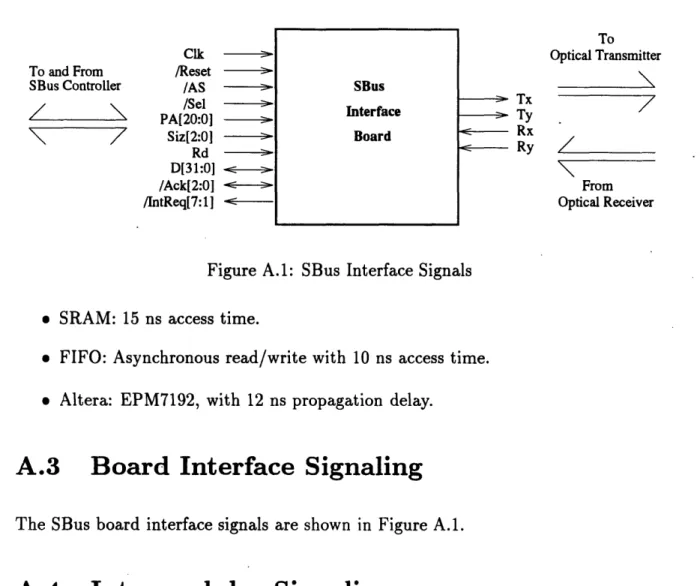
SBus Interface Board Specification
A.1
Device Components
* FDDI ENDEC: Part Number AM7984A (Advanced Micro Device). * FDDI EDS: Part Number AM7985A (Advanced Micro Device).
* SRAM: 4 megabit memory cell (128K x 32). Part Number IDT7M4013 (Inte-grated Device Technology).
* FIFO: 256 x 9-bit parallel SyncFIFO with clocked read and write controls. Part number IDT72201 (Integrated Device Technology).
* Altera EPLD: MAX 7000 Programmable Logic. Part Number EPM7192 (A1-tera).
A.2
Device Timing
The timing specification of each component is as follows:
* System Clock: 25 MHz, aligned to the Nibble Clock of the ENDEC. * ENDEC Clock: 12.5 MHz.
To and From SBus Controller Clk /Reset /AS /Sel PA[20:0] Siz[2:0] Rd D[31:0] /Ack[2:0] /IntReq[7: 11 Tx Ty c< Rx Ry To Optical Transmitter
\
/ From Optical ReceiverFigure A.1: SBus Interface Signals * SRAM: 15 ns access time.
* FIFO: Asynchronous read/write with 10 ns access time. * Altera: EPM7192, with 12 ns propagation delay.
A.3 Board Interface Signaling
The SBus board interface signals are shown in Figure A.1.
A.4
Intermodular Signaling
The top level module interconnection among SRAM, Tx, Rx, and SBus module is shown in Figure A.2.
A.5
Format of Message Frame
The format of a message frame is closely related to that of the FDDI Encoding Table [1]. During normal operation when there is no back pressure applied to the Tx, the message frame format is as follows:
SBus Interface
1. Idle bytes (16 or more IDLE-bytes).
2. Start delimiter (a JK-byte followed by 3 ZERO.bytes). 3. Data (1 to 256 32-bits word).
4. End delimiter (2 JK.bytes).
5. Checksum (6 bytes of CRC checksum).
When the flow-control mechanism applies back pressure to the Tx, the message frame format becomes the followings:
1. Halt bytes (16 or more HALT-bytes).
2. Start delimiter (a JK.byte followed by two ZERO-bytes and a HALT-byte). 3. Data (1 to 256 32-bits words).
4. End delimiter (a JK.byte followed by a HALT-byte). 5. Checksum (6 bytes of CRC checksum).
A.6
Memory Module
Name
11
/0 Descriptionaddr[16:0] I Address lines.
io[31:0] I/O Data lines for SRAM content.
/we I Write enable.
/oe I Output enable.
The SRAM module (implemented in Verilog) has 128K x 32-bit memory cells. The addr[16:0] addresses a particular cell whose content is output when oe is asserted, or the cell is written with data on io[31:0] when /we is asserted.
A.7
FIFO
There are 4 FIFOs on the SBus board, namely: 1. Empty FIFO (256 x 9-bit)
2. Recycle FIFO (256 x 9-bit) 3. Full FIFO (256 x 17-bit) 4. Done FIFO (256 x 17-bit)
Empty FIFO and Recycle FIFO are used to keep track of buffer pointers, so a 9-bit port is sufficient. Full FIFO and Done FIFO are used to record both the buffer pointers and length of messages, hence a 17-bit port is required.
Each FIFO FIFO):
has the following I/O signals (where W is the respective width of each
Name ] I/O Description
Wclk I Write Clock.
Rclk I Read Clock.
/reset I System reset.
in[W:O] I FIFO input.
out[W:O] 0 FIFO output.
/ren I Read enable.
/wen I Write enable.
/ef 0 Empty flag.
/ff 0 Full flag.
/ae 0 Almost-empty flag.
/af 0 Almost-full flag.
The FIFOs are capable of asynchronous Read/Write, i.e. it can service both Read and Write simultaneously.
The empty flag (/eJ) and the full flag (/ff) are asserted when the FIFO is empty and
full respectively. The programmable flags almost-empty (/ae) and almost-full (/af) are asserted when the FIFO contains (7) or (Full - 7) items respectively.
A.8 Next FSM
Name I/O Description
sysclk I System clock.
/reset I System reset.
tx sramaddr[16..0] I SRAM address driven by Tx.
rx-sramaddr[16..0] I SRAM address driven by Rx.
sbsramaddr[16..0] I SRAM address driven by SBus module.
/rxsramwe I SRAM write enable driven by Rx.
/swsramwe I SRAM write enable driven during a SBusWrite.
/txsramoe I SRAM output enable driven by Tx.
/srsramoe I SRAM output enable driven during a SBusRead.
sramaddr[16..0] O SRAM address.
/sramoe O SRAM output enable.
/sramwe O SRAM write enable.
/sbwenempty I Empty FIFO write enable driven by SBus module.
/rxwen _empty I Empty FIFO write enable driven by Rx.
/wenempty O Empty FIFO write enable.
emptyin[8..0] O Empty FIFO input.
next[1..0] O Current TDMA cycle.
phase O Phase (0 or 1). of the current TDMA cycle.
The Nxtfsm is the coordinator for the SBusfsm, the Txfsm and the Rxfsm. It gen-erates next[l:0] and phase signals to indicate the current TDMA cycle. During a particular TDMA cycle, inputs from the specified FSM are driven onto sramaddr, /sramoe and /sram-we. The Next FSM also coordinates the Writes from both the
Clk /reset Tx_sram_addr[ 16:0] Rx_sram_addr[ 16:0] Sw_sram_addr[16:0] Sr_sram_addr[16:0] /rxsram_we /swsram_we /txsram_oe /srsram_oe /sbwenempty /rxwenemtpy I__ *next *next *next *next
*next signal is generated internally in Next FSM > sram_addr[16:0] - next[l:0] - phase /sramoe - 0a1i41iwr empty_in[8:0] /wenemtpy
Figure A.3: Next FSM
--
---, "'