HAL Id: hal-01933414
https://hal.archives-ouvertes.fr/hal-01933414
Submitted on 23 Nov 2018
HAL is a multi-disciplinary open access
archive for the deposit and dissemination of
sci-entific research documents, whether they are
pub-lished or not. The documents may come from
teaching and research institutions in France or
abroad, or from public or private research centers.
L’archive ouverte pluridisciplinaire HAL, est
destinée au dépôt et à la diffusion de documents
scientifiques de niveau recherche, publiés ou non,
émanant des établissements d’enseignement et de
recherche français ou étrangers, des laboratoires
publics ou privés.
Advanced analysis of transient overvoltage in
electromechanical chain fed by SiC inverter
Bouazza Taghia, Bernardo Cougo, Hubert Piquet, David Malec, Antoine
Belinger, Jean-Pierre Carayon
To cite this version:
Bouazza Taghia, Bernardo Cougo, Hubert Piquet, David Malec, Antoine Belinger, et al.. Advanced
analysis of transient overvoltage in electromechanical chain fed by SiC inverter. Electrimacs 2017, Jul
2017, Toulouse, France. pp.0. �hal-01933414�
OATAO is an open access repository that collects the work of Toulouse
researchers and makes it freely available over the web where possible
Any correspondence concerning this service should be sent
to the repository administrator:
tech-oatao@listes-diff.inp-toulouse.fr
This is a
paper
published in:
http://oatao.univ-toulouse.fr/20808
To cite this version:
Taghia, Bouazza and Cougo, Bernardo and Piquet, Hubert
and Malec, David and Belinger, Antoine and Carayon,
Jean-Pierre Advanced analysis of transient overvoltage in
electromechanical chain fed by SiC inverter. (2018) In:
Electrimacs 2017, 4-6 July 2017 (Toulouse, France)
ELECTRIMACS 2017, 4th -6th July 2017, Toulouse, France
A
DVANCED
A
NALYSIS OF
T
RANSIENT
O
VERVOLTAGE IN
E
LECTROMECHANICAL
C
HAIN
F
ED BY
S
I
C
I
NVERTER
B.TAGHIA
1, 2, B.COUGO
1, H.PIQUET
2, D. MALEC
2, A.BELINGER
2, J.P.CARAYON
11. IRT Saint-Exupéry, 118, route de Narbonne - CS 44248, 31432 Toulouse cedex 4, France 2. LAPLACE, Université de Toulouse, CNRS, INPT, UPS, 2 rue Charles Camichel, 31071 Toulouse, France
E-mail: bouazza.taghia@irt-saintexupery.com
Abstract - Key areas in the development of More Electrical Aircraft (MEA) are, currently, DC power distribution in higher voltage levels and the use of disruptive technology such as Wide BandGap (WBG) semiconductor. Using WBG components (SiC and GaN) increases the power converter mass density. However, fast switching of WBG components (tens of kV/µ s) induces voltage transient overshoots due to parasitic coupling within the inverter. In addition, propagation and reflection phenomena along the harness, even for small lengths, cause voltage overshoots across the loads. Such overvoltage in an electromechanical chain (association of inverter, harness and motor) supplied by the new HVDC 540V aeronautical network could be fatal for the Electrical Insulation System (EIS). This paper proposes an accurate and fast model to predict overvoltage along a harness; it allows to analyze the impact of SiC inverter output voltage waveforms.
Keywords – Overvoltage, SiC inverter, Frequency modeling, More Electrical Aircraft (MEA).
1. I
NTRODUCTIONBackground:
The progressive replacement of hydraulic and pneumatic circuits by electrical systems [1], together with the rationalization of electrical energy result in a considerable gain of mass in modern aircrafts. In order to effectively respond to the growing need in electrical energy, the voltage level aboard new aircraft generations has grown from 115VAC to 230VAC. This has given rise to a new HVDC +/- 270V instead of +270VDC.
However, this new voltage level, combined with transient overvoltage along the harness (from the output of the inverter to the supplied load) and with aeronautical constraints, such as low pressure and high temperature, can be fatal for the Electrical Insulation System (EIS), which lifetime can be reduced by partial discharges and breakdown. Wide Bandgap (WBG) semiconductor technologies (Silicon Carbide – SiC, and Gallium Nitride – GaN) are currently under evaluation to be used in converters for motor drives in MEA. These inverters can be localized close to the motors, or deported (usually in pressurized area). In the second case, the connection between the inverters and the motor is ensured by a power cable called “harness”. In such electromechanical chain, high transient overvoltage at the motor terminals can appear; the latter are even increased by the use of fast WBG semiconductors, such as SiC MOSFETs. This paper presents a study
aiming to predict overvoltage at any point of the electromechanical chain right from the design phase. Scope and outline of the work:
Since the beginning of the 20th century, the problem of transient overvoltage has been particularly addressed in the field of electric power transport. They are caused in particular by the switching of the semiconductors and by the lightning aggression. Since the emergence of IGBTs in the late 1980s, this problem has started to be addressed in relation to an electromechanical chain [2, 3].
In this paper, we focus on the overvoltage caused by the harness. We have developed a distributed parameter model of harness. It is accurate, nonlinear with respect to frequency, very fast and can also be easily coupled with a model of the inverter and that of the motor.
2. T
RANSIENT OVERVOLTAGE MODELINGAlmost all the works dealing with overvoltage in the literature simplifies the electromechanical chain (generally a three-phase system) to an equivalent two-phase system. It is assumed that the inverter modulator only switches one leg inverter at a time. Then, for the case of three-phase inverter with three legs, there are always two parallel legs of inverter in steady state with a return third leg that is switched. According to [3, 4], , using this hypothesis, the modeling by an equivalent two-phase line gives satisfactory results. Thus, since the objective in this paper is not to study the effects of multi-conductor
electromagnetic cross-talk phenomenon on overvoltage, we will adopt the two-phase system modeling.
2.1.TRANSMISSION LINE HARNESS MODEL
The basic cable model used to analyze overvoltage is based on a temporal lossless two-conductor transmission line model, characterized by a propagation delay and a characteristic impedance . This approach is derived from the domain of telecommunications [5], and the waves theory. In this approach, the inverter is considered as a voltage source with a series impedance (almost always neglected); the cable is terminated by a load impedance which represents the motor (it is often assumed to be higher than 1kΩ).
The difference between the line characteristic impedance and its two termination impedances (called an “impedance mismatch”) causes the phenomena of wave reflections.
The overvoltage is thus the result of summing incident inverter voltage waves and reflected waves traveling between the inverter and the motor. The lossless transmission line assumption is often adopted, and and parameters are generally assumed to be independent of the frequency (non-dispersive line), which leads to inaccuracies. Moreover, the iterative nature of a time-based resolution can generate cumbersome computation time. For that reason we select a frequency domain simulation approach.
2.2.FREQUENCY MODELLING OF THE HARNESS
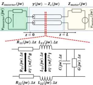
The harness is described by a two-conductor frequency model (Fig. 1), characterized by its primary parameters: ( ) and by its secondary parameters: propagation function ( ) and the characteristic impedance ( ). is the complex operator ( = −1) and is the angular frequency.
Fig. 1. Proposed equivalent two-phase model of electromechanical chain.
The harness (Fig. 1) chain-parameter matrix ( , = ) is obtained from an exact mathematical solution of the two-conductor propagation equations [6]. It can be written as follows, being the position:
( , ) ( , ) = ( , ) ( , 0)( , 0) = ( , )( , ) ( , )( , ) ( , 0)( , 0) Equation 1 where: ( , ) = !"ℎ( ( ). ) ( , ) = − " %ℎ( ( ). ) ( , ) = − " %ℎ( ( ). ) / ( , ) = !"ℎ( ( ). ) '' '' ( ) = () ( ) + ( )+( ( ) + ( )) ( ) = ,) ( ) +( ) + ( )+( ) ( ) = --( ) + ( ) − - ( ) − - ( ) ( ) = --( ) + ( ) − - ( ) − -( ) Equation 2
The parameters introduced in Equation 2 are represented on the electrical circuit of Fig. 1. Based on the superposition theorem, the only drawback of this model lies in the difficulty of taking into account the non-linearity effects with respect to the current and/or voltage (saturated inductance, diode...)[6]. This will not be considered in this work. Note that, this approach allows to easily take into account frequency effects (skin and proximity effects) on the harness parameters.
The inverter is modeled as a voltage source with series impedance and the motor as a back electromotive force ./0/1(23) with series impedance. The inverter, the harness and the motor models are concatenated by simply multiplying their chain parameter matrix. The voltage ( ( , )) and the current (( , )) quantities at position are computed from their values at the input of the cable (at = 0).
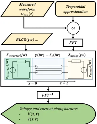
Fig. 4 summarizes the frequency resolution algorithm adopted in this work. It calculates the steady-state voltages and currents at any point of the harness in an extremely fast way (few seconds). The inverter voltage can be either derived from measurement or a priori defined waveform approximation (usually trapezoidal) (Fig. 4).
ELECTRIMACS 2017, 4th -6th July 2017, Toulouse, France
Test bench and characterization method used for measurement of inverter voltage are presented in the next section.
3. C
HARACTERIZATION OFS
IC
INVERTEROne of the advantages of using SiC components in inverters is that they switch very fast and produce low losses: this reduces the need of cooling and thus the inverter weight. Losses in these components depend on conduction and switching losses. Conduction losses can be calculated using information provided by component’s datasheet. Switching losses are not always accurately calculated using datasheet because either there is not enough data given by manufacturers or these data are not representative of losses in the actual converter.
Switching energies in datasheets are often measured using the “double pulse” method [7]. This method has serious drawbacks including current sensing using resistors or current transformer which changes the commutation loop resistance and the current in the transistor’s parasitic capacitance which is not measured by this method. As a consequence, the calculated switching energy may be inaccurate, especially when it is applied to fast switches such as SiC transistors.
A more accurate method for measuring switching losses in fast components such as SiC and GaN transistors is called the “modified opposition method” and is explained in [8]. This method consists of an association of two identical half bridges containing 4 identical devices (SiC MOSFETs in this case) supplied by the same source. One half-bridge operating as a generator and the other as a receptor. An inductive link connects both converters and the control of the current flowing from one half-bridge to the other is made by small differences applied to the duty cycle and phase-shift of the applied switching signals of both half-bridges. Like this, one can estimate turn-on and turn-off losses separately.
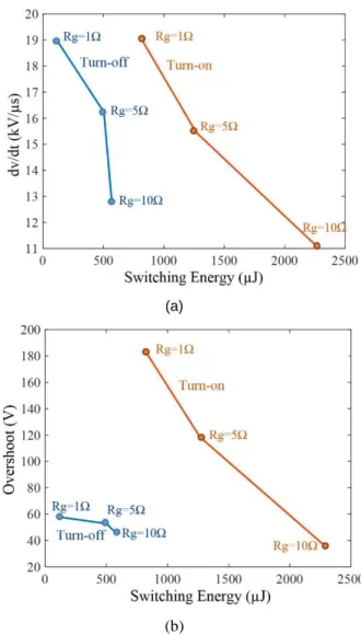
Fig. 2. Developed test board used for switching characteristics measurements
We applied this method in a test bench used for measurement of switching characteristics. A test board, specifically designed to characterize the CAS100H12AM1 SiC module, is presented in Fig. 2. This bench is used to build a mapping of switching losses, switching speed (4 /4 ) and also overshoot versus DC bus voltage 54 , line current 6 and driver parameters (gate-source voltage 57", gate resistance
7 and dead time 8).
(a)
(b)
Fig. 3. Relationship between switching energies and (a) switching speed and (b) overshoot, for different
Rg, at Vdc = 540V and Iinverter = 50A.
As an example of results, Fig. 3-a shows the relationship between switching energies (at turn-on and turn-off), 4 /4 and gate resistance at 50 , for a DC bus voltage of 5405 and 57" = 205. The same is shown in Fig. 3-b, but related to the overshoot during commutation.
The characterization results show that the higher the 7, the lower both overshoot and switching speed 4 /4 but the higher the switching losses. Note that, when changing Rg from 10Ω ! 1Ω, total energy (turn-on + turn-off) decreases from around 2850 ! 930 μC (3 times lower switching losses).
However, maximum 4 /4 and maximum overshoot increases 1.5 and 4 times, respectively.
In the next session we use these experimental data and the developed propagation model to study the impact of fast switching on the harness output overvoltage.
4.
OVERVOLTAGEA
NALYSIS BY SIMULATION:
TRAPEZOIDAL APPROXIMATION OF
S
IC
INVERTER WAVEFORM
Overvoltage at motor’s terminals is strongly related to harness length and also to inverter waveform 4 /4 (controlled by 7 in our case). In the following, we propose a parametric study of the overvoltage as a function of these two parameters. The results presented below use RLCG harness parameters calculated by the Finite Element Method (FEM) using FEMM software. The harness consists of two parallel AWG18 aeronautical cables (EN2267– 010A). For simplicity we represent the motor by a constant resistance equal to : ./0/1= 5000D. The inverter is often approximated to a trapezoidal source voltage (the inverter internal impedance
EFGH10H1 is neglected). Fig. 5 shows an example of
the rising edge of a trapezoidal voltage waveform at the output of a converter. The 4 /4 of each curve corresponds to that measured during the SiC MOSFET characterization (Fig. 3), for three different Rg (1, 5 and 10Ω).
Fig. 4. General synoptic of proposed overvoltage calculation algorithm
The developed algorithm shown in Fig. 4 is used to calculate the voltage waveform at motor terminals caused by trapezoidal inverter waveforms (Fig. 5). Results are shown in Fig. 6 and Fig. 7.
Fig. 5. Trapezoidal approximation of SiC inverter output waveforms for different Rg, at Vdc = 540V
and inverter output current Iinverter = 50A.
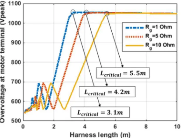
For a given inverter voltage waveform, the maximal overvoltage increases with respect to the harness length. Its maximum value is achieved at the so called critical cable length (Fig. 7). For harness lengths greater than the critical cable length, the overvoltage value decreases slightly as a function of harness length due to losses. But it remains fairly close to 2p.u. (Fig. 6 and Fig. 7).
For this studied case (overvoltage following a single edge), it is important to emphasize that the maximum value of the overvoltage does not exceed 2p.u. (2 times DC bus voltage: 1080V).
Fig. 6. Overvoltage at motor terminals obtained by simulation using trapezoidal inverter waveforms
(Fig. 5) for different 7 at = 3I.
The overvoltage results obtained with trapezoidal waveforms (Fig. 7) are similar to the trends proposed in the EIC standard 60034-18-41.
The adopted frequency approach allowed us to reproduce results well known in the literature in a very simple and extremely rapid way (few seconds) and with a better numerical accuracy.
ELECTRIMACS 2017, 4th -6th July 2017, Toulouse, France
The trapezoidal waveform hypothesis considers the inverter as a perfect voltage source: in other words the dynamics of its output voltage is not affected by the inverter’s load (harness + motor). Of course, this approach is not extremely rigorous, nevertheless it allows us to highlight that increasing the Jis potentially a very simple solution which would significantly reduce motor overvoltage for relatively small harness lengths; in aircraft applications, the length of the harness varies from a few centimeters to a few tenths of meters. The drawback of increasing Rg is that switching losses also increase (Section 3). Therefore, to ensure at same time better inverter energy efficiency and the EIS reliability, a trade-off between losses and transient overvoltage must be considered right from the design step.
Fig. 7. Maximal overvoltage at motor terminals for different harness lengths, obtained by simulation
using trapezoidal inverter waveforms. 5.
O
VERVOLTAGE VS.
S
IC
INVERTER EXPERIMENTAL VOLTAGE WAVEFORMThe fast switching of a SiC inverter generates very complex resonance phenomena. The output inverter waveform cannot be actually considered as a trapezoidal waveform such as the ones of Fig. 5. The experimental shapes depend on several parameters, mainly on the power modules parasitics (loop inductance, semiconductor output capacitance) but also the output current and the DC voltage. In the measurements presented below, voltage waveforms present ringing phenomena at 25MHz just after each commutation.
To study the impact of SiC inverter voltage waveform on transient overvoltage, we carried out experimental investigations using a two legs SiC inverter based on CMF20120D components connected to a two parallel aeronautical cables (AWG18–EN2267–010A). No load is connected, which is a worst case in terms of reflection on the load side. The three studied cases are:
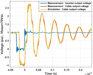
• Case 1 – Overvoltage caused by a single rising edge (Fig. 8).
• Case 2 – Overvoltage caused by an inverter voltage falling front edge followed by a rising one (Fig. 9)
• Case 3 – Overvoltage caused by resonance between inverter and harness (Fig. 10). For the two first cases (1 and 2) a long cable of 18.7m is used, which causes a harness oscillation frequency (around 2.25MHz) much lower than the characteristic voltage inverter ringing frequency (around 25MHz). Therefore, the two transient phenomena caused by SiC inverter and cable are relatively decoupled. Under the trapezoidal waveform assumption (as shown in the previous section), overvoltage has been shown to remain under 2p.u. However, as clearly demonstrated by experimental test and simulation (Fig. 8), overvoltage caused by single rising edge are greater than 2p.u. In fact the overvoltage caused by the inverter is superposed with that generated by the cable.
We emphasize here the noticeable agreement between experimental and simulated waveforms during the first voltage pulse.
Case 2 is conventionally classified as overvoltage greater than 2p.u.[3]. Indeed, supplying a harness by a falling edge generates at its output an overvoltage which varies between (-1p.u. and 1p.u.). A rising edge generates an overvoltage between (0p.u. and 2p.u.). If those two edges are sufficiently close together (depending on pulse duration) they can either be subtracted or added (Fig. 9). In the worst scenario (addition), the overvoltage can reach 3p.u.
Case 3 uses a relatively short cable of 2.3m. At this length, the cable presents a resonance frequency close to the ringing frequency at the output of the inverter. A dangerous resonance is observed (Fig. 10), caused by interaction between the inverter overvoltage and that of the cable, and it gives rise to an overvoltage greater than 3p.u. in our case. To our knowledge, this new result is original and was never addressed in the literature before.
Fig. 8. Overvoltage caused by a single rising edge for Vdc=70V, Rg=10Ω, Vgs=24V and cable
Fig. 9. Overvoltage caused by a falling edge followed by a rising one for Vdc=70V, Rg=10Ω,
Vgs=24V and cable length=18.7m.
Fig. 10. Overvoltage caused by resonance between inverter and harness for Vdc=70V, Rg=10Ω,
Vgs=24V and cable length=2.3m.
For the three studied cases, by using the measured inverter voltage, our model is able to reproduce with very good precision the harness output overvoltage. The prediction error of the maximum voltage is less than 7%.
The inaccuracy in the critical case 3 is due to the fact that the interactions between the inverter and the harness are not rigorously taken into account. Indeed the voltage of the inverter is based on measurements and imposed at the input of the cable.
The simulation results show the relevance of the proposed harness model. Future works aim to build sophisticated inverter and motor models to rigorously simulate the different interactions in electromechanical chain.
6. C
ONCLUSIONIn this paper we propose a propagation frequency model providing fast and accurate simulation of overvoltage along the harness.
Using this model and the experimental characterizations of a SiC inverter, a parametric study of the overvoltage at motor terminals versus SiC gate resistance J and harness length is presented. We also show that the variation of the gate resistance
J could be used to mitigate motor overvoltage in applications with small cable length values (as in some aeronautical applications).
Experimental and simulation investigations allow to identify the harmful effects of the voltage ringing at the output of the SiC inverter, which create very high voltage resonances capable to destroy the electromechanical EIS.
R
EFERENCE[1] X. Roboam, “New trends and challenges of electrical networks embedded in ‘more electrical aircraft,’” in 2011 IEEE International Symposium on Industrial Electronics, 2011, pp. 26–31.
[2] P. Bidan, T. Lebey, and C. Neacsu, “Development of a new off-line test procedure for low voltage rotating machines fed by adjustable speed drives (ASD),” IEEE Trans. Dielectr. Electr. Insul., vol. 10, no. 1, pp. 168–175, 2003.
[3] G. Skibinski, R. Kerkman, D. Leggate, J. Pankau, and D. Schlegel, “Reflected wave modeling techniques for PWM AC motor drives,” APEC ’98 Thirteen. Annu. Appl. Power Electron. Conf. Expo., vol. 2, pp. 1021–1029, 1998.
[4] S. Amarir and K. Al-Haddad, “Over-voltages computation algorithm for motors fed from long cable PWM drives,” Proc. Mediterr. Electrotech. Conf. - MELECON, pp. 554– 559, 2008.
[5] G. Metzger and J.-P. Vabre, Électronique des impulsions. Paris, 1966.
[6] C. R. Paul, Analysis of multiconductor transmission lines, 2nd ed. 2008.
[7] F. Krismer and J. W. Kolar, “Accurate Power Loss Model Derivation of a High-Current Dual Active Bridge Converter for an Automotive Application,” IEEE Trans. Ind. Electron., vol. 57, no. 3, pp. 881–891, Mar. 2010.
[8] B. Cougo, H. Schneider, T. Meynard “Accurate switching energy estimation of wide bandgap devices used in converters for aircraft applications,” in 15th European Conference on Power Electronics and Applications (EPE), 2013.