HAL Id: hal-03002987
https://hal.archives-ouvertes.fr/hal-03002987
Submitted on 13 Nov 2020
HAL is a multi-disciplinary open access archive for the deposit and dissemination of sci-entific research documents, whether they are pub-lished or not. The documents may come from teaching and research institutions in France or abroad, or from public or private research centers.
L’archive ouverte pluridisciplinaire HAL, est destinée au dépôt et à la diffusion de documents scientifiques de niveau recherche, publiés ou non, émanant des établissements d’enseignement et de recherche français ou étrangers, des laboratoires publics ou privés.
Space charge characterization in insulating materials
used in aircraft cables
Amin Benyoucef, Laurent Berquez, G. Teyssedre, Eddy Aubert
To cite this version:
Amin Benyoucef, Laurent Berquez, G. Teyssedre, Eddy Aubert. Space charge characterization in insulating materials used in aircraft cables. Internat. Conf. on High Voltage Engineering (ICHVE), Beijing, China, 6-10 Sept. 2020, Sep 2020, Beijing, China. pp. 351-354. �hal-03002987�
Space Charge Characterization in Insulating
Materials used in Aircraft Cables
Amin Benyoucef
Laplace, Paul Sabatier University and IRT Saint Exupery
Toulouse, France [email protected]
Gilbert Teyssedre
Laplace, Paul Sabatier University
Toulouse, France
Laurent Berquez
Laplace, Paul Sabatier University
Toulouse, France
[email protected] Eddy Aubert
IRT Saint Exupery, and Safran Electric and Power
Toulouse / Blagnac, France [email protected]
Abstract— The increase of on-board power in aircrafts will
probably go with massive introduction of DC networks. Though voltages are much less than in power transmission cables, weight optimization implies that systems are not overdesigned. Besides, aeronautic specifications and environment stresses are more demanding. One popular cable technology uses wrapped insulation, with polyimide (PI) as inner insulation and polytetrafluoroethylene (PTFE) as outer layers, ensuring fire resistance and arc tracking resistance properties. Space charge measurements in such multilayer is more complex than in extruded cables. In order to anticipate issues with direct measurements on cables, multilayers of PI and PTFE have been investigated by pulsed electroacoustic (PEA) method. For PI, we clearly show that the fluorinated layer added onto PI to improve adhesion between rolls has a strong impact on the response. The PEA signal is influenced by the bilayer formed due to dielectric permittivity difference mainly. When associating PTFE and PI, the charge resolution within PI is further distorted due to the strong diffusivity of PTFE for acoustic waves. From the present results, difficulties forecasted for the measurement on cable materials are discussed.
Keywords—DC technologies, aeronautic cables, PEA method, space charges
I. INTRODUCTION
Whereas in the field of power transmission high voltage means several hundreds of kV, in aerospace application it can be just some hundreds of volts. Yet, because of the severe environment and specifications required for power systems of aircraft, increasing power is far from being a simple task, as it has to be achieved in a constrained space with optimization requirements in terms of weight. In this context, HVDC tends to be introduced on aircraft networks, just because it could decrease losses and global weight of electrical equipment. For example, the reduction of skin effects for conductor would go with a decrease in losses in cables when switching from 400 Hz HVAC network to DC. This switch from AC to DC goes with safer operation conditions regarding partial discharges effects. However, it brings to questioning about new potential risks introduced for aircraft Electrical Wiring Interconnection System (EWIS) reliability.
Like when developing synthetic insulation for DC transmission energy, space charge phenomena and associated electric field redistribution are addressed. Though voltages are much less than in energy transmission network, cable
structure and insulation process are more complex, making space charge measurements not a routine task. Indeed, in the aircraft cable technology considered here, the insulation is made of wrapped polyimide (PI) and polytetrafluoroethylene (PTFE) multilayers, see Fig. 1. Here the PTFE is made with 100 µm thick tapes. The PI film is provided with noticeable fluorinated layers at both sides to improve adhesion.
Space charge measurements on multilayers are not new. Measurements on bi-layers with cable insulation / joint insulation have been investigated [1] [2] along with multilayers of paper /oil insulations [3]. However, in these cases, the thickness of the various layers was adapted to fit to the measurement method, which is not feasible with tapes used here. Besides, in these simple cases, not all the contributions to the acoustic signal are necessarily treated.
In order to anticipate issues for space charge measurements on real cables, preliminary space charge measurements by Pulsed Electro-Acoustic (PEA) method were achieved on flat samples.
II. EXPERIMENTAL METHODS A. Materials
Polyimide (PI) films were provided in the form of film with 50 µm of pure Kapton-HN film, associated with fluorinated polymer layers (being fluorinated ethylene-propylene copolymer –FEP). Such films will be called PI+F in the following. Polytetrafluoroethylene (PTFE) samples were provided un-sintered, with 100 µm thickness. They were processed as to form bilayers, of the same material for
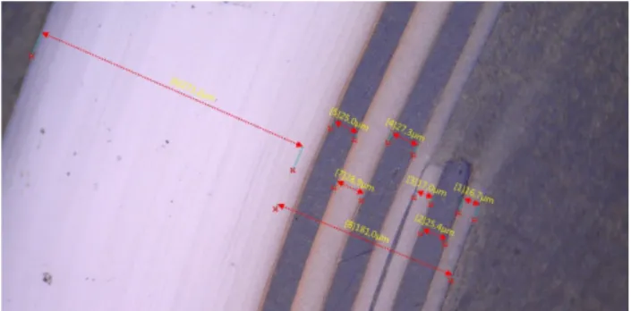
Fig. 1 Example of cross-section of a aeronautic cable with wrapped insulation of about 450 µm thickness. The PTFE insulation (left) is 270 µm thick. PI (dark) tapes are 25 µm thick.
reaching a thickness compatible with PEA test cell requirements or of different materials as to reproduce the wrapping process used in cable insulation processing. The sintering of PTFE single films (with final thickness about 75 µm), or combined with PI+F film was achieved at 360°C for 10 min under hot press.
B. PEA tests
A Standard PEA test cell for flat specimen was used, with Aluminium as ground electrode and semiconducting material as top electrode. The PEA cell is from FiveLab, Japan, with good performances for thin samples. We present data obtained at room temperature under low DC field up to 3 kV/mm to discuss signal quality. In all of the results presented here, the signal due to pulsed voltage only (≈150 V applied taking into account losses in matching circuit) is subtracted.
III. RESULTS AND DISCUSSIONS A. Acoustic signal generation
The general equation governing acoustic signal of a dielectric layer submitted to homogeneous pulse field δE#, at
1st order is the following [1] [4]:
δ𝑓% = ρδ𝐸#− 𝐸+,
∂(ϵ + γ) ∂𝑥 δ𝐸#− 𝛾
∂𝐸+,
∂𝑥 δ𝐸# (1)
where fs is the force density (N/m³), ε the dielectric
permittivity, γ the electrostriction coefficient, EDC the static
field, ρ the charge density. In presence of materials of different permittivities, even without internal charges, the second term in Eq. [1] leads to a pressure generation of the form:
δ𝑝% = −𝐷
ϵ7− ϵ8
ϵ7 δ𝐸# (2)
Here D is the electric displacement. The signal depends on the fate of acoustic waves along their way to the sensor. Attenuation and dispersion of waves are accounted for as well as reflexions occurring at the interface between two materials due to acoustic impedance mismatch. The main quantities related to the materials used here are listed in Table 1.
TABLE I. PROPERTIES OF INVESTIGATED MATERIALS
Propertya PTFE +F PI Relative permittivity 2.1 2.05 b 3.4 Conductivité (S/m) 10-16 10-15 b 7×10-16 Acoustic Impedance (kg.m-2.s-1) 2.90×10⁶ 2.80×10⁶ 3.12×10⁶ Specific weight (kg/m³) 2200 2150 b 1420 Sound velocity (m/s) 1310 c 1300 d 2200 a.At room temperature b Dupont FEP datasheet c from [5] d from [6]
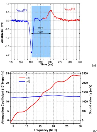
For calibrating signal and treating the distortion of acoustic waves during transit, a known charge amount is usually set onto the top and bottom electrodes. In the case of bi-layers the procedure becomes more complicated because of perturbation of the propagating waves by two materials plus interface. To reach the required quantities, layers were taken separately. For PTFE, which is known as a strongly diffusing material, the acoustic signal obtained under 500 V DC voltage is plotted in Fig. 2a. The spectra for acoustic attenuation and sound velocity (Fig. 2b) were deduced from [7]:
α(𝑓) =−1 𝑑 𝑙𝑛 > 𝑉#@A8(𝑓) 𝑉#@A7(𝑓)> 𝑐(𝑓) = 2. 𝜋. 𝑓. 𝑑 φ G𝑉#@A7(𝑓)H − φ G𝑉#@A8(𝑓)H (3)
where d is the dielectric thickness and Vpeak (f) is the Fourier
transform of rough acoustic signal.
Repeating the procedure for PI material was not as a straightforward case as expected. Fig. 3 shows the calibration signal obtained for the PI+F film, with inversion of the film in the PEA cell. An internal charge peak is clearly visible into the material, at about 6 ns from the interface peak, the time between electrode/insulation interface peaks being about 30 ns. Looking at the scanning electron microscope and optical microscope images given in Fig. 4, it is obvious that the films are effectively made of a main PI layer of about 50 µm in thickness and a surface layer that is revealed as FEP, apparently assembled by an adhesion layer. In these
(a)
(b) Fig. 2 Calibration signal (a) obtained on a 75 µm thick PTFE film using a DC voltage of 500 V and deduced attenuation and velocity spectra (b).
Fig. 3 Calibration signal for ≈70 µm thick 'PI+F' film considering reversing of the sample in respect to the electrodes. DC voltage= 180 V.
5 10 15 20 25 30 0 5 10 15 20 25 0 500 1000 1500 2000 2500 a(f) A tt enu at ion C oef fi ci ent ( 10 3 N ep er /m ) Frequency (MHz) c(f) Sou nd v el oci ty ( m/ s) 120 150 180 210 240 270 300 330 -8 -4 0 4 8 Front Back Am pli tud e (mV ) Time (ns)
conditions, reliable acoustic signal for calibration purpose could not be obtained from these PI films.
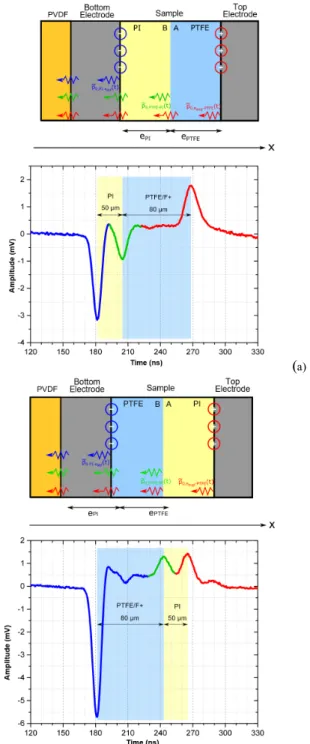
B. Measurements on bi-layers
Figure 5 depicts the rough PEA signals obtained on a PI+F/PTFE sample using an applied voltage of 1100 V. The layers are the same as probed in section A. One interface peak is clearly revealed on the profiles. According to Fig. 5a, it is localized at about 26 ns from the surface of the PI layer.
The sound velocity in PTFE is substantially less (1310 m/s) than in other insulating materials [5], consistently with its relatively soft mechanical response, as compared to 2200 m/s for PI. Consequently, the geometrical distribution of the layers is not reflected in the acoustic response in time. Comparing this signal to the response of the single PI+F layer, it seems that the interface being detected in Fig. 5 is that between the PI and the +F layer. It can be reasonably assumed that the +F layer is stick to PTFE and that the interface between +F layer and PTFE does not produce specific signal. This is consistent with the results given in Table 1. Indeed, the acoustic impedances of PTFE and +F are similar; the permittivity of the two materials are similar, and therefore as far as short stressing time is considered, there is no reason to have electro-acoustic activity at this interface. The situation may possibly change with time as the conductivity of fluorinated layer and PTFE are presumably not the same (only rough values for FEP issued from datasheets are given in Table 1), such that interface charging may be at play.
The sign of the acoustic signal from the PI+F/PTFE interface is the same as that of the PI+F electrode interface. Reasoning on the field distribution, this is an expected behaviour as the permittivity in PTFE is less than in PI, hence the field should be moved to PTFE, and a charge assimilated to an homocharge viewed from the electrode on the PI side should appear. However, the scheme is not necessarily so obvious as the pressure at the interface is generated by the field difference and not by charges. Let consider Eq. 2 applied to idealized bi-layer.
The following set of equations can be deduced for respectively the pressure generated at the electrode/PI interface, the PI+F/PTFE interface and at the PTFE/electrode interface: 𝑝IJ,LM@NOP(𝑡) = − εL. εS8 (𝑒S. εL+ 𝑒L. εS)8. 𝑉+,. 𝑣#(𝑡) (4) 𝑝IJ,SML(𝑡) = εS8. εL8 (𝑒S. εL+ 𝑒L. εS)8. V 1 εL− 1 εSW . 𝑉+,. 𝑣#(𝑡) (5) 𝑝IJ,@XYZMS(𝑡) = εS. εL8 (𝑒S. εL+ 𝑒L. εS)8. 𝑉+,. 𝑣#(𝑡) (6)
Table 2 provides the pressure at each interface, taking into account the reflexion at the internal interface (TAB≈1.04 and
0.96 for Fig. 5a and 5b) and the attenuation coefficient of the PTFE layer: it was deduced as 75% at the main peak frequency (19 MHz) considering α(f) of Fig. 2 and a thickness of 80 µm. The attenuation in PI was neglected. The results are grossly consistent with measured signals. The interface charge measured at the PTFE/electrode interface is larger than at the PI side, and the attenuation explains changes when reversing sample. The measured acoustic signal at dielectric/dielectric interface is slightly lower than expected considering solely the field contribution (Fig. 5a).
TABLE II. PRESSURE AMPLITUDES OBTAINED FROM EQ.(4-6) Fig. 4 Optical (left) and SEM images of 'PI' film cross-section.
(a)
(b) Fig. 5 PEA signal for 2 orientations of the PTFE/PI+F sample in the PEA cell. Applied DC voltage: 1100V.
P (Pa) for: Electrode Lower A-B Electrode Upper
Fig. 5a -587 -347 933
Fig. 5a-corr a -587 -347 243
Fig. 5b-corr a -933 87 141
a Pressure corrected for absorption in PTFE and for reflection at PI/PTFE-F+ interface
C. Measurements on multi-layers
In order to investigate space charge behaviour in wrapped PI, several layers of the same material (with +F layer on one face) were piled up and tested by PEA. Materials were assembled under hot press in the same way as previously. Fig. 6 shows the obtained result with reversing the sample in the cell. Multiple peaks occur in the sample thickness due to the superposition of layers of various materials. Besides, along with acoustic waves generation due to field step, there may be reflection of waves that makes the response further complex. In multilayer PTFE, no signal was detected at the interfaces between layers. There can however be several reasons for signal generation, or propagation perturbation as discussed by Mier et al [8] such as non- uniform thickness of the built sample, or polarization due surface pollution/oxidation. Holé et al analysed the impact of material loading with particles of various size on the significance of rough signal for different methods [9]. With uniformly distributed particles of size smaller than the resolution, the response of the material can be considered as if it is homogeneous. When dealing with impregnated paper insulation, or alternated oil/impregnated paper, relatively thick layers, typically 70 µm are used [3]. Echigo et al reported on space charges in 5-layers stratified PCB made of aramid paper and epoxy resin, with about 100 µm thickness for each layer [10]. In these cases, the electrode signals were clear enough to allow calibration. In the situation of Fig. 6, the dielectric is made of layers thicker than the resolution, but not thick enough to fully resolve signal from interfaces. In these conditions it become extremely difficult to extract charge profiles in the multilayer. Only making the resolution extremely coarse could hide the problem, but the significance would be questioned.
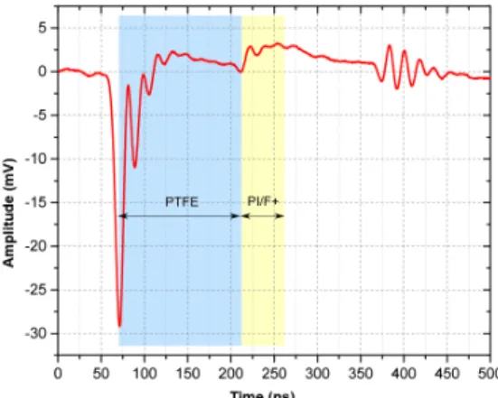
Space charges in cables can however be investigated. Fig. 7 shows the signal obtained from the cable with cross-section of Fig. 1. The oscillations near the ground electrode are due to impedance mismatch of the pulse generator/cable and not to material response. All the signal from the PI layers is smeared out into a broad peak, because of diffusion by the PTFE layer before detection of acoustic signal. In spite of that, the part of the signal corresponding to the PTFE layer can be exploited [11].
IV. CONCLUSION
The structure of aeronautic cables makes it not an easy task to probe it for space charge build-up. The global PTFE/PI/fluorinated polymer multi-layer structure could be analysed with distinguishing space charge effect from permittivity step effects in the acoustic signal. However, the PI film is composed of layers of PI and of fluorinated polymer, about 10 µm in thickness, i.e. of the same order as the resolution of the PEA cell. When such layer is in contact with the electrode, spurious signal is detected. In a cable, the PTFE layer, which is at outer part of the cable, is in contact with the detection cell, and substantially broadens the signal issued from the PI layers. Therefore, space charge measurements in cables having such structure can be analysed from the PTFE
side only, with indirect effects linked to charge build-up in PI at the interface.
REFERENCES
[1] R. Bodega, P.H.F. Morshuis and J.J. Smit "Space charge measurements on multi-dielectrics by means of the Pulsed Electro Acoustic method", IEEE Trans. Dielectr. Electr. Insul., vol. 13, pp. 272-281, 2006. [2] T.T.N. Vu, G. Teyssedre, B. Vissouvanadin, S. Le Roy, and C. Laurent,
"Correlating conductivity and space charge measurements in multi-dielectrics under various electrical and thermal stresses", IEEE Trans. Dielectr. Electr. Insul., vol. 22, pp. 117-127, 2015.
[3] J. Hao, G. Chen, R.J. Liao, L.J. Yang, and C. Tang, "Influence of moisture on space charge dynamics in multilayer oil-paper insulation, IEEE Trans. Dielectr. Electr. Insul., vol. 19, pp. 1456–1464, 2012. [4] S. Holé, T. Ditchi, and J. Lewiner, "Influence of divergent electric
fields on space-charge distribution measurements by elastic methods," Phys. Rev. B, vol. 61, pp. 13528–13539, 2000.
[5] P.J. Rae and E.N. Brown, "Some observations on measuring sound speeds in polymers using time-of-flight", Experimental Techniques, vol. 40, pp. 1085–1097, 2016.
[6] G.M. Sessler, C. Alquié, and J. Lewiner, "Charge distribution in Teflon FEP (fluoroethylenepropylene) negatively corona‐charged to high potentials", J. Appl. Phys, vol. 71, pp. 2280-2284, 1992.
[7] T. Ditchi, C. Alquié, and J. Lewiner, “Broadband determination of ultrasonic attenuation and phase velocity in insulating materials,” J. Acoust. Soc. Am, vol. 94, pp. 3061–3065, 1993.
[8] G. Mier-Escurra, A. Rodrigo-Mor, and P. Vaessen, "A calibration method for acoustic space charge measurements using multilayer samples", Sensors, vol.18, p.2508, 2018.
[9] S. Holé, A. Sylvestre, O. Gallot Lavallée, C. Guillermin, P. Rain, and S. Rowe, "Space charge distribution measurement methods and particle loaded insulating materials", J. Phys. D: Appl. Phys., vol. 39, pp. 950– 956, 2006.
Fig. 6 Rough acoustic signals obtained on two layers of PI+F with inversing the sample in the cell. Applied DC voltage of 390 V. Total thickness is 130µm.
Fig. 7 PEA signal under -9 kV DC voltage for a cable with geometry shown in Fig. 1. 120 150 180 210 240 270 300 330 -6 -4 -2 0 2 4 6 Front Back A mp li tu de ( m V ) Time (ns)
[10] Y. Echigo, H. Tanaka, Y. Ohki, K. Fukunaga, T. Maeno and K. Okamoto, "Effects of humidity and temperature on space charge distribution profiles in printed circuit board insulations," Proc. 2007 IEEE-ICSD, Winchester, pp. 458-461, 2007.
[11] A. Benyoucef, L. Berquez, G. Teyssedre, and E. Aubert, "Space charge measurement by PEA on an aeronautical cable ", Proc. IEEE Internat. Conf. on Dielectrics (ICD), Valencia, Spain, 5-9 July 2020.