HAL Id: hal-02390966
https://hal.archives-ouvertes.fr/hal-02390966
Submitted on 1 Dec 2020
HAL is a multi-disciplinary open access
archive for the deposit and dissemination of
sci-entific research documents, whether they are
pub-lished or not. The documents may come from
teaching and research institutions in France or
abroad, or from public or private research centers.
L’archive ouverte pluridisciplinaire HAL, est
destinée au dépôt et à la diffusion de documents
scientifiques de niveau recherche, publiés ou non,
émanant des établissements d’enseignement et de
recherche français ou étrangers, des laboratoires
publics ou privés.
flying capacitor cells
Frederico Matos, Marcos Mendes, Thierry Meynard, Victor Mendes
To cite this version:
Frederico Matos, Marcos Mendes, Thierry Meynard, Victor Mendes. A generalized open-end
wind-ing conversion system uswind-ing flywind-ing capacitor cells. Electric Power Systems Research, Elsevier, 2019,
�10.1016/j.epsr.2018.12.024�. �hal-02390966�
Contents lists available atScienceDirect
Electric Power Systems Research
journal homepage:www.elsevier.com/locate/epsr
A generalized open-end winding conversion system using
flying capacitor
cells
Frederico F.V. Matos
a,⁎, Marcos A.S. Mendes
a, Thierry Meynard
b, Victor F. Mendes
aaGraduate Program in Electrical Engineering, Federal University of Minas Gerais, Av. Antonio Carlos, 6627, 31270-901 Belo Horizonte, Brazil bPlasma and Energy Conversion Laboratory, Institut National Polytechnique de Toulouse 2, rue Charles Camichel, 31071 Toulouse, France
A R T I C L E I N F O Keywords:
Multilevel systems
Pulse width modulated power converters Power conversion
Flying capacitor converters Open-end winding
A B S T R A C T
Over the years, industrial processes, renewable energy systems and electrification of transport systems have been pushing power electronics equipment towards higher power ratings, quality and faster dynamics. In this context, several multilevel converter structures were developed and became popular, such as neutral-point-clamped, flying capacitor and cascaded half-bridge. This paper presents a generalized n-level converter using the multicell flying capacitor structure in an open-end winding configuration. A mathematical analysis shows that the pro-posed system presents the same output voltages as a traditionalΔ/Y structure, but with less energy storage in the flying capacitors. The correlation with the traditional structure allows the use of an optimized modulation technique developed for theflying capacitor converter. It results in a voltage output with optimized harmonics, keeps the losses evenly distributed among the switching devices, and balances the voltages in theflying capa-citors. Experimental results from a three-level conversion system and simulation results from a five-level structure demonstrate the features of the proposed topology.
1. Introduction
Over the last decades, several multilevel converter topologies were developed in order to achieve superior power, energy quality or dy-namics over the traditional two level structure. Generally, they consist in different forms of connection between the switching devices and capacitive elements, producing multiple voltage steps at the converter output. A significant variety of topologies exist, each one with specific characteristics: number and ratings of switches, capacitors, necessity of isolated supplies, modularity, etc. The authors bring in[1], along with their own proposed topology, a comparison of several structures re-garding the number of switches and capacitors. The neutral point clamped (NPC), flying capacitor (FC) and cascaded H-bridge (CHB), nevertheless, were the ones that achieved higher acceptance and be-came widely known[2].
Another form of producing multilevel voltages in a drive system is the open-end winding (OEW) connection, first presented by Guggenbach and Stemmler in 1993[3]and illustrated inFig. 1. In this configuration, the load is not Y or Δ connected; instead, each side of the windings is fed by a converter. These can either be two-level or mul-tilevel converters such as NPC or FC. At the grid side, a transformer isolates the two converters in order to avoid the circulation of common-mode currents through the circuit. One of the main advantages of this structure is the lower device count compared to a traditional Δ/Y
system with the same topology and number of levels. An OEW drive using dual three-level NPC converters, for example, presents the same voltage levels than a traditionalfive-level NPC, uses the same number of active switches, but less clamping diodes.
OEW structures have been reported for various applications, such as electrical and hybrid vehicles[4], aerospace[5], water pumping solar systems[6,7]and wind power[8,9], to name a few. Also, the combi-nation of power converters with different number of levels[10,11]and topologies[12–14]have been proposed.
Along with the variety of structures, several modulation techniques were developed specifically for OEW systems, as the sub-hexagon strategies in [15–17], the carrier based in [18–20]and those with predefined switching sequences in[21,22]. Most of these techniques, however, propose an alternating role between the converters: while one of them is effectively switched, the other one is clamped at a certain switching state. With those strategies, the current ripple has the fre-quency of the converter switching, making them less attractive for high power devices, that switch at low frequencies. Some strategies are particular for a specific converter configuration, not being easy to be adapted for a different number of levels. Others lead to a poor dis-tribution of losses between the switches, which can affect the converter life-time.
In this work, a generalized n-level OEW structure that employs flying capacitor cells is presented. It features some important
https://doi.org/10.1016/j.epsr.2018.12.024
Received 3 August 2018; Received in revised form 27 November 2018; Accepted 25 December 2018
⁎Corresponding author.
Electric Power Systems Research 169 (2019) 174–183
Available online 09 January 2019
0378-7796/ © 2018 Elsevier B.V. All rights reserved.
advantages:
•
with FC multicell construction, increasing the voltage and/or the number of output levels is easily achievable by increasing the number of power cells;•
all switching devices (of both converters) present the same blocking voltage, which is a fraction of the voltage applied at the output;•
the total required energy storage of the flying capacitors is sig-nificantly lower than that of a traditional Δ/Y system;•
it employs the centered space vector pulse width modulation (CSVPWM) with state machine decoder[23,24], that lead to optimal harmonic content with an even distribution of losses among the devices, and is easily adaptable to different number of output levels. Rather than the system proposition itself, which is formed by the combination of the well known FC and OEW technologies, the main contribution of this paper is the original mathematical description that correlates an OEW and a traditional multilevel structure: it is shown that, by directing the command signals to the proper devices in the OEW topology, the voltage output is exactly the same as it would be in a Δ/Y connected system, independently on the number of levels. This important observation makes it possible to the presented OEW structure to use optimized modulation techniques originally developed for tra-ditional FC drives, such as the CSVPWM with state machine decoder.Besides that, a novel analytical comparison of the energy stored in the flying capacitors is presented, concluding that the multilevel FC configuration in an OEW fashion demands less storage than the corre-spondingΔ/Y system.
The development of these mathematical expressions are presented in Section2. In Section3, the CSVPWM with state machine decoder is described. Finally, Sections4and5present simulation results of a five-level structure and experimental results from a 2 kW test bench in a three-level configuration, respectively, demonstrating the features and feasibility of the structure.
2. System modeling
In this section, the output voltage equations of the proposed OEW system is presented as a function of the switching command signals. First, the analysis is developed for a three-level system, comparing the OEW structure with a traditional FC converter in order to show the equivalence between both topologies. Then, the system is generalized for a n-level OEW structure. Finally, a mathematical analysis of the energy stored in theflying capacitors evidences its important reduction on the OEW system compared to the traditional structure.
2.1. The three-level converter
The analysis begins by resuming the voltage equations of the tra-ditional three-levelflying capacitor, shown inFig. 2. The DC-link and theflying capacitors are charged with a v /2dc voltage and the load is an equilibrated impedance (Za= Zb= Zc). n′ is the DC-link midpoint and n
is the common point of the star-connected load. The command signals of the top switching devices are Sxj⊂ {1, 0}, and for the bottom
switches the complementaryS¯xj, where x⊂ {a, b, c} and j ⊂ {1, 2}. The equations for the phase voltages in this system are
= − = − = − ′ ′ ′ ′ ′ ′ v v v v v v v v v an an nn bn bn nn cn cn nn (1)
The converter output voltage for any of the phases,vxn′, can be written as a function of their respective command signals and the DC-link voltage: = − + + ′ v v v S S 2 2 ( x x) xn dc dc 1 2 (2)
From(2)it can be seen that the output voltage can assume three different levels (0V, ± v /2dc ), with two redundant switching states producing the zero value.
Once the points n and n′ are isolated, there is no path for circulation of zero-sequence currents. The voltagevnn′can, then, be expressed as
= + + ′ ′ ′ ′ v v v v 3 nn an bn cn (3) Now, a similar analysis is carried out for the three-level OEW drive shown inFig. 3. The winding voltages equations are
= − − = − − = − − ′ ′ ′ ′ ′ ′ ′ ′ ′ ′ ′ ′ v v v v v v v v v v v v a o o o b o o o c o o o aa ao bb bo cc co (4)
The individual output voltages of the converters are
= − + = − ′ ′ v v v S v v v S /4 /2( ) /4 /2( ) x x o x xo dc dc 1 dc dc 2 (5)
and their subtraction leads to the total output voltage
= − ′ ′= − + +
v v v v v S S
2 2 ( )
x o x x
outx xo dc dc 1 2 (6)
Considering that there is no connection between points o and o′, no common-mode currents circulate in this system. Thus, the voltagevo o′ can be written as = − + − + − ′ ′ ′ ′ ′ ′ ′
(
)
(
)
(
)
v v v v v v v 3 o o ao a o bo b o co c o (7) A direct comparison shows that(6)=(2), i.e.vxo−vx o′ ′=vxn′. That is achieved by directing the Sx1command signals to the TOP switches ofconverter 1 and the Sx2signals to the BOTTOM switches of converter 2
in the OEW structure, as depicted inFig. 3.
That way,vo o′ =vnn′((7)=(3)) and, therefore, it is possible to note that both topologies produce the same voltage pattern(4)=(1). This observation leads to the conclusion that modulation techniques
Fig. 1. Three-phase open end winding drive.
developed for three-level FC converters can be directly employed in a OEW system, leading to similar voltage waveforms.
2.2. An n-level converter
As the previous analysis showed the equivalence between three-level OEW drives and FC converters, this section presents the mathe-matical generalization for a n-level system. Fig. 4 shows the power structure for one phase of a generalized n-level multicell flying capa-citor converter. It is composed of (n− 1) = m power cells, and the kth
cell has a DC voltage of k m v( / ) dcacross itsflying capacitor. With such configuration, the blocking voltage of the semiconductor devices is
vdc/m[25].
The output voltage of such converter can be expressed as
∑
= − + ⎛ ⎝ ⎜ ⎞ ⎠ ⎟ = v v v m S 2 k m xo dc dc 1 xk (8) These FC cells can be employed in a three-phase OEW configuration, leading to the system presented inFig. 5. Converter 1 uses m1cells andconverter 2 uses m2cells per phase. The DC-link voltages are
propor-tional to the number of cells of each converter:
= ⎡ ⎣ ⎤⎦ = ⎡ ⎣ ⎤⎦ + + v v v v m m m m m m dc dc dc dc 1 1 1 2 2 2 1 2 (9)
The converters output voltages can be written as
(10) which lead to the output voltage expression
= − = − + ∑ + ∑ ′ ′ + = = ′ v v v S S ( ) x o v v m m k m k m x k out xo 2 1 xk 1 x dc dc 1 2 1 2 (11) By comparing(11) with(8), one can see the correlation between this OEW system and a traditional (Δ/Y) flying capacitor drive with (m1+ m2) cells. Both systems have the same number of switches, with
equal switching states redundancy and all switching devices have the same blocking voltage, which isvdc/(m1+m2)volts.
This is a very interesting feature, as it allows the OEW drive to use modulation techniques originally developed for FC converters. Section 3presents a modulation strategy that provides a voltage output with optimized harmonic distortion and evenly distribute the commutations between the switching devices in both FC and OEW systems.
2.3. Flying capacitors stored energy
One of the main advantages of the OEW configuration compared to the traditional one is presenting lower energy storage on the flying capacitors.
First, let's consider a traditionalΔ/Y system employing a FC con-verter with m cells. The capacitance of the flying capacitors is de-termined according to the admissible voltage ripple on the switching devicesΔvsw. Being Imax the maximum current and fswthe switching
frequency[25]: = C α I v f m Δ 1 fc max sw sw (12)
Theα variable is introduced to represent different conditions:
•
m = 1→ α = 0: No flying capacitors are employed (two-level con-verter);•
m = 2→ α = 1: There is one flying capacitor per phase. The DC-link, with its high capacitance value, normally presents a voltage ripple much lower than that of the FC. That being considered, we can assume thatΔvswcorresponds to the FC voltage ripple;•
m > 2→ α = 2: There are at least two flying capacitors per phase. In this case, a switching device placed between two FCs can be submitted to twice their voltage ripple. That is why the capacitance is doubled: to ensure that their ripple is lower thanΔvsw/2. The voltage in the kthcell isvk=( / )k m vdc, so the total stored energy in theflying capacitors is= ∑ = ∑ = − = −
(
)
W C v α k k m k I v f m v m k m fc 1 1 1 2 fc 2 1 2 Δ 1 1 1 2 max sw sw dc2 2 (13)Now let's assume the equivalent OEW structure, which employs dual converters of m/2 cells and v /2dc DC-link voltage. Keeping the same design parameters, the capacitance of theflying capacitors is given by
= C β I v f m Δ 1 oew max dc sw (14)
whereβ also has the purpose of representing the different constraints
Fig. 3. Three-level open end winding power structure.
Fig. 4. n-levelflying capacitor converter (one phase shown).
F.F.V. Matos et al. Electric Power Systems Research 169 (2019) 174–183
related to the number of cells:
•
m = 2→ β = 0: No flying capacitors are employed (dual two-level converters);•
m = 4→ β = 1: There is one flying capacitor per phase per con-verter (dual three-level concon-verters), soΔvswcorresponds to the FC voltage ripple;•
m > 4→ β = 2: There are at least two flying capacitors per phase per converter. The capacitance is doubled to ensure that their ripple is lower thanΔvsw/2.Taking into account their voltages, the total stored energy become
= ⎡ ⎣ ∑ ⎤⎦ = ∑ = − = −
(
)
W C β k 2 [2 ] k m k m v I v f m v m k m oew 1 2 oew 1 ( /2) 1 / 2 2 2 1 2 Δ 1 1 ( /2) 1 2 dc max fc sw dc2 2 (15)Finally, by dividing(13) for(15), the relation between the stored energies in the two systems is found:
= ⎡ ⎣ ⎢ ⎤⎦⎥ ⎡ ⎣ ⎢ ∑ ∑ ⎤ ⎦ ⎥ = − = − W W α β k k 2 k m k m fc oew 1 1 2 1 ( /2) 1 2 (16) The term in thefirst brackets of(16)is related to the capacitance values, while the second term is due to the voltage values across the flying capacitors.Fig. 6presents the values of this relation for systems with 4 to 30 cells (for 2 cells, the OEW configuration have no flying capacitors).
One can observe that a 4-cell (five-level) OEW structure needs 14 times less energy storage in theflying capacitors than the traditional FC converter, and, although this relation decreases as the number of cells is increased, for 30 cells a relation of over 4 times still remains. An im-portant improvement in power density can be achieved by using the
OEW configuration. 3. Modulation technique
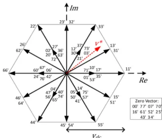
Fig. 7shows the voltage space vectors produced by the three-level OEW converter of Fig. 3. It shows also an instantaneous reference voltage vector. The switching states that produce each vector are re-presented by a two-digit number xy′, where the first digit x refer to the switching state from converter 1 and the second digit y′ refer to the state from converter 2. As an example: the state 12’ stands for Sc1, Sb1,
Sa1= 001 and Sc2, Sb2, Sa2= 010.
It is well known that in order to achieve the best modulation per-formance with respect to the output harmonic distortion, the three nearest voltage space vectors must be used to synthesize the voltage reference[26]. The vectors application times are calculated in order to achieve an average value that corresponds to the reference vector[27] and the application time of redundant vectors must be evenly dis-tributed along one switching period[28]. This modulation technique is known as space-vector modulation (SVM).
The SVM, although efficient, is a difficult technique to be im-plemented when compared to carrier-based strategies [29]. For-tunately, it has already been shown by[30](for two-level) and[23] (for multilevel converters) that the same modulation profile from SVM
Fig. 5. n-level open-end winding converter based onflying capacitor cells.
Fig. 6. Relation between the stored energy in theflying capacitors of a tradi-tional FC system compared to an OEW system.
Fig. 7. Voltage space vectors produced by an OEW three-level conversion system.
can be achieved with carrier-based PWM, if the correct common mode voltage is added to the three-phase sinusoidal references.
Fig. 8presents a block diagram of the modulation technique used in the proposed OEW configuration. It is called centered space vector pulse width modulation (CSVPWM) with state machine decoder[24].
Thefirst block inFig. 8is the calculation of a zero-sequence signal that is added to the original references in order to evenly distribute the space vectors in the switching period. This signal is calculated through ((17)-(19)), as described in[23], beingva,vbandvc the voltage
sinu-soidal references and i⊂ {a, b, c}:
′ = − + v v max( ,v v,v) min( ,v v,v) 2 i i a b c a b c (17) ″ = ⎡ ⎣ ′ + − ⎤ ⎦ v v (n 1)v v 2 mod ( ) i i dc dc (18) = ′ + − ″ ″ ″ + ″ ″ ″ v* v v v v v v v v 2 max( , , ) min( , , ) 2 i i dc a b c a b c (19)
Fig. 9presents the original voltage references, the zero sequence
signal and the resulting voltage reference (v*a) for afive-level converter.
Those resulting reference values (v *i) are then compared to
trian-gular carriers in the second block ofFig. 8. n− 1 carrier waveforms are disposed vertically between the voltage levels, with the same phase, and their frequency correspond to the switching frequency multiplied by (n− 1). The outcome of this comparison is the theoretical converter output voltage. Following the five-level converter example, the re-ference-carrier comparison and its resulting signal are presented in Fig. 10.
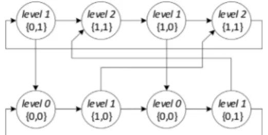
Based on the voltage levels that result from the carrier comparison, the command signals for the switching devices must be determined. This is not a simple task for multilevel converters, as different switching combinations can result in the same voltage level at the output, and this redundancy grows as the number of levels of the converter is increased. In[24]the authors proposed the use of a state machine decoder to determine the signals to command the switches in a FC structure. Fig. 11shows the example of the decoder for a three-level system: the states are the voltage levels, represented in the circles with their cor-responding switching combinations in brackets, and the arrows depict the transitions between levels.
The state machine is built in such a way that the redundant states are used to avoid uneven distribution of commutations and narrow pulses, equally distributing the losses among the switching devices and
Fig. 8. Block diagram of the CSVPWM with state machine decoder.
Fig. 9. Waveforms concerning thefirst stage of the CSVPWM with state ma-chine decoder for afive-level system: original voltage references, zero-sequence signal and resulting voltage reference.
Fig. 10. Waveforms concerning the second stage of the CSVPWM with state machine decoder for afive-level system: voltage reference-carrier comparison and theoretical converter output voltage.
F.F.V. Matos et al. Electric Power Systems Research 169 (2019) 174–183
keeping theflying capacitor voltages balanced. It grows in size as the number of levels (and redundancy) increase, as the example for a five-level system in[24], but its principle can be generalized for n-levels for a digital implementation.Fig. 12brings again the converter theoretical output voltage together with the resulting command pulses. These are the input and output, respectively, of the third andfinal block inFig. 8. As shown in the previous section, the voltage output equations of the proposed OEW structure are equivalent to those of the FC topology, which permits using the same state machine decoder. One must pay attention, however, to the fact that thefirst m1command signals are
addressed to the TOP switches of converter 1, and the other m2signals
are addressed to the BOTTOM switches of converter 2. 4. Simulation results
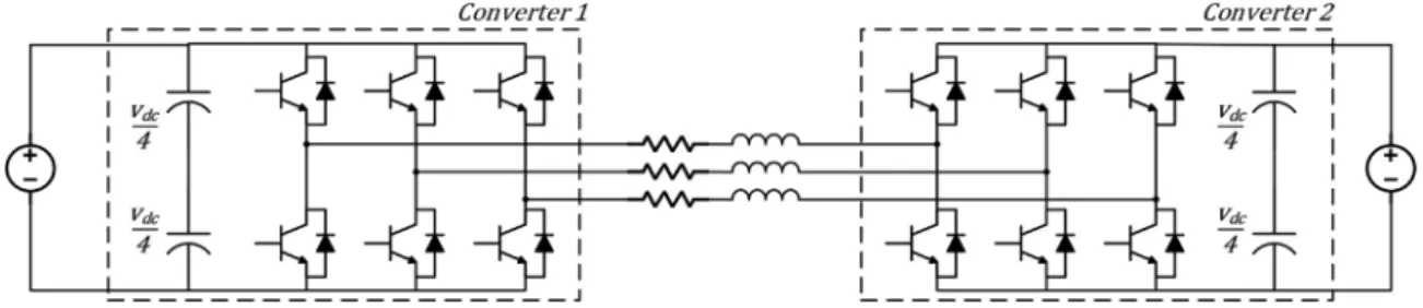
In order to exemplify the discussion presented on Section 2, two systems were simulated and compared: a five-level flying capacitor traditional drive and its equivalent OEW structure. Their circuits are illustrated in Fig. 13 and their parameters are presented inTable 1. Simulation was carried out using Plexim's PLECS®.
There are certain aspects of these systems which are important to highlight:
•
They are commanded by the same signals Sxj but, in the OEWsystem, Sx3and Sx4are directed to the bottom devices of converter
2;
•
The loads are the same (RL circuit);•
Following Eqs. (12) and (14), the traditional five-level structure demands two times the flying capacitance compared to the OEW configuration;•
Once the purpose of these simulations is to evaluate the general functioning of the systems,fixed amplitude voltage references were directly used for the modulation strategy, i.e. no control technique is employed;•
The modulation depth is determined by the relation between the peak of the reference phase voltage and the DC-link voltage:=
md vpk* /(vdc/2)
Fig. 14presents the load phase voltages produced by these systems (using the same command signals):vanfor the traditional FC andvaa′for the OEW. One can observe that the two systems produce the same load voltage, as stated in Section2by Eqs.(11)and(8).
With the same load values, and producing the same voltage, the resulting currents for both systems is also the same. For the OEW system under rated condition, the output current is presented inFig. 15and its harmonic spectrum is depicted inFig. 16. The frequency of the main current ripple is 3600 Hz. This is eight times the switching frequency, a relation that comes from the combination of two effects of the CSVPWM with state machine decoder:first, by taking advantage of the redundant switching states the resulting voltage has (n− 1) times the switching frequency; secondly, by centering the voltage space vectors in the switching period, the first commutation harmonic of the voltage is highly compensated between phases[31].
A comparison between the voltage ripple in theflying capacitors of both systems is presented inFig. 17. The shown values correspond to the capacitors connected between switches Sa1 and Sa2, which are
charged tovdc/4. Once the traditional configuration employs twice as much capacitance, it naturally presents half the voltage ripple in the capacitors.
The main concern during design, however, is the blocking voltage of the switching devices rather than the ripple of the capacitors itself. By looking at the voltage on the switch Sa2for both systems, presented in
Fig. 18, one can see how their maximum values are practically the same, even though the ripple on the capacitor voltages are different. The point here is that the switching device, in the traditional structure, stands between twoflying capacitors; therefore it can be submitted up to twice their ripple. In thefive-level OEW configuration, on the other hand, no switching device is placed between twoflying capacitors, so their blocking voltages have the same ripple as the capacitors. This example illustrate the discussion presented in Section2.3, showing that is possible to achieve the same voltage output, with the same power, but with less energy storage in the flying capacitors on the OEW structure compared to the traditional one.
The voltage balancing and stability among theflying capacitors is very important to guarantee that the switching devices are not sub-mitted to above rated voltages. For traditional FC systems, it has been already shown that the CSVPWM ensures the natural balancing of these voltages [24]. In order to show that this is also true for the OEW structure, two simulated events are presented: a start-up with un-balanced charged capacitors and a modulation depth step. The response to these events is presented inFig. 19.
At the start-up, theflying capacitors of converter 1 are charged to 90% of its nominal value, and those from converter 2 are charged to 110%. This is an abnormal condition, as the capacitors are normally precharged to their operating values, but the analysis is useful in the sense that it demonstrate how the voltages converge over time to their target values. Several precharge methods have been presented in the literature for FC converters [32–34] and could be applied to OEW systems based on FC cells. They consist in different forms of com-manding the switching devices and external contactors, in order to charge the capacitors using resistors to limit the current.
The second simulated event was a step of the modulation depth, from 1.0 to 0.5, at the instant depicted in Fig. 19. Once again, the disturbed voltages converge back to their operating values, demon-strating that the CSVPWM with state machine decoder is able to maintain the natural balance of theflying capacitors after a reference voltage transient.
Another important feature achieved by using this modulation technique in the traditional structure is the equilibrated power dis-tribution between the switching devices. In order to evaluate if this is
Fig. 11. State machine decoder for a three-level FC converter.
Fig. 12. Waveforms concerning the third stage of the CSVPWM with state machine decoder for afive-level system: converter output voltage reference and state machine resulting command signals.
also valid for the OEW system, the losses of its switching devices were calculated, according to the modeling presented by[35]. Conduction losses are determined using the transistor's collector-emitter voltage vs.
collector current curve and diode's forward voltage vs. forward current curve, supplied by the manufacturer. Instantaneous power dissipation is calculated and then averaged over one fundamental period. Switching losses are computed from the transistor's turn-on and turn-off energy curves and diode's reverse recovery energy, both functions of the con-duction current. The energy is then integrated over one fundamental
Fig. 13. Five-level simulated circuits: (a) traditionalflying capacitor and (b) its OEW equivalent structure.
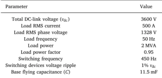
Table 1
System simulation parameters.
Parameter Value
Total DC-link voltage (vdc) 3600 V
Load RMS current 500 A Load RMS phase voltage 1328 V Load frequency 50 Hz Load power 2 MVA Load power factor 0.95 Switching frequency 450 Hz Switching devices voltage ripple 1% vdc
Baseflying capacitance (C) 11.5 mF
Fig. 14. Simulated load phase voltage for the traditional (van) and OEW systems (vaa′).
Fig. 15. Simulated load current of thefive-level OEW configuration under rated conditions.
F.F.V. Matos et al. Electric Power Systems Research 169 (2019) 174–183
period resulting in an average switching power loss.
For this study, the CM600HA-34S device, from Mitsubishi Electric, was selected. Results are presented in Fig. 20, which brings the re-sulting power dissipation per device (the sum of conduction and switching losses for transistor and diode). One can observe that the losses are equally distributed between the devices for all modulation depth range: a very interesting feature for a practical converter. It al-lows using the same modules for all the switches, which is logistically desirable and avoids overrating components.
A similar calculation was also carried out for the equivalent FC
converter, using the same device model data. It revealed that, for the entire modulation range, there is a difference under 0.002% on the total semiconductor losses between the traditional and OEW systems i.e., the losses dissipated by both structures are practically equal.
5. Experimental results
A three-level OEW converter system was tested with the purpose of verifying that the CSVPWM with state machine decoder could be suc-cessfully used in an OEW system, as discussed in the previous sections. Its power circuit is depicted inFig. 21, where it can be seen that such system does not employflying capacitors: Eq. (12) results in zero ca-pacitance. DC-links are fed by isolated DC power supplies, and the converters are connected to an RL load. The modulation strategy was programmed in PLECS® RT Box, and system parameters are presented inTable 2.
Fig. 22 shows the waveforms of the phase voltage and current, measured under rated conditions. One can observe the nine levels present in the phase voltage (vaa′) for this system:vdc[0, ± 1/6, ± 2/ 6, ± 3/6, ± 4/6]. With a commutation frequency of 450Hz, the re-sulting current presents a 1800Hz ripple, evidenced in its harmonic spectrum shown inFig. 23. This is in accordance with the previously stated effect provided by the modulation strategy: the voltage output is switched at (n− 1) times the devices commutating frequency and the first switching harmonic is highly attenuated.
A good measure of a system's performance with respect to the harmonic distortion is the current total demand distortion (TDDi), as defined by[36]. It relates the harmonic content of the current with its fundamental nominal value. Fig. 24 shows the TDDi of the output current according to the modulation depth value, with constant fun-damental frequency (50 Hz). The continuous curve was obtained from a simulation using the same parameters as the experimental setup, while the dots were obtained directly from the experimental measurements.
One can observe that the experimental results corresponded to the
Fig. 16. Harmonic spectrum of the simulated current in thefive-level OEW configuration.
Fig. 17. Flying capacitor voltage ripple comparison between the traditional and OEW systems.
Fig. 18. Sa2IGBT blocking voltage on both traditional and OEW systems.
Fig. 19. Flying capacitors voltage in thefive-level OEW system.
theoretical, and a current with TDDi under 3% is obtained even for such a small switching frequency as 450 Hz.
6. Conclusion
In this paper, a generalized OEW n-level converter using the mul-ticell flying capacitor structure was presented. A mathematical com-parison with the traditional Δ/Y structure showed that they can
produce identical voltage outputs with the same command signals. This correlation allowed the use of the CSVPWM with state machine de-coder, an optimized modulation technique originally developed for traditional FC converters, in this OEW structure.
Simulation results from afive-level structure demonstrated that the
Fig. 21. Power circuit of the dual two-level experimental setup. Table 2
Experimental setup parameters.
Parameter Value
Total DC-link voltage (vdc) 200 V
Load RMS current 10 A Load RMS phase voltage 72 V Load frequency 50 Hz
Load power 2.17 kVA Load power factor 0.95 Switching frequency 450 Hz
Fig. 22. Above: phase voltage (50 V/div). Below: load current (5A/div). Measured on the three-level system, under rated condition. Time base: 5 ms/div. Fig. 23. Harmonic spectrum of the current on the three-level system, under rated condition.
F.F.V. Matos et al. Electric Power Systems Research 169 (2019) 174–183
proposed topology provides an output with great harmonic perfor-mance, while keeping the losses evenly distributed among the switching devices. Experimental results from a three-level system showed the feasibility of a practical implementation of this system, while corro-borating the simulated results of current harmonic distortion.
Compared to a traditional FC converter with the same number of levels, the presented OEW system employs the same number of switching devices, with equal blocking voltages and dissipated losses. Its main drawback lies in the need for isolated DC-links in order to avoid the circulation of common-mode currents, thus complicating the realization of a transformerless drive. On the other hand, it has been shown that the OEW configuration demands considerably less energy storage fromflying capacitors, leading to a potential reduction in vo-lume and cost. In this context, the structure presented in this paper arises as a valuable alternative for designers of high power drive sys-tems.
Acknowledgment
The authors would like to thank the Brazilian agencies CNPq, CAPES and FAPEMIG, the French agency COFECUB and LAPLACE la-boratory, for their support to this research.
References
[1] R. Raushan, B. Mahato, K.C. Jana, Optimum structure of a generalized three-phase reduced switch multilevel inverter, Electr. Power Syst. Res. 157 (2018) 10–19. [2] J. Rodriguez, L.G. Franquelo, S. Kouro, J.I. Leon, R.C. Portillo, M.A.M. Prats,
M.A. Perez, Multilevel converters: An enabling technology for high-power appli-cations, Proceedings of the IEEE 97 (2009) 1786–1817.
[3] P. Guggenbach, H. Stemmler, Configurations of high power voltage source inverter
drives, Fifth European Conference on Power Electronics and Applications, 5 (1993) 7–14.
[4] E. Levi, M. Jones, W. Satiawan, A multiphase dual-inverter supplied drive structure for electric and hybrid electric vehicles, in: Vehicle Power and Propulsion Conference (VPPC), 2010 IEEE, IEEE, 2010, pp. 1–7.
[5] S. Mohan, J.S. TK, A. Gopinath, B. Jaya, M. Namboothiripad, Modeling and simu-lation of high power open end winding based electromechanical actuator for aerospace applications, in: Power and Advanced Control Engineering (ICPACE), 2015 International Conference on, IEEE, 2015, pp. 36–41.
[6] S. Jain, R. Karampuri, V. Somasekhar, An integrated control algorithm for a single-stage pv pumping system using an open-end winding induction motor, IEEE Trans. Ind. Electron. 63 (2) (2016) 956–965.
[7] A.S. Abdel-Khalik, A. Elserougi, A.M. Massoud, S. Ahmed, A cascaded boost in-verter-based open-end winding three-phase induction motor drive for photovoltaic-powered pumping applications, in: Electric Power and Energy Conversion Systems (EPECS), 2015 4th International Conference on, IEEE, 2015, pp. 1–6.
[8] T.A. Lipo, D. Pan, Series compensated open-winding pm generator wind generation system, 15th International Power Electronics and Motion Control Conference 7c (2012) 1–8.
[9] J. Chivite-Zabalza, I. Larrazabal, I. Zubimendi, S. Aurtenetxea, M. Zabaleta, Multi-megawatt wind turbine converter configurations suitable for off-shore applications, combining 3-l npc pebbs, IEEE Energy Conversion Congress and Exposition (2013) 2635–2640.
[10] G.A. Carlos, R.P. Sousa, C.B. Jacobina, J.P. Mello, L.M. Barros, A.C. Oliveira, Three-phase drive systems based on oew configurations with reduced controlled switch count, in: Power Electronics Conference and 1st Southern Power Electronics Conference (COBEP/SPEC), 2015 IEEE 13th Brazilian, IEEE, 2015, pp. 1–6. [11] M. Darijevic, M. Jones, E. Levi, An open-end winding four-levelfive-phase drive,
IEEE Trans. Ind. Electr. 63 (1) (2016) 538–549.
[12] T.A. Lipo, Y. Wang, D. Panda, D. Pan, Open-winding power conversion systems fed by half-controlled converters, IEEE Trans. Power Electr. 28 (2013) 2427–2436. [13] C.B. Jacobina, N. Rocha, N.S.M.L. Marinus, Open-end winding permanent magnet
synchronous generator system with reduced controlled switch count, Brazilian Power Electronics Conference (2013) 692–698.
[14] A.K. Yadav, K. Gopakumar, Krishna raj. R, Loganathan Umanand, Kouki Matsuse GAE, Hisao Kubota, Instantaneous balancing of neutral point voltages for stacked DC-link capacitors of multilevel inverter for dual inverter fed induction motor drives, IEEE Transactions on Power Electronics (2018) 1,https://doi.org/10. 1109/TPEL.2018.2837680.
[15] K. Gopakumar, E. Shivakumar, S.K. Sinha, A. Pittet, V.T. Ranganathan, Space vector pwm control of dual inverter fed open-end winding induction motor drive, Sixteenth Annual IEEE Applied Power Electronics Conference and Exposition 1 (2001) 399–405.
[16] V. Somasekhar, S. Srinivas, K. Gopakkumar, A space vector based pwm switching scheme for the reduction of common-mode voltages for a dual inverter fed open-end winding induction motor drive, in: Power Electronics Specialists Conference, 2005. PESC’05. IEEE 36th, IEEE, 2005, pp. 816–821.
[17] S. Srinivas, V. Somasekhar, Space-vector-based PWM switching strategies for a three-level dual-inverter-fed open-end winding induction motor drive and their comparative evaluation, IET Electric Power Applications 2 (1) (2008) 19–31. [18] M. Baiju, K. Mohapatra, K. Gopakumar, Pwm signal generation for dual inverter fed
open-end winding induction motor drive using only the instantaneous reference phase amplitudes, in: Power Electronics and Drive Systems, 2003. PEDS 2003. The Fifth International Conference on, Vol. 1, IEEE, 2003, pp. 450–455.
[19] D.S. George, M. Baiju, Decoupled random modulation technique for an open-end winding induction motor based 3-level inverter, in: Industrial Electronics & Applications, 2009. ISIEA 2009. IEEE Symposium on, Vol. 2, IEEE, 2009, pp. 1022–1027.
[20] G.d.A. Carlos, E. dos Santos, C. Jacobina, Hybrid pwm strategy for voltage source inverters feeding three-phase open-end-winding equipment, in: IECon 2012-38th Annual Conference on IEEE Industrial Electronics Society, IEEE (2012) 459–464. [21] F.F.V. Matos, H.d.O. Ramos, D.C.G. Rocha, R.M. da Silva, M.A.S. Mendes,
V.F. Mendes, A multilevel wind power conversion system with an open winding squirrel cage induction generator, in: Proc. IEEE 13th Brazilian Power Electronics Conf. and 1st Southern Power Electronics Conf. (COBEP/SPEC), doi:10.1109/ COBEP.2015.7420248, 2015, pp. 1–6.
[22] F.F.V. Matos, H.O. Ramos, C.E. Oliveira, V.F. Mendes, M.A.S. Mendes, T. Meynard, A vector modulation strategy for open-end winding conversion systems, in: Proc. IEEE Int. Conf. Industrial Technology (ICIT), doi:10.1109/ICIT.2018.8352249, 2018, pp. 617–622.
[23] B.P. McGrath, D.G. Holmes, T. Lipo, Optimized space vector switching sequences for multilevel inverters, IEEE Trans. Power Electron. 18 (6) (2003) 1293–1301,
https://doi.org/10.1109/TPEL.2003.818827.
[24] B.P. McGrath, T. Meynard, G. Gateau, D.G. Holmes, Optimal modulation offlying capacitor and stacked multicell converters using a state machine decoder, IEEE Trans. Power Electron. 22 (2) (2007) 508–516,https://doi.org/10.1109/TPEL. 2006.889932.
[25] T. Meynard, H. Foch, Multi-level choppers for high voltage applications, EPE journal 2 (1) (1992) 45–50.
[26] N. Celanovic, D. Boroyevich, A fast space-vector modulation algorithm for multi-level three-phase converters, IEEE Transactions on Industry Applications 37 (2) (2001) 637–641,https://doi.org/10.1109/28.913731.
[27] Y.-H. Lee, B.-S. Suh, D.-S. Hyun, A novel PWM scheme for a three-level voltage source inverter with gto thyristors, IEEE Trans. Ind. Appl. 32 (2) (1996) 260–268,
https://doi.org/10.1109/28.491473.
[28] S. Fukuda, Y. Iwaji, A single-chip microprocessor-based PWM technique for sinu-soidal inverters, in: Proc. Conf. Record of the 1988 IEEE Industry Applications Society Annual Meeting, vol.1. doi:10.1109/IAS.1988.25170, 1988, pp. 921–926. [29] G. Carrara, S. Gardella, M. Marchesoni, R. Salutari, G. Sciutto, A new multilevel
pwm method: A theoretical analysis, IEEE Trans. Power Electron. 7 (3) (1992) 497–505.
[30] D.G. Holmes, The general relationship between regular-sampled pulse-width-mod-ulation and space vector modpulse-width-mod-ulation for hard switched converters, in: Proc. Conf. Record of the 1992 IEEE Industry Applications Society Annual Meeting, vol.1. doi:10.1109/IAS.1992.244437, 1992, pp. 1002–1009.
[31] E. Monmasson, Commande rapprochée de convertisseur statique, Vol. 1, Hermes Science Publications, 2009.
[32] S. Pirog, M. Baszynski, J. Czekonski, S. Gasiorek, A. Mondzik, A. Penczek, R. Stala, Multicell DC/dc converter with DSP/CPLD control. practical results, in: Proc. 12th Int. Power Electronics and Motion Control Conf, doi:10.1109/
EPEPEMC.2006.4778479, 2006, pp. 677–682.
[33] H. Sepahvand, M. Khazraei, M. Ferdowsi, K.A. Corzine, Capacitor voltage regulation and pre-charge routine for aflying capacitor active rectifier, in: Proc. IEEE Energy Conversion Congress and Exposition (ECCE), doi:10.1109/ECCE.2012.6342265, 2012, pp. 4107–4112.
[34] D. Janik, T. Kosan, P. Kamenicky, Z. Peroutka, Universal precharging method for dc-link andflying capacitors of four-level flying capacitor converter, in: Proc. IECON 2013-39th Annual Conf. of the IEEE Industrial Electronics Society, doi:10.1109/IECON.2013.6700175, 2013, pp. 6322–6327.
[35] K. Ma, A.S. Bahman, S. Beczkowski, F. Blaabjerg, Complete loss and thermal model of power semiconductors including device rating information, IEEE Trans. Power Electron. 30 (5) (2015) 2556–2569,https://doi.org/10.1109/TPEL.2014.2352341. [36] IEEE recommended practice and requirements for harmonic control in electric
power systems, IEEE Std 519-2014 (Revision of IEEE Std 519-1992) (2014) 1-29. doi:10.1109/IEEESTD.2014.6826459.
Fig. 24. Total demand distortion of the current on the three-level system: si-mulated and experimental data.