Contact Thermal Lithography
by
Aaron Jerome Schmidt
Submitted to the Department of Mechanical Engineering
in partial fulfillment of the requirements for the degree of
Master of Science in Mechanical Engineering
at the
MASSACHUSETTS INSTITUTE OF TECHNOLOGY
May 2004
@
Massachusetts Institute of Technology 2004. All rights reserved.
Author
Department of Mechanical Engineering
May 18, 2004
C ertified by ...
...
Gang Chen
Professor
Thesis Supervisor
A ccepted by ...
...
Ain Sonin
Chairman, Department Committee on Graduate Students
MASSACHUSETTS INS1TJJTE OF TECHNOLOGY
Contact Thermal Lithography
by
Aaron Jerome Schmidt
Submitted to the Department of Mechanical Engineering on May 18, 2004, in partial fulfillment of the
requirements for the degree of
Master of Science in Mechanical Engineering
Abstract
Contact thermal lithography is a method for fabricating microscale patterns using heat transfer. In contrast to photolithography, where the minimum achievable feature size is proportional to the wavelength of light used in the exposure process, thermal lithography is limited by a thermal diffusion length scale and the geometry of the situation. In this thesis the basic principles of thermal lithography are presented. A traditional chrome-glass photomask is brought into contact with a wafer coated with a thermally sensitive polymer. The mask-wafer combination is flashed briefly with high intensity light, causing the chrome features heat up and conduct heat locally to the polymer, transferring a pattern. Analytic and finite element models are presented to analyze the heating process and select appropriate geometries and heating times. In addition, an experimental version of a contact thermal lithography system has been constructed and tested. Early results from this system are presented, along with plans for future development.
Thesis Supervisor: Gang Chen Title: Professor
Acknowledgments
This work could not have been completed without the support of many people. First among these is my advisor, Professor Gang Chen. His guidance, wisdom and good humor made the entire process enjoyable. Kurt Broderick in EML was instrumental in the fabrication and testing of samples. He always took time to share his expertise and offer advice. Dr. James Goodberlet provided plans for the vacuum sample holder and shared his knowledge on contact lithography, and Dr. Xiaoyuan Chen taught me some basic optics and kept our laser running smoothly. I would also like to thank all the members of the Nanoengineering Group, who were always willing to listen to ideas and give back new ones.
I am indebted to my family for their unconditional support in all my endeavors,
and to Jennifer Yu for keeping me well rounded. Finally, thanks to the Department of Defense for their generous financial support.
Contents
1 Introduction 11
1.1 Background . . . . 11
1.2 Contact Thermal Lithography . . . . 15
2 Modeling 17 2.1 Basic Approach . . . . 17
2.2 Optical Modeling . . . . 18
2.3 Thermal Modeling . . . . 24
2.3.1 Limitations and Assumptions . . . . 24
2.3.2 Analytic Solutions . . . . 26 2.3.3 Numerical Solutions . . . . 29 3 Experimental Setup 39 3.1 O ptics . . . . 40 3.2 Wafer Stage . . . . 44 3.3 Materials Selection . . . . 47
4 Method and Results 49 4.1 The CTL Process Flow . . . . 49
4.2 R esults . . . . 51
5 Discussion and Conclusion 55 5.1 Short Term Goals . . . . 55
5.2 Long Term Goals and Commercial Potential . . . . 57 7
5.3 Conclusion . . . . 58
A Material Properties 59
A.1 Optical Properties . . . . 59 A.2 Thermal Properties . . . . 62
List of Figures
1-1 Projection photolithography
Nano Imprint Lithography . . . . Contact Thermal Lithography geometry . . . . The CTL process flow . . . .
Reflection and absorption by a photomask . . . . Reflectivity of the mask structure for three metals . . .
The 95% absorption length of 3 metals . . . . Mask with a thin metal layer . . . . Optical properties for a thin metal layer . . . . Simple 1D representation of the conduction problem . . Thermal capacity of the metal layer . . . . Temperature in the polymer layer . . . .
2D model used in ADINA finite element analysis . . . . A typical ADINA mesh . . . . A temperature contour plot . . . .
Time evolution of the lateral temperature profile . . . .
Lateral temperature profile along the resist top surface
2D model with reduced dimensions . . . .
Lateral temperature profile for the reduced model . . .
Schematic of the basic CTL system . . . . Optical pulse generation system . . . . Pulse length as a function of angular step size . . . . .
9 . . . . 12 1-2 1-3 1-4 2-1 2-2 2-3 2-4 2-5 2-6 2-7 2-8 2-9 2-10 2-11 2-12 2-13 2-14 2-15 3-1 3-2 3-3 . . . . . 13 . . . . . 15 . . . . . 16 . . . . . 19 . . . . . 21 . . . . . 22 . . . . . 23 . . . . . 23 . . . . . 26 . . . . . 28 . . . . . 29 . . . . . 31 . . . . . 32 . . . . . 33 . . . . . 34 . . . . . 35 . . . . . 36 . . . . . 36 40 41 42
3-4 3-5 3-6 3-7 3-8 3-9 3-10 4-1 4-2 4-3 4-4
4-5 The boundary between a region of solid Cr and clear glass
B-1 LabVIEW interface for the CTL system. . . . . Beam profiling apparatus . . . .
A typical beam profile . . . .
Vacuum wafer fixture . . . . Groove cut on the bottom plate . . . . Vacuum wafer with top seal in place. . . . .
Newton's rings between the mask and wafer . . . .
Vacuum wafer assembly mounted on a motion stage
The exposure procedure . . . . Early test results . . . . Resist regions torn by adhesion . . . . Images of the photomasks following laser exposure .
. . . . 43 . . . . 43 . . . . 45 . . . . 45 . . . . 46 . . . . 46 . . . . 47 . . . . 51 . . . . 52 . . . . 53 . . . . 53 . . . . 54 64
Chapter 1
Introduction
1.1
Background
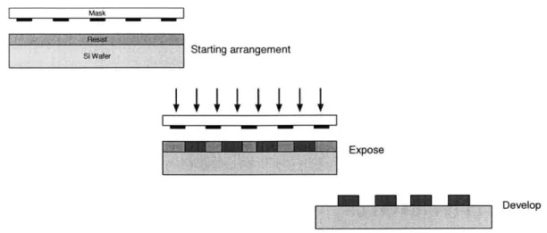
Photolithography is the industry-standard method by which microelectronic circuits and other small-scale devices are produced. The basic procedure, depicted in Figure
1-1, is simple: light is projected through a mask onto a wafer coated with a polymer film
known as photoresist. The light causes a chemical change in the exposed regions of the resist, and subsequent development with an appropriate solvent washes away either the exposed or unexposed regions, depending on the resist chemistry. The remaining pattern is then used as a mask to protect the underlying area. The minimum feature size this method can achieve is proportional to the wavelength of light employed in the exposure process:
Wmin = -- (A1
NA
Here A is the wavelength, NA is the numerical aperture of the exposure system, and
k is a parameter of the system.
Photolithography can be done in contact mode or projection mode. In contact mode, the mask is placed directly on the wafer, while in projection mode there is a gap between the two. Projection photolithography is the current industry standard. It allows for greater throughput, simpler mask alignment and optical reduction of the mask features on the wafer. However, contact lithography has potential advantages
Mask
Starting arrangement
Expose
Develop
Figure 1-1: Projection photolithography. Light shines through a mask and exposes photoresist. Development transfers the mask pattern.
resulting from near-field optical effects and is also being actively developed.[1] In an ongoing effort to fit more features into smaller spaces, engineers have been improving each term of equation 1.1. The parameter k depends on the exposure tool, the mask, and properties of the photoresist. Through advances in exposure optics, phase-shifting mask features and resist chemistries, k has been reduced to around 0.4 in the best cases. There is little room left for improvement, however, because for spatially incoherent illumination k has a theoretical minimum of 0.25. The numerical aperture of high-performance lithography systems is in the neighborhood of 0.6, and techniques such as liquid immersion may boost this number closer to one. Such techniques will also increase the cost and complexity of exposure systems. Finally, the semiconductor industry has been steadily decreasing exposure wavelength. The most current technology uses 193 nm light, and a future shift to 157 nm is expected. Unfortunately, each advance requires new and expensive lens technology utilizing exotic materials such as CaF2.
The cumulative effect of all these efforts has been that the number of features on a semiconductor chip has roughly doubled every 18 months for the past three decades. Unfortunately, this progress has been accompanied by exponentially increasing capital costs.[2] Individual fabrication tools, such as lithography steppers, have reached tens of millions of dollars, and complete modern fabrication facilities require investments
of several billion dollars. If this trend continues, economic constraints will seriously limit lithographic progress.
Fortunately, there are a number of alternative lithographic techniques that have emerged in recent years. Common to many of these techniques is that the resolu-tion has been uncoupled from an exposure wavelength. This frees them from many challenges facing traditional lithography and provides hope for avoiding escalating capital costs. One of the best known alternative lithographies is known as Nano Imprint Lithography (NIL).[3] NIL has produced features as fine as 10 nm and has spawned a number of similar techniques for pattern transfer.[4]
Conceptually, NIL is simple. A rigid template consisting of raised features is pressed into a polymer resist, creating an imprint. Subsequent etching transfers this imprint to the substrate below. The basic process is depicted in Figure 1-2. The templates are typically fabricated on quartz substrates using conventional electron beam lithography, which has excellent resolution but poor throughput. The imprint-ing layer is normally polymethylmethacrylate (PMMA) which has been heated above its glass transition temperature of roughly 105 'C, and the required imprint pressure is between 10 and 100 MPa.
Quartz Template
Sub~stratia
Imprint
Release
Etch
Figure 1-2: Nano Imprint Lithography (NIL). A rigid template is pressed into a maleable polymer layer, creating an imprint. Etching removes the depressed regions, leaving behind a pattern that serves as a mask for future processes.
NIL has had success reproducing a wide variety of patterns and even some
func-tional devices.[5] However, it has important limitations. Certain types of patterns are difficult to imprint, particularly isolated recessed features. The high pressures in-volved require large forces for even moderately sized templates, and the pressures can deform the underlying substrate, posing a challenge for the fabrication of multi-layer structures. In addition, a planarization step is required between layers in multilevel structures. Finally, issues such as thermal expansion and layer-to-layer alignment limit the ability to produce complex multi-template devices.[6]
Variants on the NIL process have attempted to address some of these limitations. One such variant is Step and Flash Imprint Lithography (SFIL).[7] In SFIL, a low viscosity, photopolymerizable polymer is dispensed onto a wafer. A template is then pressed onto the wafer, displacing the polymer and causing it to fill the template relief patterns. With the template still in contact, the polymer is cured with UV light. The template is then removed, leaving behind the patterned and cured polymer.
Like NIL, SFIL appears only to be limited by the template resolution, and features down to 20 nm have been reproduced.[8] However, pressures less than 5 MPa are needed to fill typical patterns.[9] This greatly reduces the required imprinting force and the risk of deformation. SFIL also does not require high temperatures, minimizing thermal expansion. A key challenge for SFIL is imprint thickness and uniformity over large substrate areas. This requires great control in the way droplets of liquid photopolymer are dispensed over the surface. SFIL also must contend with some of the same issues as NIL, including multilayer alignment and planarization.
There are numerous other alternative lithographies being developed. These in-clude laser-assisted NIL, micro-contact printing and various scanning probe direct write techniques.[6] Each has its own strengths and weaknesses, and most are contin-ually being improved. It is hoped that one or a combination of such new techniques will be able to meet future micro- and nano-fabrication requirements.
1.2
Contact Thermal Lithography
Contact Thermal Lithography (CTL) is a new approach to fabrication. It incorporates aspects of contact photolithography and NIL but is distinct from both. The concept is straightforward: a mask consisting of metal patterned on glass is brought into contact with a wafer that has been coated with a thermally sensitive polymer referred to as thermoresist. The combination is flashed briefly with a high intensity laser of visible wavelength. The patterned metal features are strongly absorbing and rapidly heat up, while the optically transparent glass and polymer do not. Due to the short flash duration, the metal conducts heats only to the directly contacted polymer, causing local crosslinking. After the mask is removed the wafer is developed in an appropriate solution, leaving behind only the crosslinked regions. Because the underlying wafer may be optically absorbing, a thermal buffer layer such as SiO2 is required between the wafer and the thermoresist. The mask-wafer arrangement is depicted in Figure
1-3 and a representation of the process flow is shown in Figure 1-4.
111 1 1 11 1Visible Radiation
Glass Mask Substrate
Metal Feature
Crosslinked _ Region
Oxide Buffer Layer
Figure 1-3: Basic Contact Thermal Lithography (CTL) geometry. Radiation incident on the mask heats up the metal feature. The heat is conducted to the underlying polymer, causing crosslinking.
Unlike NIL and SFIL, contact thermal lithography requires only enough pressure to ensure intimate contact between the mask and wafer. In addition, it can reproduce truly arbitrary features without concern for the flowing and redistribution of an
=
ReleaseEtch
Figure 1-4: The CTL process flow. The SiO2 buffer layer has been omitted for clarity.
printing layer. It also promises high throughput due to the extremely short heat-cool cycle. Like all contact lithography techniques CTL faces challenges with regard to surface planarization and multi-layer alignment, but these issues are being dealt with
by numerous research and commercial groups.[6]
The goal of this thesis is to demonstrate the feasibility of contact thermal lithog-raphy. Criteria for the selection of mask and resist materials are discussed, along with the fundamental limits imposed by the optical and thermal characteristics of the situation. These details are covered in the next chapter. Chapter 3 describes in detail a simple, proof-of-concept implementation of a CTL system that has been constructed. This system is built around easily obtainable materials and photomasks. As a result, the target resolution is on the order of microns instead of nanometers. However, the early implementation highlights several potential issues with a CTL system and has the potential to be extended to smaller feature reproduction. The experimental procedure and some results produced by this system are presented in
Chapter 4, including a discussion of a number of difficulties that were encountered. Chapter 5 summarizes the research and examines future challenges and opportunities for this new technology.
Contact
Chapter 2
Modeling
2.1
Basic Approach
Modeling CTL involves optical, thermal and materials problems. Here the focus is primarily on the optical and thermal problems; a theoretical treatment of the materials issues is left for future work.
The optical problem is fairly simple. High intensity, monochromatic light impinges on a stack of materials at normal incidence. The stack consists of some type of glass, a thin metallic layer, and a thermally sensitive polymer. Given the intensity and wavelength of the source, the goal is to predict the rate at which energy is absorbed
by the metallic layer. Using electromagnetic theory, the portions of energy that are
reflected, absorbed and transmitted are calculated.
Once the conversion rate between optical and thermal energy is known, the ther-mal behavior of the system can be modeled. The dominant mode of heat transfer from the metal to the polymer is conduction. The transient heat transfer character-istics are estimated with a simple 1-D model. A finite element model is used to make a more precise 2-D estimate of the temperature evolution in the polymer resist layer. For a given resist material, there will be a threshold temperature above which polymer crosslinking occurs. The transient heating characteristics of the polymer are used to deduce the appropriate optical intensity and exposure time necessary to cure the resist through its thickness. These parameters will depend on the specific material
properties of the mask and the resist, as well as the thickness of the resist layer.
2.2
Optical Modeling
The purpose of the photomask in normal photolithography is to reduce optical in-tensity to zero in the masked areas. In thermal lithography, however, the ideal mask absorbs the maximum optical energy, regardless of the amount of transmitted light. This distinction is explored in this section. The simplest case, in which the metal layer is sufficiently thick to absorb all incoming light, is examined first. It is the case that most closely matches the experimental setup, and the analysis used is general enough to then be easily extended to the thin-layer case.
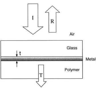
Figure 2-1 shows a model of the mask in cross section. Monochromatic light at normal incidence strikes the glass surface with intensity I. Some portion R is reflected back toward the source, and the remainder T is ultimately absorbed by the metallic layer. It is necessary to calculate the fraction of absorbed energy in order to determine the heating rate in the metal. It is assumed that the metal layer is sufficiently thick to absorb the transmitted radiation. This assumption will be justified later.
The optical properties of layered structures have been studied extensively. If the optical properties of the constituent materials are known, it is a simple matter to calculate the overall properties of the layered structure. In many situations, it is difficult to calculate the reflectivity and transmissivity of materials due to the scattering of light by microscopic peaks and valleys on the surface. However, in the case when the surface is optically smooth (when surface variations are smaller than the optical wavelength), the reflectivity and transmissivity can be found using the standard Fresnel coefficients. Under the condition of normal incidence, the reflectivity is given by
R = (2.1)
R N2 + N1
where N1 and N2 are the indices of refraction of materials 1 and 2, respectively. The
result holds for absorbing materials, in which case N will be have an imaginary part. This result, valid for a single interface, can be extended to a series of interfaces.
R
Air
Glass
T
Figure 2-1: Reflection and absorption by a photomask. A fraction of the incoming intensity is reflected by the Air-Glass and Glass-Metal interfaces, and the rest is transmitted into and absorbed by the metal layer.
There are two approaches to this problem, ray tracing and wave optics. The ray tracing approach is simpler. At each interface the reflected and transmitted inten-sities are tabulated, and the endless internal reflections are summed up simply in a geometric series, giving the net properties for the stack. This approach neglects any phase information carried by the electromagnetic waves. If the individual layers are thick compared to the wavelength and the coherence length of the source, then the approximation is good. As the layer size shrinks, however, interference effects will alter the results.
The alternative approach is to solve the full set of electromagnetic equations in-side each layer under the constraint that the fields match correctly at the interfaces. This can be done in matrix format, in an approach known as the transfer matrix method. [10] Equation (2.2) gives the reflectivity for a layered structure containing m layers:
l (i 1 1 + m12Pm+l)PO - (M 2 1 + M22Pm+1) 2
R (m11 + m12Pm+1)Po + (M2 1 + M2 2Pm+i) (2.2)
The subscripts 0 and m + 1 indicate the media on either side of the layered structure
and the elements mij are taken from the overall transfer matrix M given by
M - ]~J in1 1 M1 2
j=1 M2 1 M2 2
The individual transfer matrices Mi are given by
cos j - Lsin 4#
-ipj sin Oj cos
#
jwhere
wNjdj cos Oj
Co
Pj,TM = 0 s Oj
Pj,TE = Cos Oj
Here w is the radiation frequency, Nj and dj are the index of refraction and thickness of the Jth layer, 0, is the propagation direction and cj and pj are the electric permit-tivity and magnetic permeability of the Jth layer. c0 is the speed of light in vacuum and the subscripts TM and TE denote transverse magnetic and transverse electric polarizations. For normal incidence, all Oj = 0 and the TM and TE cases reduce to the same result.
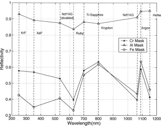
Equation (2.2) was used to calculate the reflectivity of the structure shown in Fig-ure 2-1. Although the photomask structFig-ure is much thicker than optical wavelengths, the coherence length of a laser can be meters or kilometers long and equation (2.2) will capture the resulting interference effects. Of course, the surfaces still must be parallel and optically smooth or the results will not be accurate. The mask substrate is assumed to be fused silica, with a thickness of 500 pm. The results are shown in Figure 2-2 as a function of wavelength for three common metals, Cr, Al and Fe. The reflectivity is shown only at some common laser wavelengths. The optical properties of the various materials used in calculation are given in Appendix A.
NdYAG iTi-Sapphire NdAG HeNe 0.9 - -.. . . (doubled Krypton: Argori 0.8 KrF XeF -+--Cr Mask -Al Mask .. 7 -.-.-.-.- . e Fe Mask > 14-1 0 .5 - - - -.-0 .4 - - . -. -.-- - .-.- - .-.-.-.-0.3 200 300 400 500 600 700 800 900 1000 1100 1200 Wavelength(nm)
Figure 2-2: Reflectivity of the mask structure for three types of metal layer. The results are calculated at some common laser wavelengths.
In the thick-film case, the majority of the light transmitted into the metallic layer should be absorbed and converted to heat, so that the volumetric heating rate
Q
= 1(1 - R)/t where t is the thickness of the metal. This is ensured by giving the layer adequate thickness. The rate at which intensity decays inside an absorbing material is given by-47rr((A)z
I, = Ix(0) exp A(23)
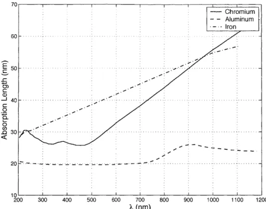
Here, I\(O) is the initial intensity, z is the distance into the material, and r. is the imaginary portion of the complex index of refraction N = N - in. Using the known optical properties listed in Appendix A, the thickness required to reduce a propagating wave to 5% of its original intensity is plotted for three metals in Figure 2-3. This result serves as a guide for the necessary metal thickness depending on the exposure wavelength.
It is possible to achieve significantly higher absorption than the case of a very
70
60-0
200 300 400 500 600 700 800 900 1000 1100 1200
X(nm)
Figure 2-3: The 95% absorption length plotted as a function of wavelength for 3 metals.
thick metal layer. If the mask is not required to reduce optical transmittance to zero, wave interference effects may enhance the absorbed optical energy. Consider for example the situation depicted in Figure 2-4, where the transmitted energy may be significant. For a given wavelength A, the reflectivity, transmissivity and absorptivity will all be functions of the metal layer thickness.
To illustrate this, the absorptivity of a thin film of Cr was calculated using equation (2.2). The results are plotted in Figure 2-5. The particular wavelength chosen was
532 nm and the thickness t was varied between zero and 70 nm. At a metal thickness
of 8.5 nm, the absorptivity of the layer has a value 25% higher than that predicted for an infinitely thick metal layer. As the thickness t increases, the optical properties approach those of the thick-layer case and the reflectivity is equal to that shown in Figure 2-2 for a Cr film at 532 nm.
Although optimizing the film thickness for maximum absorptivity is desirable,
- Chromium
- Aluminum -- Iron
R
Air
Metal
Figure 2-4: A mask with a thin metal layer in contact with a polymer resist. Although the transmitted intensity is not reduced to zero, absorption may be higher than the case shown in Figure 2-1
CD) (D 0. a. 0 0 0.9 0.8 0.7 0.6 0.5 0.4 0.3 0.2 0.1 01 C 10 20 30 40 50 60 70 Metal Thickness (nm)
Figure 2-5: Optical properties for the structure shown in Figure 2-4. At a metal thickness of 8.5 nm, the absorptivity of the film reaches its maximum value.
23 Glass t t-Polymer T Asrptivityvt -.- .... -...-.. - ... ... ... ... -. -. ...-. -. -. ... -......- ...-. ...
practical concerns may impose additional constraints. The durability of the metal features may be compromised as the layer thickness shrinks. In addition, many coat-ing processes require a minimum thickness to ensure even coverage. Dependcoat-ing on the metal and coating process being used, these effects must also be considered.
2.3
Thermal Modeling
2.3.1
Limitations and Assumptions
Transient heat conduction in isotropic bulk solids is governed by the diffusion equation
pc T =
+
kV2 T (2.4)at
where T is temperature, p the density, c the specific heat capacity, 4 the volumetric heat generation term, and k the thermal conductivity. Solutions to this equation will comprise the majority of the analysis presented here. There are, however, limits to equation (2.4)'s applicability, particularly when the characteristic dimensions of the problem are very small or when molecular orientation results in anisotropies. It is necessary to explore these limits before proceeding.
In dielectric (non-conducting) solids, energy is primarily carried by quantized lattice vibrations known as phonons. Energy transport can accurately be modeled as a diffusion process when the distance a phonon travels between collisions with other phonons is small compared to the dimensions of the structure. This inter-collision distance is referred to as the mean free path. In addition, the intrinsic quantum wavelength of the carrier itself should be smaller than the dimensions of the structure. If either of these conditions is not satisfied, energy transport can be modeled using ballistic transport theory or, if necessary, quantum mechanics.[11]
The mean free path 1(T) for amorphous dielectrics can be approximated as
3K(T)
where K is the thermal conductivity, v is the average phonon velocity and C is the volumetric heat capacity.[12] Using this method, the mean free path has been calculated for a number amorphous solids. For typical materials such as PMMA or amorphous SiO2, 1 < 10
A
for T > 100 K.[12] At 300 K, a typical phonon wavelengthis also on the order of 10
A.[11]
Thus, for amorphous structures with dimensions of10 nm or more the diffusion model is adequate and equation (2.4) applies.
Isotropy is more difficult to justify. Polymers are often composed of very long and complex molecules, and when the polymer is applied in a thin film the molecules tend to align themselves in a preferred orientation. This can potentially impact both thermal and mechanical properties. Unfortunately, there is no simple way to predict whether or not anisotropy will occur. When a polymer is drawn in a given direction, thermal conductivity tends to increase in the drawn direction and decrease in the perpendicular direction. Depending on the polymer and the degree of drawing, departure from the bulk isotropic conductivity may be anywhere from 1% to 50%.[12] The thermal properties of very few polymers have been studied in a thin film configuration. Those studies that have been done do not indicate a simple pattern. For example, the ratio of in-plane to out-of-plane thermal conductivity for
PMDA-ODA polyimide films is expected to asymptotically approach a value of 10 as film
thickness decreases below 1 pm. [13] On the other hand, similar work with PMMA has shown no appreciable anisotropy. [14] In the latter case, however, thermal conductivity was shown to be roughly 2/3 the bulk value. To complicate matters further, thermal conductivity is a function of both temperature and the degree of crosslinking in the polymer.
Therefore, to accurately asses the thermal characteristics of a given polymer in a thin film configuration, it is necessary to perform a detailed study of that particular polymer under conditions similar to those of the actual exposure process. For the sake of simplicity, it is assumed here that the thermoresist film has isotropic material properties similar to those of PMMA. The following analysis should be modified to account for more complex material behavior if data is available.
2.3.2
Analytic Solutions
Keeping the above limitations in mind, equation (2.4) is used to model the thermal behavior of a CTL system. In most cases it is not possible to obtain analytic solutions to this equation. However, exact solutions for simple 1D situations are available, and these can give insight into more complex problems.
Figure 2-6 depicts a simplified 1D model of the mask-wafer arrangement. It con-sists of a heat-generating layer sandwiched between two different materials, repre-senting the glass-metal-polymer arrangement of CTL. This model will not yield any insight into lateral heat conduction and edge effects, but will give an indication of the time and temperature scales involved in the problem.
k2
,
pc2
ki, pci2 q1
Figure 2-6: Simple 1D representation of the conduction problem
A solution for this case can be built on the solution to an even simpler problem
- a semi-infinite surface subjected to constant heat flux. For such a situation, the solution is given by [15]
TX'(t) = T +
j
ercf(x/2vfH)dx (2.6)Here Tx,(t) is the temperature at distance x' from the surface of the body at time t,
Ti is the initial temperature of the body, q, is the heat flux at the surface, a is the
the surface where x' = 0, this reduces to
T,(t) = T + 2 (2.7)
k i2 rl
In order to apply equation (2.6) to the model shown in Figure 2-6, two conditions must be satisfied: the energy that goes into heating the metal absorber must be negligible compared to the flux into the two semi-infinite bodies, and the ratio of the heat fluxes into the two semi-infinite bodies must be constant. It is simplest to assume the former condition holds and prove the latter, and then verify that the assumption was valid.
Assuming both surfaces have the same initial temperature and that there is no temperature gradient across the thin metal layer, both bodies must have the same surface temperature. Then,
k1 a1t _t k2 Fx~t
The ratio q1
/q
2 is indeed constant and is given by_ qi _ ki a2 (28)
q2 k2 a1
Thus each side of the model can be treated as an isolated case that can be solved with equation (2.6) using a value of q, that has been reduced by the appropriate fraction. It is now straightforward to verify that the metal layer absorbs a negligible amount of energy. This condition is expressed as
dT
C--
<
q1 + q2dt
where C is the heat capacity of the metal layer. Using equations (2.7) and (2.8), this becomes
Ca, = (2.9)
k +^1 ) a7rt
Figure 2-7 plots the quantity
#
as a function of time using representative proper-ties. The metal layer is Cr and is 50 nm thick. Material 1 is a typical polymer andmaterial 2 is glass. Depending on the material properties, 7-1 ranges between 3 and
15; the value used here was 5. As the figure shows, the thermal capacity of the metal
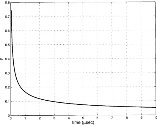
layer will have an impact only for the very early stage of heating. Thus solutions ignoring this thermal capacity will overestimate the flux into the semi-infinite bodies for the first microsecond of heating but will become increasingly accurate as time progresses. 0.8 0.7 0.6 0.5 re 0.4 0.3 0.2 0.1 0 0 I I I I I I I I I I I I I I I 2 3 4 5 6 7 8 9 10 time ( sec)
Figure 2-7: The quantity 13 plotted against time. The thermal capacity of the metal layer has negligible importance for
#
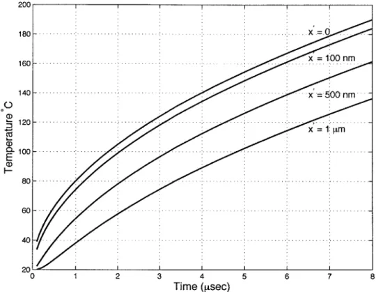
<K 1Neglecting the heat capacity of the metal layer, equation (2.6) can now be used to predict the temperature propagation through semi-infinite bodies 1 and 2. In this particular problem, only the temperature distribution in the polymer layer is of interest; this information reveals when and where crosslinking will occur. Figure 2-8 plots the temperature in the polymer layer as a function of time for various positions inside the layer. As in Figure 2-7, representative values for the material properties
with the typical heat fluxes used in the actual experiments. The initial temperature was taken as 20 'C. The thermally sensitive polymers considered in this experiment have crosslinking temperatures between 100 and 200 'C. Figure 2-8 indicates that it should take less than 10 psec to cure a 500 nm resist layer.
20 18 16 14 "12 CL10 E 8 6 4 0 ... -.. -. .. x..= 1.00. nm -0 - - - ---.- -0x=1.m 0 - - - - --. -. -.-. ---.- -. -. -0 -~~~~ -- - - - -L-M- - ~~ ..-.. - . -... -... -.-.-.-.. ---.-. 0 - - - .- --.-- . -.-.-1 2 3 4 Time ([tsec) 5 6 7 8
Figure 2-8: Temperature in the polymer layer as a function of time for various posi-tions inside the layer. Typical material properties and a heat flux of 4.25 x 10⁷ W/m 2
were used
2.3.3
Numerical Solutions
The main concern with any lithography system is the minimum feature size that it can reproduce. In optical lithography, this limit is given by equation (1.1). For im-printing techniques, the resolution is limited only by the feature size of the template, which in turn is limited by the resolution of electron beam lithography systems. A reasonable exposure requirement for CTL is that the resist be crosslinked through its entire thickness. Then the resolution will be limited by the amount of lateral heat
29
conduction in the thermoresist layer during the exposure process. As mentioned in the preceding section, a simple ID model is insufficient to capture lateral heat flow and edge effects. Therefore, it is necessary to formulate a two-dimensional problem and solve it numerically.
The ADINA Finite Element System was used to construct a 2D representation of the problem and obtain solutions under a variety of loading conditions. A number of models were constructed with different metal dimensions and resist thicknesses. The analysis presented here will focus on a model with dimensions that most closely match those of the experimental apparatus. The results obtained for different geometries are qualitatively similar, and the primary quantitative difference is that smaller mask features and thinner resist layers require shorter heating times to reach target tem-peratures. Some results illustrating the potential for better resolution are presented at the end of the section. The material properties used in modeling can be found in Appendix A.
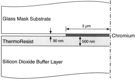
The basic model, shown in Figure 2-9, is a sandwich of four layers: glass mask substrate - metal layer - thermal polymer - Si0 2 buffer layer. The top and bottom
layers have enough thickness so as not to impact transient heating characteristics of the resist layer. In addition, the model is assumed symmetric about its centerline. This reduces computation time by a factor of two. The dimensions of the metal feature and the resist layer thickness are in agreement with the apparatus discussed in later sections. This allows the simulation results to serve as a guide in choosing the correct laser intensity and exposure duration in the actual experiments.
An adiabatic boundary condition was applied along all outer surfaces and along the axis of symmetry. This is justified because the time scales involved are extremely short and there is no time for appreciable thermal interaction with the surrounding environment. Laser heating was simulated as internal volumetric heat generation within the metal layer. This was accomplished by calculating transmitted optical energy and dividing by the mass of the metal feature.
In order to minimize the numerical precision errors that result from modeling small spatial dimensions and short time scales, the governing equations were
nondi-Glass Mask Substrate
3pm
-Chromium
ThermoResist ufe Ly90nm
Silicon Dioxide Buffer LayerI
Figure 2-9: 2D those from the
model used in ADINA finite element analysis. The dimensions match actual experiment
mensionalized and dimensionless versions of all necessary quantities were input into the ADINA model. In dimensionless form, equation (2.4) becomes:
Material 1: Material n: 0 0(
a(
a20 L 2 - + j9772 a,(pc)1(Tc - T) a 020 2_______ - n 026 L+c( a, 5r;2 + il(PC) n(Tc - Ti) T -T S Tc- Ti alt LcHere T is the initial temperature of the system, T, is some critical temperature of interest and L, is a characteristic length of the system. In the present analysis, T is taken as 20*C, Tc is 110'C, and Lc is 200 nm.
As indicated in equation (2.10), the diffusion equation for the first material is nondimensionalized using its own physical properties; subsequent materials are nondi-mensionalized with respect to the first material. This ensures that the relative
differ-31
where
ences between the various materials are preserved in the non-dimensional problem. When entering parameters into the finite element model, spatial dimensions were all given in terms of r and time steps in terms of (. The heat capacities for all materials were entered as 1 and the thermal conductivity for a material n as an/ai. Finally, the internal heat generation for the metal layer was modified by the appropriate factor shown in equation (2.10).
The model shown in Figure 2-9 was entered into ADINA and discretized into a standard mesh. An image of a typical mesh is shown in Figure 2-10. All results were computed at several mesh sizes to ensure convergence.
tZ
Line A Line B
X
Figure 2-10: A typical mesh used in simulation. Mesh size was varied for each com-putation to ensure convergence. Values at the nodes along lines A and B are used to study lateral heat flow
The model was subjected to internal heat generation in the metal layer and the resulting temperature contours were observed. As expected, in order to cure the resist through its thickness, there was an amount of lateral temperature spread roughly equal to the thickness of the resist layer. A typical temperature contour plot is shown in Figure 2-11. The scale is in the dimensionless temperature 0. This particular plot is a snapshot taken at t = 15psec and a heat flux of 5.1 x 10⁸ W/m 2. This corresponds
to an 8 W laser focused into a 100 pm spot at 50 % reflectivity. TEPBMTU .70 0W/W 01W A 224
Figure 2-11: Temperature contour plot at t=15 psec and a heat flux of 5.1 x 10⁸
W/M2
To gain more quantitative insight into the lateral temperature distribution, specific values are computed at the nodes along the top and bottom surfaces of the resist (lines
A and B shown in Figure 2-10). The time evolution of the lateral temperature profile
along the top and bottom surfaces is shown in Figure 2-12. In this particular case, the applied heat flux is 5.1 x 10⁸ W/m2. The solid curve depicts the profile at the
end of the exposure, and the two dashed lines show subsequent temperature profiles after heating has stopped. Decreasing the thermal capacitance of the system by using thinner metal and thinner resist layers will reduce post-exposure heat diffusion.
The effects of the incoming energy flux on temperature distribution are shown in Figure 2-13. The lateral temperature profile along the top surface of the resist is
shown for 3 different heat fluxes (5.1 x 10⁸ W/m 2, 1.3 x 10⁸ W/m 2, 5.7 x
107 W/m2)
that correspond to an 8 W laser at 50% transmittance focused into 100 /m, 200 pm, and 300 pm spots, respectively. Clearly, a higher flux produces sharper lateral temperature gradients. However, this benefit must be balanced with the accompa-nying larger temperature difference between the top and bottom resist surfaces. In order to cure the resist through its thickness the top surface must be substantially warmer than the bottom. Depending on the resist chemistry this may or may not cause problems at the top surface.
11-0~
E
a)
r0 1 2 3 4 5 6 7 8 9 10
Distance from centerline X ([tm)
Figure 2-12: Time evolution of the lateral temperature profile along the top and bottom resist surfaces. At t = 21 psec, heating is stopped and the temperature gradients soften. Along the top surface, the resist under the metal cools immediately while the resist adjacent to it increases in temperature. Along the bottom surface, temperatures increase everywhere as heat diffuses from the resist above.
The above results confirm that the primary means of increasing resolution is de-creasing the thickness of the thermoresist layer. To illustrate this point, a simulation was performed using a mask feature 200 nm wide and a resist thickness of 20 nm. The model is shown in Figure 2-14. The metal layer was subjected to a heat flux of 5 x 10' W/m2. A snapshot of the temperature profiles along the top and bottom resist surfaces at t = 180 nanoseconds is shown in Figure 2-15. As expected, the plot
appears qualitatively the same as Figure 2-12 - the only difference is the higher heat flux and shorter time scale. In this case lateral thermal diffusion is roughly 25 nm.
There is a great deal of uncertainty in the preceding analysis. The primary source is the material characteristics, and in particular the properties of the thermoresist. Generic polymer properties were used in modeling, but as discussed in Section 2.3.1, specific examples may vary widely in their thermal conductivities and in their behavior
300 I
-- t=21 [tsec (heat on)
250 -Resist Top Surface - - t=28.5 lsec (heat off)
200 . - - ... t=36 [tsec (heat off)
150-
--t
100 --
-
50--0 - -- -I
+-- Boundary of Mask Feature
140 - I
120- t - -Resist Bottom Surface
100 - - .
8 0 - - -
I I I I 1 200 , . - -~-150 C) -- = 5.7x0 m S 8 W/M2 q=5.1x1O W/m2 0 0 1 2 3 4 5 6 7 8 9 10
Distance from centerline ([tm)
Figure 2-13: The lateral temperature profile along the resist top surface (line A) for 3 different heat fluxes. Higher flux produces sharper temperature gradients and potentially better resolution.
at high temperatures. Many of these polymers were developed for specific purposes and have not been studied in the wide range of conditions necessary to produce accurate data. The type of glass used as a mask substrate has an impact as well, since a pure crystal such as quartz will have a conductivity an order of magnitude higher than ordinary glass. Also, the effects of thermal contact resistance at the metal-resist interface and thermal expansion were not considered. These should be examined in future work.
The lateral temperature distribution alone is not sufficient to determine the litho-graphic resolution. The contrast of the thermoresist is also necessary. In the lateral direction temperature varies smoothly from a peak value down to zero, and the chem-ical properties of the resist determine where the crosslinking cutoff occurs and how sharp it is. Unfortunately such information is not often available, and this introduces still more uncertainty into the picture.
35 %J&Ir I
Glass Mask Substrate
100nm
Chromium
Silicon Dioxide Buffer Layer
Figure 2-14: 2D model with reduced dimensions, illustrating the potential resolution of CTL. (D E U* 2C 15 1c E
Resist Top Surface t = 180 nanoseconds
q= 5 GW/m2
01
0 - - - -
-Boundary of Mask Feature 0
S-.. Resist Bottom Surface
... .. .. .... .. .. .0 ... ... . . .. . . . ... . .... .. . . .. . . o -. .. . .. ... ... .-.. --. ... -.. -.. ... .. .. .. .. . .. .... .. .-.. -.. ....-. - ... -- -... --... ---... to 0 100 200 300 400 500 600 700 800 900 1000
Distance from centerline X (nm)
Figure 2-15: The lateral temperature profile along the top and bottom resist surfaces at t =180 nanoseconds. Lateral thermal diffusion is roughly 25 nm.
Despite these limitations, the thermal and optical models presented here have some value. They provide order-of-magnitude estimates on key values such as optical intensity and exposure time and give valuable qualitative insight into the effects of changing variables such as exposure flux and resist thickness. This information was put to use in constructing a basic CTL system, the details of which are discussed in the next chapter.
Chapter 3
Experimental Setup
A basic CTL system was built to demonstrate the feasibility of the method. Time
constraints and a limited budget required that the system be made using easily ob-tainable parts and materials. The resulting apparatus and exposure method have very low throughput and are only capable of reproducing patterns on the order of a few microns. However, only a few basic changes would be necessary to increase both throughput and resolution.
The system can be broken into two main subsystems, an optics system and a wafer positioning system, plus a software scheme that ties the two together. The optics system includes a high power laser, a mechanism to create controlled short light pulses, lenses and mirrors. The pulse generator is a small scanning mirror which swings the beam through a wide arc. A thin slit positioned midway through the arc allows light through for a fraction of a second, and by varying the arc speed or slit width the pulse length can be controlled. The wafer positioning system consists of a vacuum wafer chuck to create intimate contact between the mask and wafer and a precisely controlled scanning stage to maneuver the wafer during exposure. Using custom software written in the LabVIEW environment, the two subsystems work together to characterize the incoming laser beam and to expose small regions of a silicon wafer coated with thermoresist.
An overview of the setup is shown in Figure 3-1. The details of the optics sub-system are described in the next section, followed by a description of the positioning
subsystem and LabVIEW control scheme. Finally, the choice of materials and mask design for the first tests is discussed.
Fixed Mirror facuum Fixture 532 nm Laser Scanning Mirror Slit Controlled Stage
LabVIEW Control System
Figure 3-1: Schematic of the basic CTL system. A scanning mirror swings the beam past a small slit, generating a controlled light pulse. The wafer and mask are held together on a vacuum chuck which is positioned by a computer-controlled stage.
3.1
Optics
The exposure laser used was a Millennia VIIIs continuous wave laser produced by Spectra-Physics. It contains an Nd:YVO4 doped crystalline matrix and can produce
up to 8 W of power in a continuous wave at 532 nm. The beam is Gaussian in profile and roughly 2 mm in diameter at full width half maximum. This wavelength was suitable for several reasons. Glass (both soda-lime and fused silica) are non-absorbing at 532 nm, it does not cause crosslinking in most polymers, and in common metals such as Cr, Al and Fe the 95% absorption depth is less than 30 nm.
Based on the numerical models presented in Chapter 2, the laser should heat the
sample for a duration between 1 psec and 100 psec. The low end of this range is too fast for mechanical shutters, so a scanning mirror system was implemented instead. The basic arrangement in shown in Figure 3-2.
Fixed Mirror
532 nm Laser
L =0.2 -1 mn
Lens
L = 0.1 - 10 deg Slit
Figure 3-2: Pulse generation system consisting of a scanning mirror and slit.
The scanning mirror used was Optical Scanner Model 6210 from Cambridge Tech-nologies, Inc. It consists of a 532 nm mirror mounted on a moving magnet motor. The mirror is capable of steering a 3 mm beam. The motor can produce large amounts of torque very quickly and thus has fast step response, on the order of 100 psec. An input signal is sent to the scanner's controller and the mirror responds by tracking the signal.
Two factors influence the pulse duration - the distance L between the mirror and the slit, and the angular speed of the mirror. In this setup, the distance L was used for gross control and the angular speed was used for fine control. The slit width was kept constant at 3 mm to allow the full beam through. A step input was sent to the scanner via the computer. The mirror swung from one end of its range to the other and the laser passed the slit midway between the two extremes. By controlling the size of the step impulse (and through that the angular excursion of the mirror), the peak speed can be adjusted for fine control. Figure 3-3 shows the relationship between angular excursion vs. pulse width for a distance L = 0.9 m. The pulse width at each
input level was measured using a fast photodiode connected to an oscilloscope. 41
40 35 -C)* 30 . .. C,, ~25- ~20-0) C,, =3 115-4-6 9 1 0
Angular Excursion (deg)
Figure 3-3: Pulse length as a function of angular step size as measured by a photodi-ode. The distance between the mirror and the slit is L = 0.9 m.
After the laser pulse passes through the slit, it is focused by a lens with a focal length of 5 cm. In order to determine the intensity at the mask surface, the focused beam diameter must be known. The beam was characterized by the simple method of slicing into the beam with a razor blade and recording the integrated intensity as a function of position. Differentiating this data produces a plot of the beam's intensity profile. A diagram of this scheme is shown in Figure 3-4.
The lens was mounted on a micro-positioning stage so that it could be moved parallel to the beam. By measuring the beam profile at several Z positions, the correct lens position for a desired spot size (and therefore intensity) could be determined. Figure 3-5 shows a typical beam profile that was captured. The smallest attainable profile with this lens/laser combination was around 10 ptm at full width half maximum. The depth of field of the lens was found by recording the spot size at several Z locations. This makes it possible to translate estimated errors in lens positioning
/ I Xt
Incoming Laser Beam
Figure 3-4: Beam profiling technique used to characterize the laser intensity at the mask surface. A computer records the integrated intensity at different positions and differentiates the results.
0 .0 4 5 - - - -- - - - - -.-.-- ----.- -.-.-.-.-.-.- .-- . -.-. -0 .-0 4 - - - -.-.-.-- -.-- - -.-.- -.-.-.-.- .- - .- .- . -0 .0 3 5 . . . .- - -. . . . .. . . . -. . -. . -.-.-.- -.-.-.- -.-- -.-.-- -.-.-.-.-.-.- - .- .- - - . Ca,3 0.03 - -.- - - - - -- - - - -0.025 - - -0 0 C 0 .0 1 5 - - - - --.- - - -.. . . . . -.. . .. . . . - -. . . .-- - - . . .- - - -. . . . .. . . -.- -.-- - - --. .- -0 .0 1 - ---. . . .- . . . . - - - - .. .. .-. . . . .- - -. .-.-.-.-.-. -. -. -.-. ---. -0 .0 0 5 - -.. . . . - - . . . . .. . . -. . . -. . . -.-.-.- -.-.-- -.- -.- -.-.- .- - .- .- .- - -. I I I I I 220 240 260 280 300 320 340 Blade X Position (stm)
Figure 3-5: A typical beam profile captured using the beam slicing method.
43
Photodiode
accuracy into errors in optical intensity. With the current system, the ability to place the wafer surface at the same plane as the razor blade is accurate to within roughly 500 pm. For a nominal beam diameter of 100 pum, a positional uncertainty of Z = ±500pum gives an uncertainty in optical intensity of ±40%.
3.2
Wafer Stage
The biggest mechanical challenge in implementing a CTL system is to maintain good thermal contact between the mask and the wafer over large areas. Fortunately, a number of solutions to the problem have been developed for use in other situations. The approach described here was developed for use in contact optical lithography and employs a thin, flexible mask that deforms to match the wafer surface. The general approach and mechanical designs were suggested by Dr. James Goodberlet.[16]
Figure 3-6 shows the vacuum fixture used to maintain intimate mask-wafer con-tact. The basic design is simple. Two thin metal plates, approximately 6" x6", sit on a 0.25" thick sheet of natural rubber. A standard 4" wafer and photomask are placed inside a square window cut in the two plates. On the bottom plate, a thin groove has been cut along the inside edge of the square window. The groove connects to a vacuum port and allows the air between the mask and wafer to be drawn out evenly from all sides. A close view of the bottom plate groove is shown in Figure
3-7. A rubber top layer covers the mask and wafer, sealing the top surface. The final
arrangement is shown in Figure 3-8.
With the top seal in place, a small roughing pump was connected to the vacuum port. Good mask-wafer contact is easily verified by inspection. Figure 3-9 is a pho-tograph of a mask and wafer under vacuum. Any dust particles are surrounded by colorful interference patterns commonly referred to as Newton's Rings. These are visible under ordinary white light, but are often more dramatic when viewed with a monochromatic source. The dark patches between the rings are regions of good contact.
Figure 3-6: Vacuum wafer fixture used to maintain intimate mask-wafer contact
Figure 3-7: A close view of the groove cut on the bottom plate. The groove allows air to be drawn out from between the mask and wafer.
Figure 3-8: Vacuum wafer with top seal in place.
Figure 3-9: Newton's rings between the mask and wafer under vacuum. On this dirty sample it is easy to see dust particles and dark regions of good contact.
Figure 3-10: Vacuum wafer assembly mounted on a motion stage. The stage was controlled by a LabVIEW program and moved in 0.1 pm increments.
as shown in Figure 3-10. The stage used was a Klinger CC1 and had a nominal step size of 0.1 Mm. Motion of the stage was controlled using LabVIEW software. The software synchronized the stage motion with the operation of the scanning mirror, enabling exposure of areas larger than the laser spot size.
3.3
Materials Selection
The most critical material for the CTL process is the thermoresist polymer. The type of polymer used determines the crosslinking temperature, resolution, edge sharpness and the resist layer thickness. Unfortunately, not many polymers have been studied with the purpose of local crosslinking in mind. For the vast majority of polymers, little data exists on thermal resolution or thermal contrast. In addition, as discussed in Section 2.3.1 bulk material properties such as thermal conductivity and heat capacity may change in very thin film configurations. Thus, choosing a polymer that is well suited to thermal lithography is challenging.
In order to avoid the difficulties of finding, testing and characterizing suitable resist polymers, an off-the-shelf solution was selected for initial testing. The polymer
chosen was a commercially available photoresist, AZ 5214-E (Clariant Corp), that has been optimized for image reversal. In normal image reversal lithography, selected portions of the wafer are exposed with UV light, generating an acid in the resist layer. The wafer is then heated in an oven, and the areas that contain acid crosslink and become insoluble. In CTL, the inverse of this approach is used: the wafer is flood-exposed with UV light, generating acid everywhere in the resist. Then, when the metal mask features are brought into contact and heated, local crosslinking occurs.
Using AZ 5214-E has several benefits. As a common optical resist, it is relatively well studied. The optical properties and crosslinking characteristics are known: it is transparent at 532 nm, and after exposure to UV light will crosslink at roughly
110 'C. It is approved for use in most clean rooms, and can be developed with
standard chemicals. Unfortunately detailed material property data is not available, so typical polymer properties are assumed. A more thorough investigation of the resist's properties should be undertaken in the future. The details of the process flow using this resist are presented in the next chapter.
The selection of the pattern mask is a much simpler job. The requirements are that the mask substrate be thin and optically transparent at 532 nm, and that the metal layer be strongly absorbing. A standard 4" chromium on glass mask meets these requirements. The substrate chosen for the first test masks was 0.020" soda lime glass, inexpensive and easily available. The masks were patterned with 90 nm of Cr in test patterns consisted of 8 pm gratings. Two variants were tried: an even pitch, with 8 pm Cr stripes and 8 pm spaces, and an every-other pitch, with 8 ptm Cr stripes and 16 pm spaces.
A standard 4" silicon wafer coated with 1.2 pm of SiO2 was used as a substrate.
The wafers were coated with AZ 5214-E and exposed at a variety of power levels. The detailed procedure and some results are presented next.