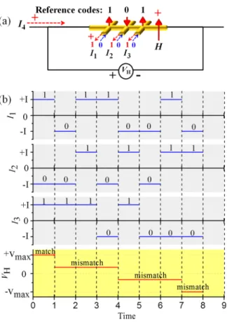
Extraordinary Hall effect based magnetic logic applications
Texte intégral
Figure
Documents relatifs
The first one is based on a explicit formula (see Theorem 3.1) obtained by the third author [12] for an isotropic composite with two isotropic phases, which immediately gives
In the case of the I-frame, the utility function is derived with respect to the individual contribution d i , and in the We-frame, all individual contributions d j are equal
Before presenting the example of an electrically isotropic composite having a negative Hall coef- ficient even though it is built from three phases each having a positive
But this time, it counts 9 parameters which are presented in Tab. The characteristic time τ is derived from the coefficient β in Eqn. It worths noting that the elastic
We have performed MC simulations of the magnetization at small values of the coupling constant for prismatic clusters corresponding to either well ordered (simple cubic, and c.f.c)
Other three relevant deontic logics based on non possible-world semantics are imperative logic (Hansen, 2008), prioritized default logic (Horty, 2012), and defeasible deontic
A brief review of some single-phase PLLs is made, then the proposed novel PLL structure is detailed and its performance is compared with that of the other PLL’s taking into
With these strengths, helicity has become widely applied to topics as diverse as magnetohydrodynamic ( MHD ) turbulence, magnetic dynamos, magnetic reconnection, turbulent relaxation
