Control of Morphology for Enhanced Electronic
Transport in PECVD-grown a-Si:H Thin Films
by
Sebastiin Castro Galnares
S.B. in Mechanical Engineering, Massachusetts Institute of
Technology (2008)
S.B. in Mathematics, Massachusetts Institute of Technology (2008)
Submitted to the Department of Mechanical Engineering
in partial fulfillment of the requirements for the degree
o
TMaster of Science in Mechanical Engineering
NOV
0
4 2
at the
MASSACHUSETTS INSTITUTE OF TECHNOLOGY~
ARCHIVES
September 2010
@
Massachusetts Institute of Technology 2010. All rights reserved.
Author...
... ...
Department of Mechanical Engineering
August 13, 2010
Certified by...
Tonio Buonassisi
Assistant Professor of Mechanical Engineering
Thesis Supervisor
Accepted by ...
David Hardt', Professor of Mechanical Engineering
Chairman, Department Committee on Graduate Theses
Control of Morphology for Enhanced Electronic Transport in
PECVD-grown a-Si:H Thin Films
by
Sebastian Castro Galnares
Submitted to the Department of Mechanical Engineering on August 13, 2010, in partial fulfillment of the
requirements for the degree of
Master of Science in Mechanical Engineering
Abstract
Solar cells have become an increasingly viable alternative to traditional, pollution causing power generation methods. Although crystalline silicon (c-Si) modules make up most of the market, thin films such as hydrogenated amorphous silicon (a-Si:H) are attractive for use in solar cell modules because of the capacity to fabricate cells with much less material. However, several challenges exist in making this material a more practical alternative to c-Si; despite having superior optical absorption properties, a-Si:H suffers in electronic transport, having a hole mobility 3-7 orders of magnitude less than that of c-Si.
In the MOSFET transistor industry, carrier speeds and thus mobilities of c-Si were improved through the application of stress in the material. This work hypothesizes that a similar application of stress on a-Si:H thin films can enhance this material's hole mobility. A comprehensive study of the parameter space for a plasma enhanced
chemical vapor deposition technique used to produce a-Si:H is performed. This
en-ables the control of stress within the deposited film, from compressive to tensile; the mechanical limits of the material resulting in buckling and delamination failure are observed.
Further characterization of a-Si:H thin films with different levels of engineered stress was performed; an analysis of the films' surface using AFM measurements to calculate a fractal dimension for each did not result in a significant descriptor of the surfaces' domain distribution.
This work includes a detailed analysis of the theory of time-of-flight for measuring carrier mobility in thin film materials, and the system requirements needed to perform them.
Thesis Supervisor: Tonio Buonassisi
Acknowledgements
Quiero
agradecer de todo coraz6n a mi familia. Pa, tu fuerza y tu sabiduria siempre han sido y seguirain siendo mi inspiraci6n. Ma, tu elegancia y pasi6n por la vida me han formado de una manera muy poderosa, y espero algiin dia poder tener aunque sea un poquito de tu espiritu. Nikki, eres dlnica. Eres la persona que mis admiro en este mundo; me iluminas, en todo el sentido de esa palabra. Sin mi familia no tengo nada, y los quiero mucho mis de lo que se pueden imaginar.Tonio, obrigado por ter acreditado em mim, mesmo nos momentos quando eu tinha deixado de acreditar em mim mesmo. Foi uma honra trabalhar com voc6, e posso dizer com orgulho que eu aprendi ao lado de alguem que vai mudar o mundo. Ndo tenho dd'vidas de que algum dia, nossos caminhos se cruzario novamente.
To all of my colleagues in the Labortory for Photovoltaic Research, I thank you immensely for these two years; through our research, but most importantly through your character and friendship, I have taken a small step towards bettering myself, both professionally and as a person.
Mariana, gracias por haberme cuidado y por brindarme una amistad tan bonita. Tu apoyo ha sido imprescindible en mi 6xito, y no s6 que hubiese sido de mi sin tu ayuda.
Finally, I would like to thank all of my collaborators at King Fahd University of Petroleum and Minerals. Your enthusiasm and knowledge for our project has been remarkable; your generosity, hospitality, and friendship a blessing. I am sure that this collaboration will only continue to grow and produce outstanding results.
Contents
Abstract . . . . Acknowledgements . List of Figures . . . List of Tables . . . . 1 Introduction . . . . 1.1 Energy consumption in the 2 1st century .1.2 Solar power . . . . 1.2.1 Solar resources . . . . 1.2.2 Photovoltaic technology . . . . .
1.3 The economics of PV . . . .
1.3.1 The Levelized Cost of Electricity 1.4 Basic photovoltaic conversion theory . .
1.4.1 Diffusion length . . . . 1.4.2 M obility . . . . 1.5 Amorphous silicon . . . . 1.5.1 Growth modes . . . . 1.5.2 1.5.3 1.5.4
Plasma Enhanced Chemical Vapor Deposition technology . Substrate selection and cleaning procedures . . . .
Experimental design and sample deposition . . . .
. . . . 17 . . . . 17 . . . . 19 . . . . 19 . . . . 20 . . . . 21 ... . 23 . . . . 24 . . . . 25 . . . . 26 . . . . 26 . . . . 27 29 30 31
. . . . 3 3
2.1 Types of stresses in thin films . . . . 2.1.1 Thermal stresses . . . . 2.1.2 Intrinsic stresses . . . . 2.1.3 Epitaxial stress (lattice mismatch) . .
2.1.4 Surface stress . . . .
2.1.5 Coalescence stress . . . .
2.1.6 Grain growth stress . . . .
2.2 Stoney's formula (Stress in a thin film) . . . . 2.3 Substrate curvature change measurements . .
2.4 Results of stress measurements on thin films conditions . . . .
for varying deposition
3 Fractal Dimension in Thin Films as a Proxy for Nanostructure . . . . 3.1 Introduction to fractals and fractals in nature . . . .
3.1.1 Defining fractals . . . .
3.2 Fractal dimension in a-Si:H as a proxy for nanostructure . . . .
3.2.1 Defining fractals on a thin film . . . . 3.2.2 Power Spectral Density (PSD) analysis . . . .
3.2.3 AFM imaging, data acquisition, and power spectra analysis . . 3.2.4 Results of fractal studies on thin films for varying deposition
conditions . . . .
4 Thin Film Spectroscopy for Thickness, Index of Refraction, and Density D eterm ination . . . . 4.1 Spectral reflectance measurements . . . . 4.1.1 Basic spectral reflectometry theory . . . . 4.1.2 Thickness and index of refraction mathematical modeling with
Kramers-Kronig relationship . . . . 4.2 Film density calculation . . . .
. . . . 33 . . . . 33 . . . . 35 . . . . 35 . . . . 35 . . . . 37 . . . . 38 . . . . 40 . . . . 44 45 49 49 50 52 52 54 55 57 63 63 63 65 66
2 Stress in Thin Films
.
4.2.1 Theory of film density calculation through Clausius-Mosotti m odel . . . . 4.2.2 FTIR for determination of thin film hydrogen content . . . . . 4.3 Results of film microstructure as a function of stress and deposition
conditions . . . .
5 Time-of-Flight for Mobility Measurements in an a-Si:H Thin Film . . . . . 5.1 Basic theory of Time-of-Flight . . . .
5.2 System design . . . . 5.2.1 RC-time constraints for a lumped-parameter TOF system model
5.2.2 Swept-charge physics and bias constraints from Hecht's Law .
5.2.3 Optical excitation constraints and ablation avoidance . . . . .
6 Conclusions and Future Work . . . ... 6.1 C onclusions . . . .
6.1.1 Stress modification through PECVD parameter variation . . . 6.1.2 Morphology characterization through AFM and applications of
fractal dim ension . . . .
6.1.3 Film densification and microstructure enhancement through the application of stress . . . .
6.2 Future w ork . . . .
6.2.1 Time-of-Flight measurements of hole mobility in a-Si:H . . . .
List of Figures
Fig. 1-1 Co 2 concentration in the atmosphere over the past millenium,
measured from air trapped in ice cores up to 1977 and then directly in Hawaii from 1958 onwards. The year 1769 is marked, as it saw the patenting of James Watt's steam engine. Note the exponential increase after this date; from [1] . . . . 18
Fig. 1-2 Historical and projected CO2 emissions through 2030; from [2] . 18
Fig. 1-3 Present and projected energy consumption in Quadrillion BTUs;
from [3] . . . .
19
Fig. 1-4 Schematic illustrating the power generating capacity of severalresources versus current generation need; from
[4]
. . . . 20Fig. 1-5 Diagram of a typical PV setup; from [5] . . . . 21
Fig. 1-6 Summary of the economics of a 1 MW, commercial installation in average irradiance fo 5 kW/m 2/day. Shows Compounded Annual Growth Rates (CAGR) of average grid retail price and average grid price for several PV technologies. Note that grid parity is achieved between 2014 and 2015; from [6] . . . . 22 Fig. 1-7 Schematic of electron-hole pair generation and charge separation
in a semiconductor pn junction; from [7] . . . . 24 Fig. 1-8 Comparison of absorption coefficients for various materials; from [8] 27 Fig. 1-9 Visual summary of thin film growth modes; (a) Volmer-Weber
is-land formation, (b) Frank-van der Merwe layer-by-layer and (c) Stranski-Krastanov layer-plus-island. 0 denotes amount of surface coverage; from [9] . . . . 28
Fig. 1-10 Simplified schematic of a PECVD system; from [10] . . . . 29
Fig. 2-1 Thermally induced stress calculation for a-Si:H film on c-Si substrate 34 Fig. 2-2 Diagram of film stress arising from lattice mismatch; gold material
is film while blue is substrate, redrawn from work [11] . . . . 36
Fig. 2-3 Thin film crystallite (gold) of thickness t and radius r deposited on substrate (blue) . . . . 37
Fig. 2-4 Wolmer-Weber growth islands coalescing. Stress is determined by a characteristic island radius . . . . 38
Fig. 2-5 Deposition process with surface adatoms filling a grain boundary and inducing a compressive stress o. The chemical potential of the free surface p, is greater than that of the grain boundary, ygb. 1(t) is the current film thickness as a function of time; from [12] . . . .-. . . . . 39
Fig. 2-6 Substrate with film applying a distributed line force
f;
detail shows a unit element being stressed in the radial and angular directions; from [13] . . . . 41 Fig. 2-7 Toho FLX system for substrate curvature measurement, rightimage shows sample on test bed . . . . 44 Fig. 2-8 Micrograph of film that failed from delamination . . . . 46 Fig. 2-9 Micrograph of films that failed from buckling . . . . 47 Fig. 2-10 Stress as a function of process pressure for the entire sample set 48 Fig. 3-1 Object M covered in N(6) cubes. The size of points comprising
M and cubes are varied in the figure to suggest depth, though they in
fact remain a constant size. Note that cubes can envelop multiple points 50 Fig. 3-2 Visual depiction of the Cantor set. Note that the structure is
scale-invariant . . . . 51
Fig. 3-3 Visualization of two surfaces with different morphological distri-butions, yet identical root-mean-square roughness R = A . . . . 53
Fig. 3-4 Typical 2 pm x 2 pm AFM scan; this film deposited at 600 mTorr and 20W , 200 nm thick . . . . 56
Fig. 3-5 PSD for a-Si:H AFM data with k-correlation fit; A = 1.5 x 10⁻⁹,
B = 8.33, C = 4.21 Note signal rise at high frequencies . . . . 57
Fig. 3-6 Fractal dimension as a function of process pressure . . . . 59
Fig. 3-7 Fractal dimension as a function of power . . . . 60
Fig. 3-8 Fractal dimension as a function of measured film stress . . . . . 61
Fig. 4-1 Schematic of basic spectral reflectance measurement . . . . 64
Fig. 4-2 Measured spectra for an a-Si:H thin film sample; Blue traces are the actual measurement and the initial guess for values of the index of refraction n, while red traces are the model fit for the spectra and index of refraction based on the Kramers-Kronig relation and user defined inputs ... ... 66
Fig. 4-3 Measured index of refraction n as a function of measured stress . 69 Fig. 4-4 Measured stress as a function of C x p, where C encompasses constants from the Clausius-Mosotti relation and the material's polar-izability. The grey lines are meant as a guide for the eye, showing first a linear decrease and then a constant value for stress over the range of the abscissa . . . . 70
Fig. 5-1 Typical a-Si:H sample architecture for hole mobility TOF . . . . 72
Fig. 5-2 System schematic of typical TOF setup . . . . 75
Fig. 5-3 Required time resolution curves for TOF mobility measurement. 76 Fig. 5-4 Percentage of swept charge for TOF setup as a function of applied voltage . . . . 78
Fig. 5-5 Absorption depth to typical depth ratio for various thin film m aterials[14-16] . . . . 80
List of Tables
Table 1.1 RCA clean summary indicating ratio of parts of each species for each step... ... 30
Table 1.2 Summary of base line PECVD recipe used to produce a-Si:H thin film sam ples . . . . 31
Table 2.1 Stress data summary . . . . 46 Table 3.1 Morphology and fractal dimension data . . . . 58
Chapter 1
Introduction
1.1
Energy consumption in the
2 1stcentury
Although many still dispute the impact of humanity's industrial activity on the Earth's resources and health, the available science has unequivocally demonstrated otherwise. Human energy consumption has become an issue of vital importance in as-suring the continued availability of natural resources, and the minimization of human-caused pollution that in turn impacts society's well being. Consider the growth of the greenhouse gas CO2 over the past millenium in Figure 1-1,
It should not strike anyone as a coincidence that the 1800s, seeing the birth of the In-dustrial Revolution, was the time period in which a marked increase in CO2 emissions
and atmospheric concentration was noted. But given the complexity of simulating the flow of greenhouse gases to and from the atmosphere, the research literature shows a certain disparity in what future emissions will be. However, there is widespread agree-ment that it will continue increasing, with some projections, such as the one shown in Figure 1-2 nearly doubling CO2 emissions for the year 2030 from 2000 levels, if no
concrete steps are taken towards abating emissions levels [2].
This rise in pollution is not surprising when considering the amounts of energy that humans use. Figure 1-3 shows present energy consumption and projected consump-tion through 2030. Despite a somewhat leveling off of energy demand from OECD (mostly developed) nations, the projected use from non-OECD nations, which include
200 25 -Do 0- 4 - ,'. ' AJM b 340 330" 280 \ 4 1000 1200 1400 1"00 100 2000
Figure 1-1: CO2 concentration in the atmosphere over the past millenium, measured from air trapped in ice cores up to 1977 and then directly in Hawaii from 1958 onwards. The year 1769 is marked, as it saw the patenting of James Watt's steam engine. Note the exponential increase after this date; from [1]
SUS. U am~da CMexxico OOECDU
4
0000-*12000
50
9)95 X) (X)5 2010 2015 220 2025 2
rapidly developing countries such as China and India, will rise substantially. Quatdridiion £Stu 400 200 0 2005 2010 2015 2020 2025 2G30
Figure 1-3: Present and projected energy consumption in Quadrillion BTUs; from [3]
1.2
Solar power
The sun's radiation provides a vast energy source for human consumption. There are several available and developing technologies which allow for the conversion of solar energy to other forms of energy. Solar thermal technologies use the sun's radiation to directly heat water or other liquid energy storage mediums, for either direct consump-tion or the generaconsump-tion of electricity through the producconsump-tion of steam. Solar hydrolysis
and Solar biodiesel use the sun's energy for the production of liquid and/or com-pressed fuels, H2 and methylated hydrocarbons, respectively. Photovoltaics convert
sun light directly into electricity, through the use of semiconductors.
1.2.1
Solar resources
The total amount of solar energy that is incident on the Earth is very large compared to most other resources. Consider below Fig. 1-4 detailing the availability of energy from different sources,
870 TW
86,000 TW
Wind
15 TW
32 TW
Global
Solar
Geothermal
Consumption
Figure 1-4: Schematic illustrating the power generating capacity of several resources versus current generation need; from [4]
Although much of the sun's solar resource cannot be directly harvested, it is still by far the largest available source on Earth, and is abundant enough to fulfill current and future power generation needs, many times over. This provides a strong, practical incentive to research photovoltaic and other solar energy harvesting technologies, such that they might be widely available and at an economically feasible price. By contributing no direct emissions, and requiring on average only a two year "payback" period on producing the amount of energy that was required to make it, photovoltaics could lead the way into a future where a significant amount of the world's energy needs are met by renewable sources, and the harm caused by human's reckless contamination and use of resources can be reversed.
1.2.2
Photovoltaic technology
Although two broader varieties of photovoltaics, crystalline silicon and thin films, exist, the basic concept behind all photovoltaic technologies is identical. The diagram below in Fig. 1-5 illustrates a typical PV setup.
AC outlets
DC ouWais
Figure 1-5: Diagram of a typical PV setup; from [5]
Sunlight impinging on a PV array is converted into electricity (see details of conversion in Section 1.4). The DC electricity generated is diverted to a charge controller which meters out the electricity to the various subsystems that are connected to the array. The charge controller also ensures that the power output is appropriately matched to all of the loads connected to the array. Some PV systems are connected to batteries which can store the generated energy for later use; however they are not necessary for the system to operate. Most PV systems also have an inverter; particularly for systems installed downstream where the generated electricity will be used in residential or commercial applications, an inverter is necessary to convert the electricity from the
DC to AC.
1.3
The economics of PV
The simplicity of use and environmental friendliness of PV systems have made these systems popular since their inception; however, the historically high cost of the en-ergy produced with a photovoltaic array has until recently prevented it from becoming a substantial percentage of both the national and global energy portofolio (usually expressed in cost per kilowatt hour, or $/kW - hr). Higher demand, better
manufac-turing techniques, as well as government subsidies, tax breaks, and incentives have all driven the price of photovoltaics down, to where in many markets it has already reached the average price of electricity in that market. This price equilibrium is called
grid parity. The last five years in particular have seen an average 60% growth rate in
the demand and sale of photovoltaics [17], despite a slowing-down of the market in
2009 from the world wide financial crisis and recession. Consider the below summary
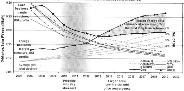
of the photovoltaic electricity market in Fig. 1-6.
1 MWp commercial installation (5kWlm21day solar irradiance) 0.30-- - -- -- ---- ---
---.margin
M 025 strctuje, - . ..
ROt profile sellng Ienergy on a
mmrcial scalle mady'offer
the best long tern returns 7%
-1 Proabitergrrsal * margin ndtstructure, ROc .. g d .s. 01kril- pi c-Sic(avoe)n
AV E. i- c-Si (hi C~j CdTe
A ra~gnd _____a-Si (ri) - GS
retail elecrcity oh c sfaM o rn inaveer r
0.05- T
20063 2007 2008 2009 2010 201 1 2012 2013 2014 2015 2016 2017 2018 2019 2020 Probable Larger scale
industry commercial gid
shakeout price, convergence
Figure 1-6: Summary of the economics of a 1 MWp commercial installation in average irradiance fo 5 kW/m 2/day. Shows Compounded Annual Growth Rates (CAGR) of
average grid retail price and average grid price for several PV technologies. Note that grid parity is achieved between 2014 and 2015; from [6]
Despite the recession in 2008-2009 and the removal of subsidies in large PV markets such as Spain, the price of PV-generated electricity has continued to fall. Not with-standing an approximately 20%-30% difference in generated electricity cost between crystalline silicon and thin-film technologies, it is likely that large-scale photovoltaic arrays will be able to achieve average-price grid parity between 2014 and 2015 in the
U.S. and other developed nations [6]. In order to appropriately analyze the
cost-benefit of a particular photovoltaic installation, the calculation of the levelized cost
of electricity gives the investor a simple estimate of how modifying one or several of
project.
1.3.1
The Levelized Cost of Electricity
An LCOE calculation allows for an investor to make generalized yet effective estimates as to the overall cost and profitability of a photovoltaic installation. In the simplest of terms for any energy-generating project, LCOE can be expressed as [18],
LCOE T l Total Life Cycle Cost
Total Lifetime Energy Production For the solar industry specifically, this can further be refined to,
Initial Investment -
Z
N DR" X (TR) + EN AC X (1 - TR)-LCO E = (1± _ n1 (1+ r)- (1 + r)n
N Initial k x(1 - SDR)n En=1 (1 + r)n
(1.2) Where r is the discount rate, DR is the depreciation rate, AC are the annual costs, TIR is the tax rate, RV is the residual value and SDR is the system degradation rate.
The indices n and N indicate a given year and the final year of a project, respectively
[18]. Note that by final year this analysis refers to the final year of financing; the
useful lifetime of photovoltaic systems are usually much longer than their financing periods (35-45 years versus 20-25 years respectively), making parameters such as the residual value and the system degradation rate very important in ensuring a low
LCOE. The technology innovation and geographical solar resource components of a
systems cost are reflected in the Initial kW*hr kWp term. Thus the equation reflects a clear aggregated benefit from research that both maximizes the useful energy produced by a solar array, and minimizes the cost of producing it.
In general, this simple LCOE model for the pricing of solar generated electricity can exemplify the sensitivity of price based on small changes in the input parame-ters of the photovoltaic system being designed. Although minimization of costs and maximization of energy production are in the broadest terms the best way to min-imize the cost of PV generated electricity, the LCOE highlights the importance of
sound strategic financing when designing a system for the cheapest possible energy production.
1.4
Basic photovoltaic conversion theory
Photovoltaic conversion begins with the interaction of a photon with a semiconductor material. Semiconductors (and in reality all materials) posess a property called the
band gap. The band gap is the amount of energy required to excite an electron from
the valence band to the conduction band. Consider the schematic of a photovoltaic process in Fig. 1-7 below, with band gap Eg,
hv
Figure 1-7: Schematic of electron-hole pair generation and charge separation in a semiconductor pn junction; from
[71
If an incident photon of energy hv has greater energy than the band gap, an
electron-hole pair is generated in the material. In order to separate the charges and have them contribute to the current through the device, a potential drop must be created within the device. To achieve this, photovoltaic devices are n-doped and p-doped, creating regions with excess electrons and holes respectively. The gradient in charge across the length of the device allows for charge separation; in particular the region between the doped layers, called the depletion region, acts to sweep the charges through the load connected to the device.
The transport properties of the material measure the facility with which carriers move through a semiconductor material. Note that depending on the doping of the material, it can have either excess electrons or excess holes; the carrier in excess is denoted the majority carrier, while the other is the minority carrier. Most transport properties can be measured for both, although the performance of a pn-junction-based solar cell is dictated by minority carrier transport properties. In some cases differ-ent techniques must be used to isolate the majority measuremdiffer-ent from the minority
measurement.
1.4.1
Diffusion length
The diffusion length of a carrier is defined as the distance that it travels before re-combining. Diffusion length must be maximized in order to ensure that the generated carriers reach the depletion layer of the PV device and thus being swept through the circuit and being harvested as useful energy. The diffusion length is written as,
Ld = V1r (1.3)
where D is the carrier's diffusivity in the material, and r is the carrier's lifetime. Lifetime is simply the amount of time that a carrier exists in the material before it recombines. Thusly by maximizing lifetime the distance the carrier is able to travel without recombining is maximized as well, allowing it to reach the depletion layer. A related concept is that of time-of-flight. Time-of-flight is the amount of time that it takes a carrier to traverse a certain distance within a device; in this work, that distance is from near one contact of a sample (where carriers are being generated) to the other, where they are swept through the circuit. Measuring the time-of-flight enables the calculation of another important transport property particularly important to the body of this work: carrier mobility.
1.4.2
Mobility
A carrier's mobility is a measure of how quickly it moves through a device with an
applied electric field (, such as those found in a photovoltaic device. The mobility y is defined as,
p = (1.4)
where vd is the carrier's drift velocity in the electric field. The current densities from electrons and holes Je and Jh can be estimated from the carrier mobilities through,
Je = gpn(1.5)
Jh = gpap( (1.6)
where n and p are the electron and hole densities in the conduction and valence bands, respectively. Mobility is affected by device parameters such as temperature, dopant species and concentration, and defect concentrations. In amorphous materials this last measure is particularly important, as the lack of an organized lattice provides a wealth of inherent scattering centers in the material. This both hampers the mobility
by increasing the likelihood of carriers colliding with atoms or defects, as well as that
of a recombination event which prevents the carrier from contributing to the device's circuit.
1.5
Amorphous silicon
There are several advantages to using amorphous silicon (a-Si) thin film solar cells as compared to crystalline silicon ones. In the visible spectra, a-Si is a much stronger absorber than c-Si. Below in Fig. 1-8 a comparison of the absorption coefficient for various thin film materials and c-Si.
10 G
10 1 Amorphous Siliconk/ YA I~I 1I; r
E Ci 1 0 ... 3 i 10 10 0 <10 200 400 600 800 1000 1200 1400 1600 1800 2000 2200 Wavelength, nm
Figure 1-8: Comparison of absorption coefficients for various materials; from [8]
device as compared to a c-Si one. The relatively low deposition temperature and this smaller energy inputs for a-Si fabrication as compared to c-Si also makes it attractive for use in lower cost photovoltaic devices.
Unfortunately, the defect-intense nature of a-Si gives it poor electrical transport properties. The mobility of carriers in a-Si, and in particular holes, is several orders of magnitude worse than that in c-Si; they can be as low as 1 x 10⁻³ V-S- [19]. As a result, a-Si devices exhibit much lower overall efficiencies than their c-Si counterparts, with a record efficiency of 9.5 ± 0.3% for a monojunction a-Si device [20].
1.5.1
Growth modes
Amorphous silicon, along with other semiconductor, metal, and non-metal thin films, are usually deposited onto a substrate through some kind of chemical vapor deposition
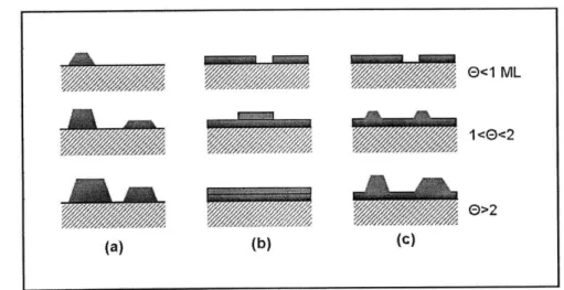
technique, in which a target material is either vaporized or already in gaseous form, and made to flow over a substrate. The material adatoms then attach to the substrate and eventually among themselves, build islands and layers. Most thin film growth can be characterized by three different growth modes. In Fig. 1-9 a visual summary of these modes is shown.
0<1 ML
/,~/~/~ / / 1<0<2
/ J f/J 4'/~ ' / ~ e>2
(a) (b) (C)
Figure 1-9: Visual summary of thin film growth modes; (a) Volmer-Weber island formation, (b) Frank-van der Merwe by-layer and (c) Stranski-Krastanov layer-plus-island.
E
denotes amount of surface coverage; from [9]Volmer-Weber growth results in the formation of island structures scattered about
the substrate surface. Most extremely thin films (thicnkess <1 nm) usually exhibit Volmer-Weber growth to some extent. For films that have a very high surface energy with respect to the substrate that they are being deposited on, Volmer-Weber growth
is usually the dominating growth mechanism.
In Frank-van der Merwe growth, smooth layers are built up one on top of the other. This growth mechanism is prevalent in film species with high self-affinity, and is characteristic of epitaxial growth techniques such as molecular beam epitaxy.
Stranski-Krastanov growth involves elements of both Volmer-Weber and Frank-van
der Merwe. Films that grow in this mode usually begin with several layers, and then begin to generate islands on top. Subsequent growth might continue islanding, but "filling-in" of the islands and observing subsequent layer-by-layer growth has been observed. Most real film deposition processes are more accurately portrayed by
Stranski-Krastanov growth than the other two growth modes.
1.5.2
Plasma Enhanced Chemical Vapor Deposition
technol-ogy
Most chemical vapor deposition techniques involve the vaporization or plasmification of a species to generate adatoms on the substrate surface. These adatoms then adhere to the surface and eachother, forming the actual material of the film. This study focuses on the use of Plasma Enhanced Chemical Vapor Deposition for the deposition of hydrogenated amorphous silicon samples (a-Si:H). Below in Fig. 1-10 a simple schematic of a PECVD system is shown.
top electrode 13J5M~z as inlet air4--chamber substrate to a water cooled to vacuum pump and pressure control valve
Figure 1-10: Simplified schematic of a PECVD system; from [10]
In a PECVD process, a gas or combination of gases is flowed into a process chamber over a substrate. The substrate sits on the bottom of an electrode, and another electrode hovers over the top of the sample. As the gas flows through the resultant space between the electrodes, and AC current or RF signal is used to generate a plasma of the gas mixture. In the plasma, several radical species form, of which some are adsorbed onto the substrate surface and become adatoms. Most PECVD tools have the ability to deposit at low frequencies (100s of kHz), high frequencies (13.56 MHz), or a mixture of both. Increasingly PECVD tools are the preffered choice for both research and industrial chemical vapor deposition: flow gases are easier to install than targets or hot wires, plasma enhancement allows for a much lower deposition
temperature and thus reduce the energy input into the system, and the ability to mix deposition frequencies allows for the control of stress and other film properties. This work uses a Surface Technology Systems PECVD for the deposition of a-Si:H.
1.5.3
Substrate selection and cleaning procedures
For this work, all samples were deposited on p-doped, 3" crystalline silicon substrates. The circular substrates allow for easy curvature change measurements, permitting the calculation of stress of films deposited on the surface. It was also chosen for flexibility in contacting; when a certain characterization technique required a direct contact, it can be evaporated directly on the c-Si surface prior to the deposition of the a-Si:H layer. Alternatively, if electric insulation is required, it is simple to deposit an oxide layer in between the substrate and the a-Si:H layer to accomplish this.
Substrate cleaning and preparation was accomplished through a typical RCA
clean, summarized below in Table 1.1,
Step name H20 2 NH4
0H I
Deionized H20 H2SO4[HF
RCA-1 1 1 Oxide strip 0 0 RCA-2 1 0 5 0 0 0 To necessary dilution 1 5 1 0
Table 1.1: RCA clean summary indicating ratio of parts of each species for each step
The above table shows the composition of chemicals used for each of the necessary steps. RCA-1 and RCA-2 are used to remove organic and metallic contaminants respectively; the samples should in these steps be placed into the mixture, at 75 'C for 10 minutes. It is recommended that the hot plate used should first be elevated to the necessary temperature, and to then pour in the necessary chemicals: failure to do so can result in an unwanted exothermic reaction, with vigorous bubbling spilling out of the chemical bath. RCA-2 is a particularly important step, as beyond its cleaning function, it also changes the surface states favorably for the deposition of a-Si:H and other thin films.
The oxide strip is used to remove the built up native oxide layer, and any contaminants within it. It is performed at room temperature, and a dipping time of one minute or
less is adequate with a sufficiently high percentage HF. Depending on the nature of the particular cleaning procedure desired, 10%-50% HF can be used
Between all steps, including after the RCA-2 step, the samples are placed in a quick
rinse of deionized water, and are submitted to at least 3 cycles, ensuring complete
removal of the chemicals used prior.
1.5.4
Experimental design and sample deposition
This work examines the modification of a-Si:H film properties through the induction of stress in the film. In particular, it is hypothesized that a-Si:H films'transport properties can be modified through the use of stress, similar to how the stressing of c-Si MOSFETs has augmented carrier mobility through the material, and thus allowing for faster transistor switching speeds [21].
To determine the effect that modifying the process conditions on a PECVD depo-sition of a-Si:H has on the level of film stress, and in turn how this stress affects film transport properties, a sample set of films was deposited on top of c-Si substrates. For the purpose of electrically isolating the film from the substrate, all samples had a 200 nm layer of silicon oxide deposited on its surface prior to a-Si:H deposition. Shown below in Table 1.2 is the base process recipe used for the generation of the
films,
Basic a-Si:H PECVD recipe
Temperature 200 0C
Flow rate SiH4 55 sccm
Flow rate Ar 0 sccm
Process pressure 200 mTorr
Power 20 W
Table 1.2: Summary of base line PECVD recipe used to produce a-Si:H thin film samples
From this basic recipe, several samples were deposited testing the extremes of each process condition, ensuring that for each, the film adhered to the substrate surface. Note that this does not necessarily imply that the films did not mechanically fail; part of this study characterizes the stress at which the films fail.
For the characterized batch of films, only process pressure and power were varied; large variations in these parameters still produced consistently wetted films, while still exhibiting variation in stress and other characterized properties. In the following sections, the range of variation in process pressure and power is discussed in more detail.
Chapter 2
Stress in Thin Films
2.1
Types of stresses in thin films
Mechanical stress in thin films arises from a modification in atomic positioning dur-ing film growth. By controlldur-ing the average distance from equilibrium that atomic position is changed, tensile and compressive stresses can be engineered into films [22]. Thus the stress in a film can be controlled, as well as its density. This work attempts to quantify the possible stress variation in a-Si:H films. The process conditions in the PECVD chamber used to deposit the films are systematically altered (See sec-tion 1.5.2-1.5.4 for detail). The process variables are temperature, process pressure, power, and film thickness. The stress conditions generated take the material through the extremes of possible stress states: from buckling failure, to compressive stress, to tensile stress and finally to delamination. Knowing the mechanical limits and the range of stresses which can be engineered into the films could be used to control the transport properties of the material.
2.1.1
Thermal stresses
Thermal stresses arise from the temperature differential the film experiences during growth and processing. A difference in the coefficient of thermal expansion (CTE) between the film and the substrate results in a larger contraction (or expansion) of
one material over the other, and thus inducing a stress. In Fig. 2-1, a calculation using published values for the CTE of a-Si:H [23] at different temperatures is used to estimate the amount of thermally induced stress for an a-Si:H film on a c-Si substrate.
5
0
-5
-10
-15
-20
300
400
500
Temperature [K]
Figure 2-1: Thermally induced stress calculation for a-Si:H film on c-Si substrate
The stress ut, as shown on the y-axis of Fig. 2-1, is calculated through,
-t= etMf Et = (a , - af)A T
(2.1) (2.2)
where et is the film strain, Mf is the film modulus, a, and af are the CTEs of the substrate and film, and AT is the temperature differential. The calculation reveals that in comparison to the intrinsic stresses locked into the film during growth (see data summary of intrinsic stresses for this study's samples in Table 2.1), the
thermal stresses do not contribute significantly for an a-Si:H thin film grown on a c-Si substrate. This is caused by th similarity of CTE for amorphous and crystalline silicon.
2.1.2
Intrinsic stresses
Intrinsic stresses is the general name for stresses that develop in a film during the growth stage. They can arise from a variety of mechanisms, of which the most important ones will be discussed in the following sections.
2.1.3
Epitaxial stress (lattice mismatch)
Epitaxial stresses arise from a lattice mismatch between the deposited film, and the substrate underneath. If the growth conditions are such that the creation of a per-fectly coherent interface [11] is possible, the film's lattice will align with that of the substrate; the larger the difference, the larger the stress. Figure 2-2 illustrates a typical lattice mismatch setup.
For a perfectly symmetrical case, the epitaxial stress o-e can be calculated by,
'e= CeMf (2.3)
a. - af
1e - af (2.4)
af
where a, and af are the substrate and film lattice constants, respectively.
2.1.4
Surface stress
Surface stresses arise from the amount of reversible work required to create a surface area A. The total amount of work needed to create a surface is given by,
Figure 2-2: Diagram of film stress arising from lattice mismatch; gold material is film while blue is substrate, redrawn from work [11]
where -y is the surface energy of the material. Surface stresses are the predominant contributor of intrinsic stress for films that have at least one dimension less than 10 nm
[24].
Consider a schematic of a thin film crystallite under surface stresses, in Figure 2-3.With a small island-like structure such as the one depicted in Fig. 2-3, the surface stresses on the top, side walls, and interface with the substrate can be used to express the total strain er the element experiences under equilibrium[11],
1 Ff-ihgl
S=
1
h+ -
(2.6)
My t r
where
f,
g, and h are the surface stresses of the top, sidewall, and interface stressesFigure 2-3: Thin film crystallite (gold) of thickness t and radius r deposited on substrate (blue)
2.1.5
Coalescence stress
Recall from section 1.5.1 the Volmer-Weber mechanism of film growth: adatoms on the substrate surface agglomerate to form islands of material distributed over the substrate surface. Once islands begin to impinge on each other (called the percolation
point), they coalesce into grains and grain boundaries, and stresses arise from the
input of material into the now closed space between these islands.
Consider below in Fig. 2-4 a network of film islands transitioning into coalescence. Note that though the islands here are shown as spherical caps (and are a good ap-proximation of morphology observed for a-Si:H thin films), films can exhibit a variety of Volmer-Weber island shapes.
Following the analysis of [13], for a characteristic island of radius R, the average stress that develops from coalescing islands on a substrate surface is given by,
1-ave =0.44 E (2.7)
Rs
con-Figure 2-4: Wolmer-Weber growth islands coalescing. Stress is determined by a characteristic island radius
dition
[25].
Slower depositions tend to form larger crystallite islands before reaching the percolation point, and thus result in lower coalescence stresses.2.1.6
Grain growth stress
Stresses can develop in a film with the development of grain boundaries, and in particular when they are incorporated in the material bulk [11]. In general, grain boundaries are less dense than the bulk material, meaning that their annihilation leads to increased film density and thus film stress. There are several mechanisms for stress changes associated with grain boundary modification, which can lead to both tensile and compressive stresses.
Consider a film with average grain size LO and an excess volume per unit of grain boundary Aa. If the film grains are allowed to grow to a size L (for example through
an annealing procedure), the volumetric strain is given as,
AV = 3Aa (- ) (2.8)
(L Lo This results in in-plane strains given by,
10 1
fe = Aa (2.9)
( Lo L
-g= MfAa (
)
(2.10)(Lo L
Another important mechanism for stress arising from the growth of grains is the filling of grain apertures with flux adatoms from the PECVD or sputtering procedure [12]. Consider a film/substrate system such as the one below in Fig. 2-5, where u(y) is the width of the layer of material at a particular point y along the axis of the grain boundary.
Deposition flux
-4- e
Filml
Figure 2-5: Deposition process with surface adatoms filling a grain boundary and inducing a compressive stress o-. The chemical potential of the free surface p, is greater than that of the grain boundary, pgb. l(t) is the current film thickness as a function of time; from [12]
A simple linear spring model for the stress developed in a grain boundary crack is
given by,
U(Y) cgb(Y)
(2.11)
w Mf
where w is the grain width and Mf is the film elastic modulus. A gradient in the chemical potential p, and pgb, of the surface and grain boundary respectively, causes the adatoms concentrated on the surface to fill in the gap of the grain boundary. If F is the jump rate of adatoms into the grain boundary, and is a function of an activation
barrier AG* for incorporating the adatom into the grain boundary wall's material, the evolution of the stress in the grain boundary can be written as,
00 11t 2CemQ2/3
(C JD _ [o- u (l, t)] (2.12)
where C. is the concentration of adatoms on the surface, Q is the atomic volume, D is the grain boundary diffusivity, and 6 is the thickness of a layer in which interface diffusion is supposed to take place. The quantity a, is a constant representing the steady-state grain boundary stress if the grain boundary and free surface reached equilibrium during deposition [12]. Note that this description of stress is strictly the normal, localized stress at the point y on the grain boundary. A further relation is needed to relate this quantity to the overall stress of the film. If the average grain boundary stress is given by rave, the change in the product of stress and thickness
(also called the line force) given in several experimental results can be written as,
A(ol), = A [o-avel(41/w) tanh(w/4)] (2.13)
2.2
Stoney's formula (Stress in a thin film)
Because thin films are usually several orders of magnitude thinner than the substrates that they are deposited on, stresses induced by thin film deposition are usually con-sidered to be constant throughout the entire thickness of the thin film. The observed curvature change after film deposition can be used with Stoney's formula to calculate the stress in the film. The following derivation is based on work presented in [13] and the substrate-film system used for the derivation is shown in Fig. 2-6.
Several assumptions are needed for the proper derivation of the formula. First, the distributed line force and the deformation it induces are assumed to be axially symmetric, implying that all stress states are independent of 0 in the selected coordi-nate system. Second, the distributed line force
f
induces a plane stress state, and any nonlinear effects towards the edges of the bi-layer are ignored. Finally, the substrate's midplane is assumed to deform through an isotropic strain, and its curvature isuni-Figure 2-6: Substrate with film applying a distributed line force
f;
detail shows a unit element being stressed in the radial and angular directions; from [13]form (resulting in an overall spherical deformation). Summarizing these assumptions in terms of the stresses and strains of the selected coordinate system:
o-22= 0 (2.14)
Cro = 6rz =
0 (2.15)
COO(r, 0) = Err (T, 0) = CO (2.16)
The complete stress state of the deformation can be expressed as a function of the Lame constants with the following tensor:
-rr 2p + A A A Err
000 A 2- + A A E00 (2.17)
0 A A 2p, + A E22
The Lame constants y and A are functions of the Young's Modulus E (sometimes denoted Elastic Modulus) and the Poisson's ratio v of the substrate material,
E
yE (2.18)
2(1 - 2v)
A = (2.19)
The stress induced by a deposition process in the thin film can be derived from the overall energy that is derived from this process in deflecting the substrate. The following expression describes the total energy density of the substrate, in terms of the perceived stresses and strains in each of the coordinate directions, and the appropriate material properties:
P=
>'
=: 2(1 + v)(1 - v) [ 2 +dE
+ 2verreO] (2.20)Note that strains can be written in terms of unit cell displacements in the coordinate directions. Let u, v, and w represent displacements in the r, 0, and z directions respectively. The non-zero strains in the deformed substrate can be written in terms of these displacements and their derivatives as follows:
Err(rz) = it(r) - zd)(r) (2.21)
- u(r, - -b(r) (2.22)
r r
The displacements in turn, can be written parametrically such that the expression for the displacement of the material is expressed only in terms of the material's mechanical properties, the induced isotropic strain and constant curvature EO and K respectively, and the coordinate r, namely:
u(r) = cor (2.23)
w(r) = (r2 2.24)
2
If we input these parametric expressions and their derivatives into the equations for
strain, we can re-write the energy density of the deflected substrate as,
where M, is the substrate's biaxial elastic modulus, defined as,
MS E (2.26)
1- v
The total potential energy in the deformed substrate is the sum of energies con-tributed from the intrinsic deformation of the substrate and that concon-tributed by the deposition induced distributed line force
f.
If we consider a substrate with radius 0 to R on the r axis, angular rotation of 0 to 27r on the 0 axis, and extension -h,/2 to h,/2on the z axis (with the magnitude h, defining the total thickness of the substrate), the expression for the total potential energy is as follows:
V(, K)= 2-rj jh/2 p(r, z) - r -dzdr + 27rR2f
-p(R, h,)
0 --h /2 11( .7
rR2Mshs eo+
K2±h2 + 2wR2f 60 - sh)
Once a film has been deposited on the substrate, determining the stress in the film through the total potential energy is a matter of considering the parameters that make the total potential energy stationary, vis-d-vis,
-V -OV - 0
(2.28)
&0 O3K
At a stationary total potential energy, the above can be solved to yield the midplane strain E0 and the curvature ,
EO = (2.29)
Mohs
K = 6f (2.30)
Ms h2
Referring back to the key assumption of the film being much thinner than the sub-strates they are deposited on, the induced stress in the thin film is constant throughout its thickness, thus a mean stress can be determined with,
om = - (2.31) hf
where hf is the thickness of the deposited film. Finally, inputting the appropriate expression for
f
from the curvature K yields Stoney's formula,M,h 2
-m = 8 (2.32)
6h5
2.3
Substrate curvature change measurements
The stress of the sample set described in Section 1.5.4 was measured through changes in substrate curvature before and after thin film deposition, as described previously through Stoney's formula. The measurement was performed in a Toho FLX-2320-S thin film stress measurement system. The system is shown in Fig. 2-7, together with a sample on the instrument's test bed.
Figure 2-7: Toho FLX system for substrate curvature measurement, right image shows sample on test bed
The measurement is performed by rastering a laser over an axis on the sample's surface; an optical detector receives the reflected laser beam and interpolates changes in angle as the shape of the substrate surface. The software then calculates a ra-dius of curvature based on the detected profile. For best results with the tool, it is recommended to exclude the edges of the samples; for the 76.2 mm c-Si substrates
being used, only the inner 60 mm of each were measured. A measurement is taken before the film is deposited, and one is taken after. With these two measurements, the change in curvature K can be calculated through,
S= 1 (2.33)
R Ro
where R is the substrate's post-deposition radius of curvature, and Ro is the radius of curvature before deposition. It should be noted that although it was not used for this study, this system is capable of temperature dependent measurement in the range of
-65 0C to 500 OC; this allows for the calculation of biaxial modulus and coefficient
of thermal expansion for novel materials.
2.4
Results of stress measurements on thin films
for varying deposition conditions
Stress was measured for a sample set which included films deposited at different power and pressure. Different thickness films were also deposited; for the submicron thickness range, thickness variation did not significantly impact stress, and is further discussed in Chapter 4. Stress data for the sample set is shown in Table 2.1. Note that several other films are not listed because they exhibited some failure mechanism, invalidating any curvature change measurement for the calculation of stress.
The objective of this study was to investigate the effect of changes in the PECVD chamber conditions on stress; in particular process pressure and power. Both tensile and compressive stresses were engineered and the parameter space was studied until the a-Si:H films reached mechanical failure. Shown in Figs. 2-8 and 2-9 are micro-graphs of the films in tensile and compressive failure modes, denoted delamination
and buckling, respectively.
The a-Si:H samples were engineered to stresses that ranged from about -1000 MPa to 400 MPA. By extrapolating to the stress measured in the process conditions closest to where films were found to fail, the buckling stress and delamination stress were
Sample ID Power [W] Process pressure [mTorr] Stress [MPa] W01 30 100 -910.6 W03 30 100 -983.4 W12 20 600 340.5 W13 30 600 343.2 W14 35 200 -605.5 W15 35 600 343.1 W16 20 600 324.1 W17 30 600 377.1 W18 20 200 -422.1 W19 30 200 -563.9 W20 30 200 -462.3 W21 35 200 -605.4 W22 20 200 -406.1 W23 30 400 168.0 W24 30 800 387.4 W25 35 600 355.1
Table 2.1: Stress data summary
Figure 2-8: Micrograph of film that failed from delamination
estimated to be -1200 MPa and 450 MPa, respectively.
Power was found to not have a significant effect on the stress; at identical power conditions, stress varied on average only by 10.5%, which was consistent with the
Figure 2-9: Micrograph of films that failed from buckling
measurement error in curvature over all samples.
Pressure was found to be a powerful method of adjusting the stresses in the deposited film. The compressive values are consistent with what has been reported in the literature previously [25]. This study is novel in that it used a large pressure range of
100 - 1000 mTorr to show a transition from compressive to tensile stresses in a-Si:H. Figure 2-10 shows the evolution of stress in a-Si:H over this range. Note that data points for 1000 mTorr are not shown because all of the films deposited at this pressure failed and delaminated.
Increase of process pressure in other studies has been shown to exhibit changes in stress from compressive to tensile regimes [16], much like that observed in this study. This phenomenon is thought to arise from the increased collisions between plasma and gas molecules under increased pressure; this results in less plasma molecules impinging on the surface of the substrate and densifying into a film [16]. Less dense films are thus composed of atoms that are more spread out in their amorphous matrix, and farther away from an equilibrium position. Note that the 800 mTorr films show roughly the same amount of stress as the 600 mTorr and 1000 mTorr films; however,
Delamination failure 400
200Tensile
stress
0 -200 - -400 _Compressive
stress
S-600 .. ____S-800
1..~~ -1000 Buckling failure -1200 -- -- - - --- ------0
200
400
600
800
1000
1200
Process pressure [mTorr]
Figure 2-10: Stress as a function of process pressure for the entire sample set
Chapter 3
Fractal Dimension in Thin Films as
a Proxy for Nanostructure
3.1
Introduction to fractals and fractals in nature
First described formally in Benoit Mandelbrot's seminal work in 1975 [261, fractals are geometric shapes exhibiting complex branch-like structures which are difficult to describe with regular Euclidean geometry, and that have the non-intuitive property of being characterized by a dimension that is usually non-integer. What sets fractal structures apart from other families of irregular or fragmented structures is that they exhibit the property of self similarity . Self similar objects are those that resemble themselves at varying scales of magnification. These can further be divided into
scale-invariant objects and self-affine ones. Scale invariance describes objects that resemble
themselves exactly in all spatial directions for which the object is defined and can be either statistically invariant or exactly invariant, the former denoting invariance over a range of scales and the latter that the object resembles itself over all scales. Self-affine objects are those whose similarity is scaled by different amounts in differ-ent spatial directions. Although typically associated with mathematical abstraction (and many famous fractal structures, such as the Burning ship fractal , are defined mathematically), fractals can be appreciated in all sorts of natural systems, such as clouds, mountains, and coastlines. There is a wealth of research into the use of

![Figure 1-3: Present and projected energy consumption in Quadrillion BTUs; from [3]](https://thumb-eu.123doks.com/thumbv2/123doknet/14479372.523781/19.918.273.654.201.468/figure-present-projected-energy-consumption-quadrillion-btus.webp)
![Figure 1-4: Schematic illustrating the power generating capacity of several resources versus current generation need; from [4]](https://thumb-eu.123doks.com/thumbv2/123doknet/14479372.523781/20.918.115.773.130.518/figure-schematic-illustrating-generating-capacity-resources-current-generation.webp)
![Figure 1-5: Diagram of a typical PV setup; from [5]](https://thumb-eu.123doks.com/thumbv2/123doknet/14479372.523781/21.918.220.695.117.413/figure-diagram-typical-pv-setup.webp)

![Figure 1-8: Comparison of absorption coefficients for various materials; from [8]](https://thumb-eu.123doks.com/thumbv2/123doknet/14479372.523781/27.918.151.780.106.609/figure-comparison-absorption-coefficients-various-materials.webp)

![Figure 2-2: Diagram of film stress arising from lattice mismatch; gold material is film while blue is substrate, redrawn from work [11]](https://thumb-eu.123doks.com/thumbv2/123doknet/14479372.523781/36.918.155.785.182.553/figure-diagram-arising-lattice-mismatch-material-substrate-redrawn.webp)
