HAL Id: hal-01764916
https://hal.archives-ouvertes.fr/hal-01764916
Submitted on 4 Jul 2018
HAL is a multi-disciplinary open access
archive for the deposit and dissemination of
sci-entific research documents, whether they are
pub-lished or not. The documents may come from
teaching and research institutions in France or
abroad, or from public or private research centers.
L’archive ouverte pluridisciplinaire HAL, est
destinée au dépôt et à la diffusion de documents
scientifiques de niveau recherche, publiés ou non,
émanant des établissements d’enseignement et de
recherche français ou étrangers, des laboratoires
publics ou privés.
Terahertz HgTe Nanocrystals: Beyond Confinement
Nicolas Goubet, Amardeep Jagtap, Clément Livache, Bertille Martinez, Hervé
Portalès, Xiang Zhen Xu, Ricardo Lobo, Benoit Dubertret, Emmanuel
Lhuillier
To cite this version:
Nicolas Goubet, Amardeep Jagtap, Clément Livache, Bertille Martinez, Hervé Portalès, et al..
Tera-hertz HgTe Nanocrystals: Beyond Confinement. Journal of the American Chemical Society, American
Chemical Society, 2018, 140 (15), pp.5033-5036. �10.1021/jacs.8b02039�. �hal-01764916�
TeraHertz HgTe nanocrystals: beyond confinement
Nicolas Goubet
1,2,3,
Amardeep Jagtap
1, Clément Livache
1,2,3, Bertille Martinez
1,2,3, Hervé Portalès
4,
Xiang Zhen Xu
2,3, Ricardo P.S.M. Lobo
2,3, Benoit Dubertret
2,3, Emmanuel Lhuillier
1*1Sorbonne Université, CNRS, Institut des NanoSciences de Paris, INSP, F-75005 Paris, France 2 LPEM, ESPCI Paris, PSL University, CNRS, F-75005 Paris, France
3 Sorbonne Université, CNRS, LPEM, F-75005 Paris, France
4 Sorbonne Universités, UPMC Univ Paris 06, CNRS, UMR 8233, MONARIS, 4 Place Jussieu, 75005 Paris, France
Supporting Information Placeholder
ABSTRACT: We report the synthesis of nanocrystals with optical
feature in the THz range. To do so, we develop a new synthetic procedure for the growth of HgTe, HgSe and HgS nanocrystals, with strong size tunability from 5 nm to 200 nm. This is used to tune the absorption of the nanocrystal all over the infrared range up to the teraHertz (from 2 µm to 65 µm for absorption peak and even 200 µm for cut-off wavelength). The interest for this procedure is not limited to large size since for small objects we demonstrate low aggregation, good shape control (i.e. spherical object) while using non-expansive and simple mercury halogenide precursors. By inte-grating these nanocrystals into an electrolyte-gated transistor, we evidence a change of carrier density from p-doped to n-doped as the confinement is vanishing.
Colloidal quantum dots (CQD) have garnered significant scientific and technological interests because of their tunable optical features from ultraviolet (UV) to infrared (IR). While their photolumines-cence appears as the first mass market application, CQD are actu-ally as interesting for the design of low cost optoelectronic devices that combine the ease of processing of solution-processable mate-rial with the robustness of inorganic systems. This is especially true in the IR range where current technologies remain pricy. CQD offer an interesting platform, however reaching mid (λ>3 µm) and far infrared wavelength is challenging on a material perspective.1–3
Only few materials can address absorption tunability up to the te-rahertz range: graphene4, doped semiconductors (Si, InSb)5,6 and
topological insulators such as Bi2Se37. However, the strong field
localization of terahertz plasmon in a subwavelength volume makes that materials need to be designed in gratings. The wet chemical synthesis can be a potential alternative and easy way to produce terahertz materials. To reach this goal, the current syn-thetic procedures need to be pushed toward CQD-based terahertz technology. Mercury chalcogenides (HgX: HgS,8,9 HgSe10–12 and
HgTe13) have reached the highest maturity to address this part of
the electromagnetic spectrum because they combine mid-IR tuna-ble optical features with photoconduction. Lots of effort have been made for the integration of HgX CQD, including the design of pho-toconductive14,15, photovoltaic,16 phototransistor, devices17,
plas-mon assisted photodetection,18–20 multicolor detection21,22 and even
hybrid with graphene23,24. A recent review on the field is given in
ref 25.
Among HgX, HgTe is the compound that leads to the best perfor-mances, with the lowest dark current and the fastest time re-sponse.25 However, the current state of the art synthesis for mid-IR
HgTe CQD relies on Keuleyan et al. synthesis and keep suffering from several limitations, which are discussed in more details in the supporting information.26,27 In particular the material grows with
an anisotropic shape (tetrapod or tetrahedron, see figure S1-S4) which tends to self-assemble into pairs (see figure S4) and leads to a loss of colloidal stability even for moderate size CQD. This is extremely detrimental to the design of pinhole free layer for vertical geometry device. Moreover, the final objects are strongly faceted and present the least reactive facet, which is limiting for growth of heterostructures. This perspective is even more challenging due to the high reactivity of mercury with chalcogenides. Consequently, nucleation and growth steps are difficult to be time-separated and low temperature growth is used in current synthesis (60-120°C), making the obtained material incompatible with usual high temper-ature (200-300°C) growth process of wide band gap colloidal ma-terial.8,28 In term of shape control HgTe has not yet reached the
ma-turity of CdSe. 2D HgTe platelets have recently been proposed by Izquierdo et al.29 but they remain limited to the near-IR range. Shen
et al30 have also proposed the use of a more reactive precursor such
as bis-(trimethylsilyl)telluride (TMSTe) as a way to improve sphe-ricity and aggregation. However, TMSTe is expensive and has a very limited stability, which prevents such synthesis to be viable at least at the industrial scale. Last, the current range of size spans from 3 to 20 nm, which makes that the obtained material is still strongly confined since HgTe presents a large exciton Bohr radius of 40 nm.31 This prevents current material to address wavelengths
above 12 µm27,32 and also limits the emergence of topologically
protected states which are expected for poorly confined objects.33,34
In this paper, we report a new and simple synthetic procedure for the growth of HgTe CQD. We demonstrate size control from 5 nm to above 200 nm, which allows for the first time to cover the whole infrared range from 2 µm up to the THz range (65 µm) with a single material. In particular, we focus on long wavelengths (10-100 µm range), which are non-addressable based on previously reported synthesis. We also integrate these materials into electrolyte-gated transistors and demonstrate that HgTe CQD switch from p-type for the smallest size to n-type for the largest CQD.
To achieve a higher degree of control on HgTe CQD synthesis, we investigate for less reactive precursors. Our approach is based on the simultaneous injection of HgX2 (with X=Cl, Br or I) and Te
oleylamine. It is worth noting that the procedure can be extended to the growth of HgSe and HgS (see figure S9 and S10), while using NaBH4 reduced Se and elemental sulfur in oleylamine,
respec-tively.
Figure 1. (a). absorption spectra of HgTe CQD with various sizes.
(b) absorption spectra of HgTe CQD with various sizes, presenting a plasmonic feature in the LWIR, VLWIR or THz range. (c) Cut off wavelength of the interband transition (for material without plasmonic feature) and plasmonic peak wavelength (for doped ma-terial) as a function of the CQD size (diameter for spherical object). SWIR corresponds to Short-Wavelength Infrared range (1.5 to 3 µm), MWIR to Mid-Wavelength Infrared range (3 to 8 µm), LWIR to Long-Wavelength Infrared range (8 to 12 µm), and VLWIR to Very Long-Wavelength Infrared range (12 to 30 µm). Inset: full width at half maximum (FWHM) of intraband peak as function CQD size.
The size of the CQD is driven by three key parameters, which are temperature, the reaction time and the chosen mercury halide pre-cursor. By tuning the reaction temperature from 120 °C up to 340 °C, the mean size of the CQD can be tuned from 5 nm up to 200 nm, see Figure 1c, 2 and Figure S5. Thus, it is possible to obtain absorption all over the infrared range from 2 µm up to 65 µm, see
Figure 1. This approach presents the key advantages to both be
able to synthesize small CQD sizes with sharp excitonic transition, but is also well suited to obtain large CQD, which are able to ad-dress long wavelength (>12 µm). Figure 1b shows how the Wavelength Infrared range (LWIR, 8-12 µm range), Very Long-Wavelength Infrared range (VLWIR, 12-20 µm range) and THz (λ>30 µm) can be finely addressed using the developed protocol. The optical features have been pushed to an energy typically twice smaller than the previous record.10
In the case of large CQD, the spectrum is made of two components: an interband absorption at high energy and an intraband/plasmonic peak at low energy, see Figure 1a and b. The exact nature of the long wavelength feature actually depends on particle size and dop-ing level.8 The energy of this transition can be made low enough,
so that the peak overlaps with the absorption resulting from the LO phonon line (at 123 cm-1). The Raman spectrum in figure S11
con-firms the phonon character of this line. Another striking behavior is the exceptional narrowness of the intraband/plasmonic peak (< 200 cm-1) compared to what it can be for doped nanocrystals of Si35
or oxides36–38 (with a FWHM >1000 cm-1).
While the role of reaction time is rather trivial with an increase of the final size with time, the role of halide is more complex. We observe that chloride leads to larger objects compare to the other halides (>Br>I), see Figure 2. This trend is confirmed by following the absorption of the solution at 415 nm, which is the signature of
the amount of crystalline HgTe, see figure S5.32 Even at low
tem-perature (120 °C), the reaction is almost complete after 3 min in the case of HgCl2, while it is still unfinished after 3 h while using HgI2.
As shown in Figure 2a, d and e, iodine precursor leads to more fac-eted objects. This may be attributed to the soft base character of iodine that allow a better bonding and poisoning surface made of soft acid mercury.39
As recently proposed by Shen et al,30 it is possible to tune the
mag-nitude of the long wavelength peak of the absorption spectra while tuning the reaction stoichiometry. For moderate size CQD (12-40 nm), only the interband contribution is observed in the case of stoi-chiometric reaction (Hg:Te=1:1), while the long wavelength fea-ture is obtained in Hg rich condition, see figure S8. Hg rich material tends to be n-type doped, which favor the observation of the intra-band/plasmonic feature as observed for HgS and HgSe which are intrinsically n-doped.40
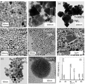
Figure 2 (a), (b) and (c) are Transmission Electron Microscopy
(TEM) images of HgTe CQD synthetized at 180°C with HgI2,
HgBr2 and HgCl2 as Hg precursor, respectively. (d) and (e) are
TEM images of HgTe CQD synthetized using HgI2 as precursor at
250°C and 300°C, respectively. (f) and (g) are low and high reso-lution images of spherical HgTe CQD with limited aggregation. (h) is an Scanning Electron Microscopy (SEM) image of HgTe CQD synthetized at 300°C using HgCl2 and (i) the corresponding X-ray
diffractogram.
Transmission electron microscopy (TEM) images (Figure 2) clearly show a limited aggregation. Moreover, it is possible at low temperature to obtain almost nearly spherical objects, see Figure 2 f and g. As shown in Figure 2 d, e and h, the size dispersion is large for large objects. However, this is not critical since the plasmon linewidth of CQD is driven by the doping level rather than the con-finement.8 The crystalline nature of the obtained material is well
revealed by high resolution TEM (Figure 2 g) as well as by X–ray diffraction (Figure 2i). The diffraction pattern is consistent with the zinc-blende structure of HgTe.
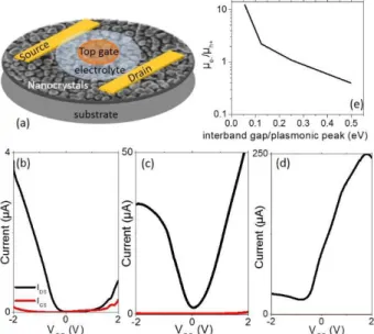
To better highlight the role of doping on the optical properties, we integrate the film of HgTe CQD into electrolyte-gated transistor (see Figure 3a for a scheme of the device).41 Such gating method
is convenient because it combines low bias operation thanks to the large gate capacitance with air operability. As the nanoparticle size is increased, the material switches from p-type (conduction under hole injection) (Figure 3b) to ambipolar (Figure 3c) and finally to
n-type only (conduction under electron injection) for the largest sizes (Figure 3d). This change of behavior is further quantized by the increase of the ratio of electron mobility over hole mobility while the band gap is reduced, see Figure 3e.
This emergence of n-type conduction is similar to what has been observed for HgS8 and HgSe10 nanocrystals. Due to the
combina-tion of narrow band gap and high work funccombina-tion in HgX CQD, the material can be reduced by the environment.42 This reduction
how-ever occurs for much larger size (ie lower confinement) because of the lower work function of HgTe material compared with HgS and HgSe.40 This is interesting on an applied point of view because it
preserves the gate effect even for large particles, while for other chalcogenides gate control is lost due to their too metallic charac-ter.43 This means that even for the largest particle the number of
carrier per particle remains in the range of what can be tuned by electrolyte gating (0-6 electrons typically). As a result, the long wavelength feature observed in the absorption spectra is probably not fully plasmonic and preserves an intraband character.
Figure 3 (a) Scheme of an electrolyte gated transistor which
chan-nel is made of S2- capped HgTe CQD. Transfer curves (current as
a function of gate bias) for HgTe CQD with an excitonic feature at 4000cm-1 (b), a cut off at 2000cm-1 (c) and a plasmonic feature at
450cm-1 (d). (e) Variation of the ratio of the electron mobility over
the hole mobility as a function of the interband gap.
In summary, we report a new synthetic procedure for HgTe nano-crystal, which allows an unprecedented tuning of nanocrystal sizes from small scale to far beyond the exciton Bohr radius. This leads to the first demonstration of colloidal nanocrystals with optical fea-ture in the THz range. The synthesis is also promising for small size because of the low aggregation and good shape control (ie spherical objects) of the synthetized nanocrystals. Moreover, the synthesis relies on low reactivity precursor of mercury with low cost. The transport properties of the nanocrystals show a change of majority carrier density from p-type for small CQD to n-type for the largest object.
ASSOCIATED CONTENT
Supporting InformationThe Supporting Information is available free of charge on the ACS Publications website.
Additional information includes experimental details on HgTe, HgSe and HgS nanocrystal synthesis, TEM pictures of HgTe CQD shape evolution with time and self-assembly in dimer, reactivity of different HgX precursors, absorption spectra with different stoichi-ometry of HgTe CQD, size distribution, experimental details on electron microscopies, UV-Vis, FTIR and Raman spectroscopies (PDF)
AUTHOR INFORMATION
Corresponding AuthorNotes
The authors declare no competing financial interests.
ACKNOWLEDGMENT
EL acknowledges the financial support of the European Research Council (ERC) starting grant (blackQD – n°756225). We acknowledge the use of clean-room facilities from the “Centrale de Proximité Paris-Centre”. We thank Agence Nationale de la Recher-che for funding through grant Nanodose and H2DH. This work has been supported by the Region Ile-de-France in the framework of DIM Nano-K. This work was supported by French state funds man-aged by the ANR within the Investissements d'Avenir programme under reference ANR-11-IDEX-0004-02, and more specifically within the framework of the Cluster of Excellence MATISSE. This work is also supported by the NextIR grant funded by Nexdot.
REFERENCES
(1) McDonald, S. A.; Konstantatos, G.; Zhang, S.; Cyr, P. W.; Klem, E. J. D.; Levina, L.; Sargent, E. H. Nat Mater 2005,
4 (2), 138.
(2) Pietryga, J. M.; Schaller, R. D.; Werder, D.; Stewart, M. H.; Klimov, V. I.; Hollingsworth, J. A. J. Am. Chem. Soc.
2004, 126 (38), 11752.
(3) Kershaw, S. V.; Susha, A. S.; Rogach, A. L. Chem. Soc.
Rev. 2013, 42 (7), 3033.
(4) Low, T.; Avouris, P. ACS Nano 2014, 8 (2), 1086. (5) Withayachumnankul, W.; Shah, C. M.; Fumeaux, C.;
Kal-tenecker, K.; Walther, M.; Fischer, B. M.; Abbott, D.; Bhaskaran, M.; Sriram, S. Advanced Optical Materials
2013, 1 (6), 443.
(6) Isaac, T. H.; Barnes, W. L.; Hendry, E. Appl. Phys. Lett.
2008, 93 (24), 241115.
(7) Pietro, P. D.; Ortolani, M.; Limaj, O.; Gaspare, A. D.; Gil-iberti, V.; Giorgianni, F.; Brahlek, M.; Bansal, N.; Koirala, N.; Oh, S.; Calvani, P.; Lupi, S. Nat Nano 2013, 8 (8), 556. (8) Shen, G.; Guyot-Sionnest, P. J. Phys. Chem. C 2016, 120
(21), 11744.
(9) Yoon, B.; Jeong, J.; Jeong, K. S. J. Phys. Chem. C 2016,
120 (38), 22062.
(10) Lhuillier, E.; Scarafagio, M.; Hease, P.; Nadal, B.; Aubin, H.; Xu, X. Z.; Lequeux, N.; Patriarche, G.; Ithurria, S.; Dubertret, B. Nano Lett. 2016, 16 (2), 1282.
(11) Deng, Z.; Jeong, K. S.; Guyot-Sionnest, P. ACS Nano
2014, 8 (11), 11707.
(12) Jeong, J.; Yoon, B.; Kwon, Y.-W.; Choi, D.; Jeong, K. S.
Nano Lett. 2017, 17 (2), 1187.
(13) Kovalenko, M. V.; Kaufmann, E.; Pachinger, D.; Roither, J.; Huber, M.; Stangl, J.; Hesser, G.; Schäffler, F.; Heiss, W. J. Am. Chem. Soc. 2006, 128 (11), 3516.
(14) Keuleyan, S.; Lhuillier, E.; Brajuskovic, V.; Guyot-Si-onnest, P. Nat Photon 2011, 5 (8), 489.
(15) Lhuillier, E.; Keuleyan, S.; Rekemeyer, P.; Guyot-Si-onnest, P. Journal of Applied Physics 2011, 110 (3), 033110.
(16) Guyot-Sionnest, P.; Roberts, J. A. Appl. Phys. Lett. 2015,
107 (25), 253104.
(17) Chen, M.; Lu, H.; Abdelazim, N. M.; Zhu, Y.; Wang, Z.; Ren, W.; Kershaw, S. V.; Rogach, A. L.; Zhao, N. ACS
Nano 2017, 11 (6), 5614.
(18) Yifat, Y.; Ackerman, M.; Guyot-Sionnest, P. Appl. Phys.
Lett. 2017, 110 (4), 041106.
(19) Tang, X.; Wu, G. fu; Lai, K. W. C. J. Mater. Chem. C
2017, 5 (2), 362.
(20) Chen, M.; Shao, L.; Kershaw, S. V.; Yu, H.; Wang, J.; Rogach, A. L.; Zhao, N. ACS Nano 2014, 8 (8), 8208. (21) Lhuillier, E.; Robin, A.; Ithurria, S.; Aubin, H.; Dubertret,
B. Nano Lett. 2014, 14 (5), 2715.
(22) Tang, X.; Tang, X.; Lai, K. W. C. ACS Photonics 2016, 3 (12), 2396.
(23) Tang, X.; Wu, G. F.; Lai, K. W. C. Appl. Phys. Lett. 2017,
110 (24), 241104.
(24) Nengjie, H.; Shuchi, G.; Gerasimos, K. Advanced
Materi-als 2017, 29 (17), 1606576.
(25) Lhuillier, E.; Guyot-Sionnest, P. IEEE Journal of Selected
Topics in Quantum Electronics 2017, 23 (5), 1.
(26) Keuleyan, S.; Lhuillier, E.; Guyot-Sionnest, P. J. Am.
Chem. Soc. 2011, 133 (41), 16422.
(27) Keuleyan, S. E.; Guyot-Sionnest, P.; Delerue, C.; Allan, G. ACS Nano 2014, 8 (8), 8676.
(28) Sagar, L. K.; Walravens, W.; Maes, J.; Geiregat, P.; Hens, Z. J. Phys. Chem. C 2017, 121 (25), 13816.
(29) Izquierdo, E.; Robin, A.; Keuleyan, S.; Lequeux, N.; Lhuillier, E.; Ithurria, S. J. Am. Chem. Soc. 2016, 138 (33), 10496.
(30) Shen, G.; Chen, M.; Guyot-Sionnest, P. J. Phys. Chem.
Lett. 2017, 2224.
(31) Rinnerbauer, V.; Hingerl, K.; Kovalenko, M.; Heiss, W.
Appl. Phys. Lett. 2006, 89 (19), 193114.
(32) Lhuillier, E.; Keuleyan, S.; Guyot-Sionnest, P.
Nanotech-nology 2012, 23 (17), 175705.
(33) König, M.; Wiedmann, S.; Brüne, C.; Roth, A.; Buhmann, H.; Molenkamp, L. W.; Qi, X.-L.; Zhang, S.-C. Science
2007, 318 (5851), 766.
(34) Malkova, N.; Bryant, G. W. Phys. Rev. B 2010, 82 (15), 155314.
(35) Rowe, D. J.; Jeong, J. S.; Mkhoyan, K. A.; Kortshagen, U. R. Nano Lett. 2013, 13 (3), 1317.
(36) Gordon, T. R.; Paik, T.; Klein, D. R.; Naik, G. V.; Ca-glayan, H.; Boltasseva, A.; Murray, C. B. Nano Lett. 2013,
13 (6), 2857.
(37) Buonsanti, R.; Llordes, A.; Aloni, S.; Helms, B. A.; Milli-ron, D. J. Nano Lett. 2011, 11 (11), 4706.
(38) Delerue, C. Nano Lett. 2017, 17 (12), 7599.
(39) Pearson, R. G. J. Am. Chem. Soc. 1963, 85 (22), 3533. (40) Chen, M.; Guyot-Sionnest, P. ACS Nano 2017, 11 (4),
4165.
(41) Lhuillier, E.; Ithurria, S.; Descamps-Mandine, A.; Douil-lard, T.; Castaing, R.; Xu, X. Z.; Taberna, P.-L.; Simon, P.; Aubin, H.; Dubertret, B. J. Phys. Chem. C 2015, 119 (38), 21795.
(42) Robin, A.; Livache, C.; Ithurria, S.; Lacaze, E.; Dubertret, B.; Lhuillier, E. ACS Appl. Mater. Interfaces 2016, 8 (40), 27122.
(43) Martinez, B.; Livache, C.; Notemgnou Mouafo, L. D.; Goubet, N.; Keuleyan, S.; Cruguel, H.; Ithurria, S.; Aubin, H.; Ouerghi, A.; Doudin, B.; Lacaze, E.; Dubertret, B.; Silly, M. G.; Lobo, R. P. S. M.; Dayen, J.-F.; Lhuillier, E.