A Constraint-based Systems Approach to Line Yield Improvement in Semiconductor Wafer Fabrication
by
Viju S. Menon
M.S.E., Computer Science Engineering University of Michigan, Ann Arbor, 1990
Submitted to the Department of Electrical Engineering & Computer Science and the Sloan School of Management
in Partial Fulfillment of the requirements for the degrees of Master of Science in Electrical Engineering and Computer Science
and
Master of Science in Management at the
Massachusetts Institute of Technology
May 1994
© 1994 Massachusetts Institute of Technology, All rights reserved /.)
Signature of iWuthor -' A Certified by
"4-Department of Electripal Engineering & Computer Science /' MIT Sloan School of Management
May 1994
Associate Professor Charles H. Fine, Thesis Advisor MIT Sloan School of Management
Certified by
Professor Lionel C. Kimerling, Thesis Advisor Department of Material Science Engineering Accepted by
Jeffrey A. Barks, Associate Dean Sloan Master's and Bachelor's Programs
r\
n
r
i . .Accepted by
Y
5
R e eiN
tR.
Morgenthaler,
Chairman
_A Constraint-based Systems Approach to Line Yield Improvement in
Semiconductor Wafer Fabrication
by Viju S. Menon
Submitted to
the MIT Sloan School of Management and
the Department of Electrical Engineering & Computer Science in Partial Fulfillment of the Requirements for the Degrees of
Master of Science in Management
and
Master of Science in Electrical Engineering & Computer Science
ABSTRACT
Intel Corporation is a leading semiconductor manufacturer, with 1993 sales exceeding $8 billion. Since market demand is not the constraint for Intel, the key to maximizing profits lies in maximizing die shipments by improving capacity, die yield and line yield. This thesis adopts a "systems thinking" approach, in confluence with Eli Goldratt's "theory of constraints", to develop line yield improvement tools for semiconductor fabrication.
[ntel's historical approach of responding reactively to major wafer loss events provides very little power to alter the course of those events. This thesis uses Systems Thinking to emphasize the underlying structure driving line yield behavior rather than focusing on discrete wafer loss events, thus uncovering high leverage strategies to improve line yield. Intel has typically prioritized line yield problems and improvement projects based on the number of wafers being scrapped due to each problem. This assumes that the significance of a line yield problem depends only on the number of wafers lost, not on the extent of processing done to the wafers before they were lost. My thesis uses Theory of Constraints to prove that the importance of a line yield loss incident should depend not only on the number of wafers lost, but also on where in the process flow, the loss occurred. This research develops a constraint-based wafer scrap value model to systematically assign relative values to wafers depending on where in the process flow the loss occurred. This approach helps to focus a factory's limited line yield improvement resources on those line yield problems having the most revenue impact.
After identifying fundamental issues that contribute to (or limit) line yield performance, this thesis recommends key changes to management systems, structure, policies, and processes, to attain higher line yields in semiconductor wafer fabrication.
'hesis Advisors
Dr. Charles H. Fine, Associate Professor, MIT Sloan School of Management ]Dr. Lionel C. Kimerling, Professor, Material Science Engineering Department
The author gratefilly acknowledges the support and resources made available to him through the MIT Leaders for Manufacturing Program, a partnership between
Acknowledgments
This thesis was far from an individual effort. Without the assistance of numerous people at Intel, MIT professors, students, and professionals in the field, the data and analysis would have suffered. It would be impossible to list everyone who influenced my thinking, both before and during the thesis, but I would like to thank the most significant contributors.
I am deeply grateful to my company supervisor, Al Stone, for his valuable guidance, support, and timely feedback before, during, and after my internship. Al regularly provided direction for focusing my efforts on solving a problem which was at the same time manageable and beneficial to Intel.
Special thanks go to David Marsing and Dan Goranson for initiating and supporting this internship. Many thanks go to Bob Baker and the entire Fab 9 organization, especially the Factory Support Team for their support and hospitality.
I am thankful to my Steering Committee members Brian Harrison, Brian Krzanich, Bruce Sohn, Don Myers, Jerry Marcyk and Tim Hendry for providing valuable insights and cross-factory support. Special thanks goes to Jacques Vuye and Mike Stark for giving me the opportunity to co-chair and drive the cross-site line yield benchmarking team. I would like to thank all the team members for their valuable help in data collection.
I am deeply thankful to the Intel Manufacturing Excellence Conference organizers for giving me the opportunity to present my findings and recommendations at the January '94 conference. In this context, I also gratefully acknowledge the excellent feedback I received from the conference's four hundred attendees.
I would also like to thank my thesis advisors, Professor Charlie Fine and Professor Lionel Kimerlirlg, for providing me with very valuable support and guidance.
Finally, and most importantly, I thank my parents, and dedicate this thesis to my mother and to the inspiring memory of my father. All of my successes and achievements are a direct reflection of their support, guidance and confidence.
Bibliographical Note on Author
Viju S. Menon graduated from the University of Michigan, Ann Arbor, MI, in December 1990 with a Master of Science degree in Computer Science Engineering. He graduated from the University of Kerala, India, in 1988 with a Bachelor of Technology degree in Computer Science Engineering.
Viju joined Intel Corporation in January 1991 and has worked in various design engineering roles for Intel in Arizona and Oregon. Upon his acceptance to MITs Leaders for Manufacturing program, Intel Corporation decided to sponsor him, and he will be joining Intel's Component's Manufacturing Division (Fab 11, New Mexico) in June 1994. He is currently working towards masters degrees in management and electrical
Table of Contents
1.0 Theme Selection ... ... 15
1.1. Introduction ... 15
1.2 Project Motivation & Problem Definition ... 15
1.3 Project Objectives & Deliverables ... 17
2.0 Data Collection ... ... 18
2.1 Introduction ... 18
2.2 Intel's Technology & Manufacturing Group ... 18
2.3 An Overview of Microelectronic Fabrication ... 20
2.4 Systems Thinking as a Data Collection Framework ... 25
2.5 Line Yield Methodology Data Collection Questionnaire ... 27
2.6 Inter-Fab Line Yield Benchmarking Framework ... 34
3.0 Causal Analysis ... 38
3.1 Introduction ... 38
3.2 Fishbone Diagram Analysis of line yield losses ... 39
3.3 System Dynamics Analysis of line yield losses ... 39
3.4 Summary...6... 61
4.0 Solution Planning & Implementation ... 63
4.1 Introduction ... 63
4.2 What is "Theory of Constraints"? ... 64
4.3 Applying Theory of Constraints to Line Yield ... 67
4.4 A Line Yield Management Tool kit ... 76
5.0 Evaluation ofEffects ... 94
5.1 Introduction ... 94
5.2 Tangible Results of this Research ... 94
5.3 Intangible Results of this Research ... 96
6.0 Standardization ... ... 98
6.1 Introduction ... 98
6.2 The Line Yield Steering Committee ... 98
6.3 The Line Yield Benchmarking Team ... 98
6.4 Intel Manufacturing Excellence Conference '94 ... 99
6.5 Line Yield Road show .... ... 99
6.6 Next Steps ... 100
7.0 Summary of Key Recommendations ... 101
List of Figures
Technology & Manufacturing Group Organizational Structure... General Fabrication Sequence for Integrated Circuits...
Events, Patterns, and Structure in Systems Thinking...
A Systems Framework for Data Collection...
A Systems Perspective to Line Yield Data Collection...
Fishbone diagram of Major causes of Line Yield Losses... Causal Loop diagram of Expected Behavior of EDO Policy...
A Typical Factory Equivalent Die Out (EDO) Pareto...
Demand Curve over Time for x86 Microprocessors ...
Sales Price Curve over time for x86 Microprocessors... Causal loop diagram of actual LY Behavior due to EDO Policy... Causal loop diagram of reasons for slow LY Improvement Rate.... A Pipe of Varying Thicknesses to Illustrate Bottlenecks... A Simple Model of Fab Processing Steps... Increasing Wafer Value due to more processing at Constraints... Wafer Value at each Diffusion Step...
Fab 9 Q3 '93 Diffusion Scrap Wafer Value (disguised numbers)....
Fab 9 Q3 '93 Diffusion Scrap Revenue Loss Pareto (disguised)...
Increasing Wafer Value at Each Constraint Step...
Figure 2.1 Figure 2.2 Figure 2.3 Figure 2.4 Figure 2.5 Figure 3.1 Figure 3.2 Figure 3.3 Figure 3.4 Figure 3.5 Figure 3.6 Figure 3.7 Figure 4.1 Figure 4.2 Figure 4.3 Figure 4.4 Figure 4.5 Figure 4.6 Figure 4.7 19 21 25 26 26 38 40 42 42 42 44 46 65 69 71 74 75 75 81
List of Tables
Table 2.1 Inter-Fab Comparison of Line Yield Definitions ... 34
Table 2.2 Inter-Fab Comparison of Line Yield loss follow-up mechanisms... 36
Table 2.3 Inter-Fab Comparison of Line Yield Communication Strategy ... 37
Table 4.1 Constraint-based model to assess revenue impact of wafer losses.. 73
Table 4.2 Tasks to be done and the right players to improve line yield ... 79
Table 4.3 Constraint-based scrap targets for a simple process flow ... 82
Table 4.4 Methodology for calculating weekly scrap targets for P6x... 83
Reader's Guide
One of the issues I faced at the end of my internship was how to document my research. Since I had used the Seven Step Method for a systematic diagnosis of the fundamental causes of line yield problems, I decided to use the "QI (Quality Improvement) Story" format, which is an efficient sequential format used by seven-step researchers to present to management, the findings of quality improvement studies.
IThe Seven Step Method is a step by step process to systematicallv solve problems.
Chapter 1 (Theme Selection) discusses the line yield improvement theme, and the motivation for this project. It also clearly defines the research objectives and deliverables. Chapter 2 (Data Collection & Analysis) discusses the framework I used to collect and analyze line yield related data at each Intel site.
Chapter 3 (Causal Analysis) introduces the tool (i.e., Systems Thinking) I used to analyze the root causes of line yield problems, and also discusses how I applied systems thinking to uncover underlying causes of slow line yield learning rates at Intel factories. Chapter 4 (Solution Planning & Implementation) first talks about the solution planning tools I used (e.g., Theory of Constraints (TOC), Systems Thinking), and then introduces my solutions including the TOC based wafer scrap value model and other facets of my line yield improvement tool-kit.
Chapter 5 (Evaluation of Effects) discusses the tangible results of my research and also the intangible results in terms of satisfaction level of customers with this tool, skill level, and motivation of people involved in implementing my recommendations. This chapter also discusses communication of my key findings across Intel.
Chapter 6 (Standardization) defines how the solution can be permeated in the company. Chapter 7 (Reflection on the process/Next Problem) discusses key recommendations and findings of my research and also outlines tentative research areas based on this thesis.
Step 1: Theme Selection Step 5: Evaluation of Effects Step 2: Data Collection & Analysis Step 6: Standardization
Step 3: Causal Analysis Step 7: Reflection on Process & Step 4: Solution Planning & Implementation Identification of next problem
Chapter 1. Theme Selection
Purpose: The purpose of theme selection is to recognize the importance of the problem
and to define the problem clearly. This chapter discusses the line yield problem, motivation for this research, the research objectives and deliverables.
1.1. Introduction
Intel Corporation is the world's leading microprocessor manufacturing firm. Much of its recent success is based upon its dominance in providing the microprocessors that run IBM compatible personal computers. In 1981, IBM selected the Intel x86 architecture as the microprocessor that would be used in its initial foray into the personal computer market. Successive generations of this architecture (286, 386, 486, and PentiumTM) have each spurred the rapid deployment of new product lines by PC manufacturers.
The ability of Intel, as well as the other semiconductor manufacturers, to ramp new products and processes has become critical in today's business environment [1]. In fact, competition in many industries has moved beyond quality and performance to reaching the target market in the required time window. Intel Corporation has now committed itself to more rapid introductions of new generations of microprocessors. In order to achieve this goal, design teams for different microprocessor generations are now working in parallel on their circuit designs. This approach as well as the use of sophisticated software tools will enable more rapid releases of product designs. The important challenge facing Intel and other semiconductor firms is whether their manufacturing facilities can match the accelerating pace of the designers when they ramp production of new microprocessors.
1.2. Project Motivation & Problem Definition
Factory output is a function of installed equipment base, utilization of that equipment, and yields. Yields include both line yield (the % of wafers that make it through the entire process) and die yield (the % of good die in each wafer). Output is ramped through the simultaneous installation of capacity and improvement in yields. Various studies within Intel have shown that of the three output levers (capacity, line
improvements have higher die output leverage than line yield improvements. This has
led Intel to focus its efforts on learning how to ramp up capacity and die yields, with the
result that it now has a better understanding of driving rapid capacity ramps and die yield
improvements [1].
While Intel has historically made dramatic progress in capacity and die yield improvements, it still has to better understand the complex issue of line yield improvement, in terms of understanding the controllable factors causing line yield losses. This would require reviewing all contributors of line yield losses, including equipment, process, and procedural (human) elements to see if there are intrinsic, systematic causes to line yield losses.
Each of the 5 evils (waste, delay, mistakes, defects, accidents) could describe the problems of having line yield losses. A line yield loss results in wasting human and capital equipment resources that were used in processing the wafer before it was scrapped. Depending on where the loss occurred in the process flow, it may result in delaying shipments to customers. It could be the result of a mistake in terms of misprocessing, it could be the result of defective equipment, or it could be the result of an accident. Each of these evils provided strong motivation for initiating this project. Once the theme of line yield improvement was selected, the next step was to set challenging, but realistic, measurable goals, keeping in perspective the 7 month internship time frame.
Key Project Objectives
To develop and provide line yield management models to enable Intel to attain (a) faster line yield learning rates for new processes
(b) step function improvements in line yield for mature processes
Key Project Deliverables
* Document the line yield methodologies at each Intel wafer fabrication plant. - Collect line yield related data on process, equipment & human elements. * Compare line yield definitions and trends at each Intel wafer fabrication plant. * Analyze the line yield management systems at each Intel wafer fabrication plant.
- Deliver a survey and analysis of the line yield methodology used at each site. - Deliver a Pareto of line yield loss causes at various stages of process maturity. * Develop, refine, and apply conceptual models for line yield improvement.
* Recommend key changes to management systems, structure, policies, and processes, to accomplish world class line yield performance at Intel.
Chapter 2. Data Collection
2.1 Introduction
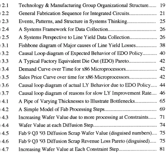
The line yield improvement recommendations and findings discussed in this thesis are based on research performed at Intel's Technology & Manufacturing Group's various technology development and wafer fabrication facilities in New Mexico, Arizona, California, Oregon, and Israel. The nature of this research makes it important to understand the organizational context in which my model was developed and applied. For this reason, this chapter starts with an overview of Intel's Technology & Manufacturing Group. This overview is followed by a discussion of the silicon wafer fabrication process [7,19]. This chapter then discusses the benchmarking [2] framework I used to collect, document, and analyze line yield related data at each Intel site.
2.2 Intel's Technology & Manufacturing Group
At a time when silicon manufacturing is not viewed as strategic by companies that design chips and then have them manufactured outside, Intel's perspective is that manufacturing and process technologies are areas of strategic competitive advantage. According to Intel, having the most advanced process technology is key to being able to design and manufacture leading edge microprocessors. Intel's expertise and continuing investment in process and manufacturing technology indeed help to give it a significant advantage over competitors. Over the years, Intel's manufacturing processes have been refined to allow for chips with smaller circuit sizes, fabricated on larger wafers. The company's first products were made on 2-inch wafers; today, Intel's most advanced products are made on the new 0.6-micron technology process using 8-inch wafers.
Purpose: The purpose of data collection is to investigate the specific features of the
problem from a wide range of different viewpoints. In other words, this phase identifies factors that are the most important things to investigate for root causes in Step 3 (causal analysis). This chapter discusses the framework I used
Senior VP, Technology & Manufacturing Group
ILVCUIU ra 10
Figure 2.1 TMG (Technology & Manufacturing Group)'s Wafer Fabrication
and Process Development Sites & Organizational Structure
The Technology Development (TD) sites at Oregon and California (Figure 2.1) have the charter to develop and deliver new processes that yield at "manufacturable levels". In other words, their charter is to bring the new processes they develop, to a point where the die per wafer yields are high enough to make high volume fabrication economically feasible. Historically, the emphasis has been on developing process technology in a stable environment (e.g., at low volumes). When they got the yields up on a new process, the high volume manufacturing sites (Fabs) had to replicate the process exactly. The Fabs then had to (1) copy exactly, the processes developed in the technology development sites, and (2) ramp the production volumes and yields.
The overriding goal of meeting yield targets in a TD site directly competes with another activity: surfacing potential problems [1]. Surfacing potential manufacturing obstacles requires stressing a system that is closely aligned with the Fab environment. However, this works against getting the process up and running smoothly in the TD site. Moreover, some problems arise only in a full scale manufacturing environment, which differs from development in many areas including personnel policies, equipment capacity and utilization, and operational scale and procedures. These differences result in Fabs and TDs adopting differing line yield management practices, which are discussed in Chapters
3 & 4 of my thesis. My research was based out of Fab 9 in Rio Rancho, New Mexico.
I .. .
2.2.1 Fab 9
Although my research and data collection efforts led to significant travel to several Intel sites, my home base was Intel's highest volume wafer fabrication plant, Fab 9, in Rio Rancho, New Mexico. Fab 9 is currently Intel's largest and most profitable logic factory. Fab 9's charter is to manufacture a variety of microprocessors (primarily the 486 and PentiumrM)processors on micron and sub-micron 6-inch Silicon wafer technologies.
2.3 An Overview of Microelectronic Device Fabrication
Although semiconductor materials have been used in electronics since the early decades of this century, it was the invention of the transistor in 1948 that set the stage for what would become one of the greatest technological advancements in all of history. Semiconductors have become the foundation for electronic devices because their electrical properties can be altered by adding controlled amounts of selected impurity (dopant) atoms into their crystal structures. The electrical operation of semiconductor devices is controlled by creating regions of different doping types and concentrations. Although the earliest electronics devices were fabricated on germanium, silicon has without a doubt become the industry standard.
2.3.1 Crystal Growth and Wafer Preparation
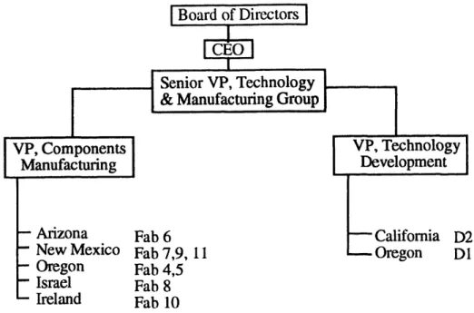
Silicon occurs naturally in the forms of silicon dioxide and various silicates. They must undergo a series of purification steps in order to become the high-quality, defect-free, and single crystal material required for semiconductor device fabrication. Single crystal silicon is almost always obtained by using the Czochralski process [19], utilizing a seed crystal that is dipped into a silicon melt and then slowly pulled out while being rotated. At this point, controlled amounts of impurities can be added to the system to obtain a uniformly doped crystal. The result of this growing technique is a cylindrical single-crystal ingot, typically 50-200 mm (2-8 inches) in diameter and over 1 m in length. Next, the crystal is sliced into individual wafers about 0.5 mm thick. Finally, the wafers must be polished and cleaned to remove surface damage caused by the cutting process. These silicon wafers provide the starting material at Intel. Device fabrication takes place over the entire wafer surface, and hundreds of identical circuits are generated on each wafer at the same time. Once processing is completed, the wafer is sliced into individual
Repeated
Figure 2.2. Generalfabrication sequence for integrated circuits.
Figure 2.2 outlines the processes used in fabricating microelectronic devices and integrated circuits. This section also briefly discusses each of the major fabrication steps
[7,9, 19].
23.2 Film Deposition
Films of many types, particularly insulating and conducting, are used extensively in microelectronic device processing. Examples include polysilicon, silicon nitride, and silicon dioxide. Some of the major functions of deposited film include masking for diffusion or implants, and protection of the silicon surface. In masking applications, the film must effectively inhibit the passage of dopants while also displaying an ability to be etched into patterns of high resolution. Upon completion of device fabrication, films are applied to protect the underlying circuitry. Conductive films are used primarily for device
interconnection. Film deposition techniques involve a variety of temperatures, pressures, and vacuums such as evaporation, sputtering, and chemical vapor deposition (CVD).
23.3 Oxidation
Oxidation refers to the growth of an oxide layer by the reaction of oxygen with the substrate material. Silicon dioxide is the most widely used oxide in IC technology today. Typical functions are dopant masking, device isolation, and surface passivation. Modern IC technologies require oxide thicknesses in the hundreds and thousands of angstroms. Dry and wet oxidation techniques are used for coating the entire silicon surface. Selective oxidation is used to oxidize only certain portions of the substrate.
2.3.4 Lithography
Lithography is the process by which the geometric patterns that define the devices are transferred from a mask to the substrate surface. In current practice, the lithographic (or "litho") process is applied to the wafer surface several times, each time using a different mask to define the different areas of the working devices. Once the film deposition process is completed and the desired masking patterns have been generated, the wafer is cleaned and coated with an emulsion, called photoresist (PR), which is sensitive to ultraviolet light. The wafer is then aligned under the desired mask in a mask aligner. This crucial step is called "registration". Once the wafer and mask are aligned, they are subjected to UV radiation. Upon development and removal of the exposed PR, a duplicate mask pattern will appear in the PR layer.
One of the major issues in lithography is line width, which refers to the width of the smallest feature obtainable on the silicon surface. As circuit densities have escalated over the years, device sizes and features have become smaller and smaller. Today, minimum commercially feasible line widths are 0.8 to 0.6 microns.
2.3.5. Etching
Etching is the process by which entire films or particular sections of films are removed, and it plays an important role in the fabrication sequence. An important criterion in selecting an etchant is its selectivity, which refers to its ability to etch one material without etching another. An etching process must effectively etch the silicon
dioxide layer with minimal removal of the underlying silicon or the resist material. In addition, polysilicon and metals must be etched into high resolution line with vertical wall profiles and minimal removal of the underlying insulating film.
23.6 Diffusion and Ion Implantation
The electrical operation of microelectronic devices depends on regions of different doping types and concentrations. The electrical characteristics of these regions is altered by introducing dopants into the substrate by the diffusion or ion implantation processes. This step in the fabrication sequence is repeated several times, since many different
regions of microelectronic devices must be defined.
In the diffusion process, the movement of atoms results from thermal excitation. Dopants can be introduced to the substrate surface in the form of a deposited film, or the substrate can be placed in a vapor containing the dopant source. The process takes place at elevated temperatures, usually 800-1200 degree centigrade. Dopant movement within the substrate is strictly a function of temperature, time, and the diffusion coefficient of the dopant species, as well as the type and quality of the substrate material.
Ion implantation is a much more extensive process and requires specialized equipment. Implantation is achieved by accelerating ions through a high voltage field of as much as one million electron-volts and then choosing the desired dopant by means of a mass separator. The major advantages of ion implantation including a high degree of anisotropy and wider range of dopant species has made it the dominant technique in modem IC technology.
23.7 Metallization and Testing
Generating a complete and functional integrated circuit requires the individual devices fabricated on the wafer surface, to be interconnected. Interconnections are made by metals that exhibit low electrical resistance and good adhesion to dielectric insulator surfaces. Aluminum, aluminum-silicon-copper alloys, and tungsten are the materials commonly used for this purpose in VLSI technology today. The metal is deposited by standard deposition techniques, and interconnection patterns are generated by lithographic and etching processes. Modern ICs can typically have 1-4 layers of
metal are connected together by vias and access to the devices on the substrate is achieved through contacts.
Wafer fabrication is complete upon application of a passivation layer, and the next step is to test each of the individual circuits on the wafer. Each chip (or die) is tested with a computer controlled probe platform that contains needle-like probes to access the aluminum pads on the die. The platform steps across the wafer, testing whether each circuit functions properly with computer generated simulations. If a defective chip is encountered, it is marked with a drop of ink. After completion of this primary testing, each die is separated from the wafer using diamond sawing. The chips are then sorted.
2.3.8 Bonding, Packaging, and Final Testing
The working dies must be attached to a more rugged foundation to ensure reliability, and they must be accessible to electrical connections to the outside world. Bonding pads are located around the perimeter of the die. The most popular method of attaching these pads is by "wire bonding", which utilizes very thin gold or aluminum wire. The pads are
attached by thermocompression, ultrasonic, or thermosonic techniques.
The connected circuit is now ready for final packaging. Packages are available in a variety of styles. Consideration of a circuit's package includes chip size, number of external leads, operating environment, heat dissipation, and power requirements.
After the chip has been sealed in the package, it undergoes final testing. Because one of the main purposes of packaging is isolation from the environment, testing at this stage usually encompasses heat, humidity, mechanical shock, corrosion, and vibration. Destructive tests are also performed to investigate the effectiveness of sealing.
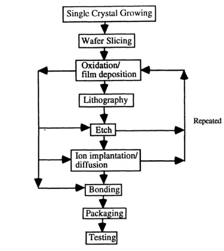
2.4 "Systems thinking" as a framework for data collection
Data collection can be approached from various perspectives as shown in Figure 2.3.
n What happened ?
/ Trends \ What has been happening ? (Forces at Play)
Figure 2.3. Events, Patterns, Structure
Event level: Data collection at this level helps answer the questions: "What happened?
What crisis are we facing?". An example would be line yield loss events. Much of the attention is on daily events, responding and reacting to something that has happened. This level of data collection and action provides very little power to alter the course of these events. The best hope is for an optimal reaction.
Trend or pattern level: Data collection at this level answers the questions: "What has
been happening ?". An example would be a deteriorating line yield trend in a Fab. This mode helps us to take a step back and look at trends, hoping to understand why a recent event has happened based on a number of events in the past. This level of data collection provides us very little power to alter the course of patterns and trends. The best hope is
that the trends continue and the manager optimally responds to them.
Structural level: Data collection at this level leads us to answer the questions: "Why has
it been happening?". An example would be policies affecting line yield improvement. By considering the relationships that exist among the components of the entire organization, this level of data collection fosters a more holistic approach to developing coherent solutions. Structural explanations address the underlying causes of behavior at a level that patterns of behavior can be changed. Structure produces behavior, and changing
underlying structures can produce different patterns of behavior [16].
In this thesis, I have taken a systems thinking approach to data collection and analysis, which has revealed that underlying structure [16] does drive line yield behavior, and that
maximum leverage comes from changes at the structural level. Aspects of structural level
data collection are illustrated in Figure 2.4.
Emotions /ierarchy Physical
Structure
\
Hot ButtonsHabits & Norms aterial Flows Control
Reward Systems Mechanisms
Figure 2.4. A Systems Framework for Data Collection
Applying this structural level approach to collecting data specifically for line yield improvement revealed several underlying structural facets driving line yield behavior. The major structural forces shaping line yield behavior are shown in Figure 2.5. The associated causal loop diagrams are shown and discussed in chapter 3.
Factory Priority
Reward Systems
Resource Allocation for line yield
Line yield loss follow-up systems
Reactive Excursion Fire-fighting
Root cause analysis techniques
for Iline yield
Baseline Training
Line Yield Ownership
Equipment Reliability Factory Floor Involvement
Process maturity at TD Transfer
Figure 2.5. A Systems Perspective to Line yield data collection
lss event
s
sorcal line yield trends
A number of approaches were used to arrive at the list of structural forces described above: face-to-face interviews (both structured and unstructured), remote conversations (via telephone and e-mail), attendance of meetings, site visits, and plant tours. I conducted interviews on a 1-1 basis, and interviewed plant managers, manufacturing and engineering managers, team-leaders, engineers, shift managers, shift supervisors, operators, and technicians on the factory floor. I attended numerous meetings that enabled me to understand several operating policies in the factories. I also co-chaired a ten member inter-site line yield benchmarking team.
2.5 Line Yield Methodology Data Collection Questionnaire
Based on the above knowledge sources, I designed a line yield methodology questionnaire, which I then used to collect data and document the line yield improvement
methodology of each Intel Fab and TD site. One of my deliverables for Intel was a comparison of its factories along several dimensions related to line yield. Since the data
is proprietary to Intel, it is not included in this thesis document. However, the
questionnaire, and the format I used for comparing the various factories is described in this chapter. Both the questionnaire and the comparison format can be adopted by any semiconductor manufacturing firm, to analyze the line yield methodologies followed in their factories. The questionnaire and the comparison format are as follows:
Line Yield Methodology
Questionnaire
Viju Menon
General Fab Information
Name: Location:
Age of Fab: Process(s):
Process Maturity & LY Historical Trendsfor each process
process name:
Startup date:
Please provide the following graphs
Wafer Starts Per Week (WSPW) versus Time graph: Line Yield versus Time graph:
Line Yield Loss cause Pareto from startup by quarter - by process, people, equipment
a) For the whole factory b) For each functional area
- Lithography - Etch
- Thin Films - Diffusion/Implant Die Yield (ISO) versus Time graph
1. Please comment on the above Paretos to explain excursions/abnormal behavior, if any. 2. Please describe in a paragraph how the loss cause paretos have changed since ramping
up from a minimum volume threshold (say 1000wspw). Both, the loss cause contribution by a) process, people & equipment and b) by cluster. What improvements led to these changes in the paretos historically.
3. Please list historical key losses in LY, what methods were adopted to deal with these, and the success of these methods, so as to provide leamings to other factories.
Existing Line Yield Analysis System
a. Definitions
1. How is Line Yield defined and calculated? (please provide equations).
What are the factory floor line yield metrics? e.g. %LY, Losses per 10,000 activities? 2. Do line yield calculations include
a. monitor, short loop and engineering losses? b. sort zero yield wafers ? low yielding wafers? c. ETEST losses?
d. losses due to natural disasters (e.g. power loss)?
e. miscellaneous/other?
3. Do die yield calculations include a. all wafers that make it to sort? b. only the wafers that are shipped out?
c. miscellaneous/other?
4. Where are the sort limits set? How are these established?
b. Data collection, tracking, and analysis
1. What is the database system used to track wafer losses? (e.g. LCS)
2. Please describe the documentation process while scrapping wafers. Does it depend on number of wafers scrapped? Who receives this documentation? Please include samples of document(s) generated when a wafer is scrapped.
c. Disposition methods (to et a flavor of the operating philosophy)
1. Who is allowed to scrap material in-line? Who actually does the scrap? Technicians, Operators or Engineers? (To get a flavor of whether it is more objective or judgemental) Are spec limits for scrap well defined?
2. Are spec limits for scrap well defined? Are spec limits established using statistical bin limits, or are they true spec limits?
3. Do you use statistics in setting disposition limits in the fab, etest, and sort areas? Are
wafers out of SPC control always scrapped?
3. If a wafer fails spec, is it always scrapped? Do you challenge specs with each scrap? If not, how often is it done?
4. Are wafers out of spec passed and out into quarantine? How many wafers are currently (or typically) in quarantine?
5. Do you tend to pass wafers on and screen them at e_test & sort?
6. When production wafers get scrapped, do they get downgraded to engineering wafers?
If so, how does line yield get affected? Is this a line yield loss?
7. Do you have a procedure for bonusing or upgrading wafers back into production?
c. Follow-up or Postmortem System for the documented losses
1. Who tracks the documented losses (e.g. first order scrap reports)?
2. What is the forum where the documented losses get addressed? Who owns this postmortem co-ordination? What are the roles & responsibilities of the members of this forum? How often are they conducted?
3. Who presents at the postmortem about the losses? How do the presenters view the forum? (intimidatory ?) Typical Agenda? Do they discuss both line yield & die yield in this forum?
5. What is the follow-up system for action items generated at the postmortem? Please include a flowchart of the documentation, postmortem, and follow-up processes'? 6. Do the people doing the scrap documentation get feedback on the analysis of the scrap
&. root cause fixes? Is there a feedback loop?
7. What in the system ensures a closed loop, between generating documents for losses, and implementing fixes for the losses documented?
e. Root Cause Analysis
1. What are the conditions under which root cause analysis is done for scrap?
2. What is used to prioritize what line yield problems are worked on? How do you distinguish between an excursion mode issue and a baseline issue? How do resourcing and root cause analysis systems work for excursion and baseline issues?
3. What is the forum at which root cause analysis gets done?
4. Is there a documented structured procedure for root cause analysis ? How do you establish causality ? Is it empirical evidence, statistics, FMEA, seven step method, or is the root cause analysis an adhoc procedure?
5. Do e_test & sort losses get billed back to the appropriate clusters ? How is it done ? Who does the causal analysis for e_test & sort losses?
6. Please describe a typical real life scrap incident and provide a walk through of how the system operates (from the scrap decision, documentation, through root cause analysis and fix implementation)?
f.
Implementing Root Cause Fixes1. What is the forum where implementing root cause fixes gets addressed?
2. What is used to prioritize what line yield fixes are implemented?
3. Please address ownership, responsibility & accountability for the question below.
What actions are taken when the fix is identified to be
a) process related b) equipment related c) procedural related
4. Please give specific examples for each of the above in a paragraph each.
g. Line Yield Improvement Efforts
1. How would you define roles and responsibilities of each of the functional departments in line yield improvement?
2. What reactive & proactive measures are taken by these departments? 3. Is each of these departments in a reactive or pro-active mode of operation?
4. Are there formal line yield improvement programs? Is there a dedicated individual/group that owns driving line yield improvements?
Departments: Manufacturing Process/Eqpt Eng: Factory Support Industrial Engineering Training
Functional Area Teams
Yield Engineering Automation Other 5. Please comment on any suggestions you may have on improving line yield?
h. Line Yield related Success Indicators
i. Communication Strategy for Line Yield
I: --r I
1. Is overall line yield well known on the factory floor?
2. Does each equipment cluster know what their contribution to line yield loss is?
3. What is the communication mechanism for people on the factory floor? Is it part of the normal visual experience e.g. ( display boards, shift passdowns) or is it just on the computer (e.g., vax, bulletin boards) that people have to look up?
4. Does each cluster have a line yield goal? Do the people know what their goal is? 5. Who establishes line yield goals for each cluster? Who drives this goal?
6. Do the factory personnel generating scrap reports feel comfortable about entering the correct loss cause? Has the message been conveyed to them that they wont get
disciplined, and that the report will be used for identifying the correct root causes? 7. Are there any incentives for people to be frank & enter the correct loss code?
Miscellaneous
1. What systems are in place for fabs to learn from each other to avoid problems faced and solved by the other fabs?
For each of the departments listed above,
1. Is Line Yield a CSI (Critical Success Indicator) for that department? 2. If it is a CSI, How is it communicated ? (e.g., dept meetings, passdown)? 3. In what forums does line yield get talked about in each department? 4. What are the top three priorities for each department?
5. What is the budget ($) for line yield improvement? What are the quarterly goals? 6. What are the positive incentives (reward systems) for line yield performance?
7. What if any are the negative incentives (disciplinary systems) for not meeting line yield goals?
2.6 Inter-Fab Line Yield Benchmarking Framework
Once the answers to the questionnaire were documented for every Fab, the next step was to compare the line yield methodologies adopted in the various factories, and to document the comparison framework in a concise format. The format I used to compare various aspects of line yield, such as definitions, management methods, feedback systems, communication strategies, etc. are outlined below:
2.6.1. Inter-Fab Comparison of Line yield definitions:
A fundamental issue in benchmarking is to make sure we are "comparing apples to apples". Thus, when comparing line yield performances of various factories, it was crucial to ensure that each Fab was calculating line yield in the same way.
Table 2.1. Inter-Fab Comparison of Line Yield Definitions:
Factory Line Yield Fab A Fab B Fab C Fab D Fab E Fab F Fab G Fab H Fab I calculation includes Monitor wafers Shortloop wafers , Engineering
wafers
__,_ Production wafers Electrical-test wafers Sort low yield wafersSort Zero yield wafers
Wafer losses due to facilities losses Wafer losses due to Natural disasters
When presented with a trend graph showing the line yield % achieved at several factories over a period of time, it is important to consider how each factory arrived at their line yield numbers. The first column in Table 2.1 shows the various types of wafers that may or may not get included in each Fab's line yield calculations. Each entry in Table 2.1 can contain either a 'Yes' or 'No', indicating what kinds of wafers are included in line yield calculations at each factory. The specific answers from each site are not included due to confidentiality reasons. However, this format would be useful to compare line yield
performances in any bench marking effort, either within another company, or among other companies.
2.6.2. Inter-Fab Comparison of Line Yield Loss Follow-up Methodologies:
Line yield management methodologies varied on several aspects across the various Fabs. A critical component of any line yield methodology is the mechanism used to keep track of wafer losses, following up on analyzing causes of major losses, and implementing root cause fixes. In other words, ensuring a closed loop follow-up system where root cause fixes will get implemented at least for major problems selected for investigation. Table 2.2 represents the format I used for comparing the follow-up systems at the various Fabs.
2.6.3. Inter-Fab Comparison of Line Yield Communication strategy & incentives:
Another critical component of any line yield methodology is the communication strategy and incentive structure used to increase awareness, involvement, ownership, and accountability of factory floor personnel in line yield improvement. Table 2.3 represents the format used to compare such facets of line yield methodologies at the various Fabs.
Table 2.2. Inter-Fab Comparison of Line Yield Loss Follow-up Mechanisms:
LY Loss tracking & Fab A Fab B Fab C Fab D Fab E Fab F Fab G Fab H Fab I Follow-up systems
What Databases are
used to track losses? .
Who receives the loss notification? Wafer loss threshold over which losses are documented? Who is responsible for tracking these documents?
What are the forums where these losses are addressed? Are Postmortems conducted for losses? Who coordinates the
Postmortems? _
Who attends the Postmortems? How frequently are Postmortems held? Who presents losses at the Postmortems? Loss threshold above which Postmortems are conducted? Who follows up on tasks assigned at Postmortems? Is the Follow-up loop
Table 2.3. Inter-Fab Comparison of
Line Yield Communication Strategy & Incentive Structure:
Facets of Strategy Fab A Fab B Fab C Fab D Fab E Fab F Fab G Fab H Fab I Is line yield well
known on the Floor? Does each cluster know their
contribution to LY? What is the mode of communicating LY to the Factory floor? Does each equipment cluster have a line
yield goal? Do people in each cluster know their line yield goal? What is the metric for measuring LY? (%LY, Loss/lOK)? Who drives cluster line yield goals? Are there any positive line yield rewards? _
Are there negative incentives for poor LY performance? Are there any formal LY programs?
Chapter 3. Causal Analysis
Purpose: The purpose of causal analysis is to find out what the main causes of the
problem are. This chapter identifies fundamental issues that contribute to (or limit) Intel's line yield performance.
3.1 Introduction
This chapter analyzes the data collected via the line yield questionnaire, and arrives at root causes of line yield losses that cause slow line yield learning rates. The two tools I used were Ishikawa (Fishbone) diagrams and Systems Thinking[16]. I used Ishikawa diagrams to arrive at the first order causes. Then, I used causal loop diagrams and systems thinking principles to arrive at the fundamental issues underlying line yield losses.
3.2 Fishbone Diagram Analysis of line yield loss causes
Figure 3.1 shows my first order Fishbone diagram analysis of the major factors causing line yield losses. As this diagram indicates, line yield is indeed a very complex issue with multiple interactions among loss causes. This Fishbone diagram does not provide, and is not intended to provide, a comprehensive representation of all the underlying causes of line yield losses. Instead, it is intended to give the reader a flavor of the major line yield loss causes, the complexity of the problem, and to set the stage for the in-depth discussion
following in the next section.
3.3. Systems Thinking analysis of line yield loss causes
All line yield losses are typically attributed to one of three major causes (a) equipment malfunction (b) process marginality (c) misprocessing, or in other words, human error. However, when we dig deeper, we find that these categories are not really causes in themselves, but are only symptoms of underlying problems. For instance, consider a line yield loss incident caused by an operator running the wrong recipe for a process step. Our typical response would be to attribute the loss to irresponsible operator behavior, and to categorize the loss as "human misprocessing". A typical remedial action would be to counsel the operator. However, the fundamental reasons may not lie with the operator at all. Maybe the operator had to juggle various lots of wafers each of which required a different recipe, in which case, it would be very easy to mix up lots and run the wrong recipe. The long term fix maybe lies in installing a station controller at that work-station, not in counseling the operator.
In fact, I would hypothesize that the vast majority of line yield problems are caused by systemic issues that transcend simple explanations such as "equipment failure", "process immaturity", and "human screw up". The following section highlights several underlying reasons for line yield losses and slow line yield improvement rates exhibited at wafer fabrication plants.
How do factories approach line yield improvement ? Has it been a high factory priority ? The aim of a factory is to maximize revenue and profits. At Intel, where market demand is not the constraint, this aim is achieved by maximizing die shipments. The three levers
improving equipment availability and utilization (b) improving die yields (c) improving line yields. The simple causal loop diagram (Figure 3.2) illustrates the expected behavior of this policy. An arrow labeled '+' connecting 2 variables indicates that a change in one direction of the first variable results in a change in the same direction of the other variable. For example, Increasing the EDO goal in the diagram below will increase the EDO Gap. An arrow labeled '-' indicates that the variables change in opposite directions. For example, Increasing 'Current actual Die Output' decreases the 'EDO Gap'.
Press Die Output
1
incre.(EDO)
Goal
"'
EDO Gap
Curre Die C
Figure 3.2. Expected Behavior of EDO Policy
However, since improvement opportunities may exist in all three areas (capacity, line yield, die yield), and since a Fab has only limited resources to work on improvement projects, the plant management prioritizes improvement projects according to their impact on maximizing die output. Typically, every quarter, the senior management in a factory prioritizes potential capacity, die yield, and line yield improvement projects based on quantifiable incremental die output resulting from the completion of each project. EDO is "equivalent die out", defined as the total weekly output of the factory measured by normalizing all good die to the equivalence of a single product. The goal of the factory is to maximize EDO.
EDO = Min (WSi) x DPW x LY x DY
WSi: Output of the ith station in WSPW (Wafer Starts Per Week), Min(WSi) is the output of the bottleneck station which limits the factory. DPW: Number of potential good die per wafer.
LY: Factory Line Yield in % = product of line yields at each station in the process flow. DY: Process (or Product) Die Yield in %.
The inputs to the evaluation process are (a) Line Yield loss Pareto for the previous quarter, which identifies the potential line yield improvement projects. Only quantifiable and realizable line yield projects are chosen for consideration. e.g., projects to increase line yield at a particular functional area such as lithography or diffusion get chosen, while projects to reduce procedural errors across the entire factory do not get chosen, because of its wide scope and difficulty of implementation (b) Die Yield loss Pareto for the previous quarter (c) Capacity limiter Pareto, which identifies the existing potential capacity improvement projects.
The evaluation process is as follows: DPW is held constant throughout the process. For determining the EDO opportunities of each capacity project, the other variables in the EDO equation, LY and DY, are held constant (say, at 100%). Similarly, while calculating the EDO impact of LY projects, DY and Capacity are held constant, and while determining the EDO impact of DY projects, LY and Capacity are held constant.
The output of the evaluation process is a Pareto, ranking each potential improvement project in terms of its EDO impact. This Pareto is called the EDO Pareto. The limited improvement resources available (in terms of human and capital resources) are applied to the biggest Pareto items. Typically this results in several low EDO leverage improvement projects not being addressed due to lack of resources.
As part of my research, I studied the EDO Paretos at several Fabs, at several stages of process and factory maturity. Historically. right from factory sart-up. all the way until after ramp. the EDO Pareto (Figure 3.3) indicates that capacity and die yield improvement projects have higher die output leverage than most line yield improvement Proiects.
EDO Impact
Capacty
ield
Potential Improvement Projects
Figure 3.3 A Typical Factory EDO Pareto
Possible reasons why Line Yield is behind capacity and die yield on the EDO Pareto:
Demand (units per month) Sales Price per unit Time Time Figure 3.4 Figure 3.5
Intel's bread-and-butter lies in its leading edge microprocessors. Figure 3.4 shows a typical x86 microprocessor demand life cycle. Figure 3.5 traces the average sales price of a microprocessor at various stages in its life cycle. Most of the unit revenues generated for a new product occur soon after its introduction while demand for the product is booming. Due to the absence of clones at this stage, Intel can command high prices. Operating margins are highest in that time period. Demand typically outstrips supply at this stage, and there is tremendous pressure to increase factory output since revenue and profits are directly proportional to factory die shipments.
This leads the factory management to search for EDO improvement opportunities that quickly increase EDO with a high level of certainty. Note that "quick returns", "high
I
-probability of success" and "tangible effort requirement", are critical in selecting potential EDO improvement opportunities. These may not correspond to projects that fetch the "most bang for the buck", especially in cases where cost-effective projects do not fetch quick returns, or when cost-effective projects require wide-spread and not focused efforts. This explains the bias towards capacity and die yield improvement
projects, and the bias against line yield improvement projects.
Although adding a new machine to increase die shipments may not be as cost-effective ;as improving yields, the resulting increase in capacity will fetch a faster and greater increment in EDO. Especially for state-of-the-art processes, die yield improvement entails focused engineering efforts, and although such projects have a high probability of success, they are time consuming, and not as easy to achieve as adding another machine. ]However, die yield efforts are still preferred to line yield efforts by factory management because line yield improvement is even more difficult to achieve in a short time frame than die yield. This is due to the fact that line yield is a complex function of procedural (human) errors, operating philosophies, equipment reliability, and process marginality, while die yield is primarily an engineering intensive problem with very little procedural error intricacies.
The bias towards identifying EDO improvement projects that (a) have quick returns (b) require focused effort (c) have high probability of success have a big influence on what kind of line yield projects are even considered to be included on the EDO Pareto. The Factory Wafer Scrap Pareto for the previous quarter (3 months) provides the list of potential line yield projects to be considered as inputs to the EDO evaluation process. At first glance, this appears okay, because it provides a list of the top line yield problems existing in the factory. Only those line yield projects requiring focused effort (mostly excursions), that are perceived as realizable within a relatively short time horizon (1-2 quarters) are considered. This Pareto contains individual station (or functional area) line yield losses, and does not include high leverage (baseline) line yield projects of global scope, such as reduction of procedural errors across the factory floor. For the most part, line yield excursions make it higher in the EDO Pareto than baseline losses that are more spread out across functional areas.
Implications of the EDO "low priority" policy on line yield:
The causal loop shown in Figure 3.2 shows the expected behavior of the EDO policy. However, in reality, there are various interactions that are not reflected in that diagram. The low EDO line yield priority causes various dynamic interactions, some of which are reflected in Figure 3.6. £ Die Output (EDO) Goal Pressure to EDO Gap Current actual Die Output
Figure 3.6. Actual Behavior due to low line yield EDO Prioritization
Due to the lower EDO line yield priority, initially more emphasis is given to improving die yield and capacity. As the above diagram indicates, this emphasis on die yield and capacity negatively impacts line yield performance in several ways. Rapid capacity expansion results in lower stability of operations in the ramp phase, which increases the
occurrence of line yield excursions. High levels of equipment uptime and utilization often leads to iegularities in carrying out preventive maintenance procedures, and increased stress on the machinery, which in turn leads to line yield losses. Emphasis on die yield improvement occupies significant engineering resources, leaving very few resources for baseline line yield improvement. All these reasons induce reactive fire-fighting. Another factor is the long delay involved between initiating baseline efforts and seeing tangible improvement in line yield as a result of these baseline efforts. This delay promotes even more emphasis on quick "band-aid" fixes, promoting excursion fire-fighting.
Since factory priorities are driven by the EDO Pareto, the apparently low line yield leverage influences management's mindset towards line yield improvement in the start-up and ramp stages of' the process, and results in lower factory priority for line yield. Figure 3.7 illustrates the "success to the successful" system dynamics archetype where two activities compete for limited resources. The more successful one becomes, the more support it gains, thereby starving the other. The low priority for line yield results in most of the resources being given to capacity and die yield, which increases the success of die yield and capacity improvement activities. This low priority for line yield also translates
into:
- fewer resources to work on line yield improvement (Process & Yield Engineering resources are mostly dedicated to die yield; Production personnel and Industrial Engineering concentrate on capacity improvements).
- reactive excursion mode fire-fighting approach to line yield improvement. - lack of ownership, accountability, awareness, and involvement of factory
personnel in line yield improvement.
- very low emphasis on baseline line yield improvements until after ramp.
Baseline improvements receive low priority during the startup and ramp stages. However, systematic fixes to line yield problems come from baseline improvements and not from fighting excursions. Meanwhile as the ramp stage nears completion, sizable
improvements would have been accomplished in capacity and die yield, and further efforts in these sectors would only fetch diminishing marginal returns. It is at this stage that line yield projects climb to the top of the EDO Pareto. However, when line yield does become a higher EDO lever after the ramp phase, there are no systems in place to deal with it. Hence a low learning rate for line yield performance is experienced. This
Food for thought: what kind of priority should be given to line yield improvement ? Is there a way of improving line yield learning rates without adversely affecting die yield and capacity improvement rates ?
delay >= ramp stage Success of DY
/
& Capacity Improv. Projects I) 0mPe'e _ incentives allocated to DY fDY & ;sues on to EDO LY Priority Resources, incentives allocated to LY Rea U.1-improvement activityFigure 3.7. Reasons for slow rate of line yield improvement
Line Yield Ownership in a factory
One of the most popular answers to the question "Who owns line yield in a factory?" is "Everybody owns line yield". And they indeed should, because one person alone, or one
department alone cannot deliver high line yields, as is obvious from the Ishikawa diagram (Figure 3.1). However, the answer to the question "Who coordinates line yield improvements in a factory?", often is "Nobody". Herein lies the disconnect. The lack of a driving force, combined with a low EDO Pareto factory prioritization leads to a lack of awareness, involvement, and accountability for line yield improvements (Figure 3.7). A typical wafer Fab is organized into functional departments such as Manufacturing, Process Engineering, Yield Engineering, Industrial Engineering, Automation, Planning, Finance, etc. Due to the fact that line yield has multiple contributors such as process stability, equipment reliability, procedural factors, facilities and automation issues, low die yielding wafers, etc., it is difficult for any of the traditional departments to own line yield improvement.
Food for thought: who should own and drive line yield improvement ?
Line Yield Improvement Structure in a Factory
Realizing that it is difficult for any traditional department to own and drive line yield improvement, some factories have introduced the concept of a line yield coordinator
whose typical task involves following up on line yield losses, driving root cause analysis, and also root cause fixes. However, the fixes to line yield problems could be as diverse as installing a station controller at a work station, designing a new process step, or changing preventive maintenance procedures, thus requiring diverse resources from multiple departments. Since each department's priorities are derived from the factory's EDO Pareto driven priorities which dictate that line yield is a lower priority, each department's resources will be busy on die yield and capacity improvements. Thus the line yield co-ordinator typically finds it very difficult to get resources from each department to participate in line yield improvement projects. Without sufficient top management support, the line yield coordinator's job becomes very frustrating, and line yield performance does not improve either.
In some factories, improvements are driven in a top down fashion by the Factory Improvement Steering Committee (FiSC) to the A-teams. There is one Area team (A-team) for each equipment cluster. E.g., Diffusion A-team, Litho A-team, Etch A-team, etc. Each A-team consists of representatives from the various departments. e.g., the Litho A-team has representatives from Litho Engineering, Litho Operations, Litho Industrial
representation. Based on the factory priorities set by the FiSC, each A-team establishes priorities for that area. Thus this structure helps establish a consistent improvement vision for the factory, keeping in perspective all aspects of maximizing good die output (die yield, line yield, and capacity). Each A-team typically initiates multiple improvement teams (I-teams) to work on specific EDO improvement projects relevant to that area. Typically, there would only be a couple line yield projects that are high enough on the factory EDO Pareto, to be allocated resources. Although the improvement efforts are focused on the key EDO limiters, this approach is not helpful in increasing awareness, involvement, and ownership of line yield on the factory floor.
Some other factories have "Bay Improvement Teams", or "Station Improvement Teams" that are focused on line yield improvement issues. This approach provides a very good grass-roots level line yield involvement across all shifts. The question though, is whether it makes sense for all areas to concentrate equally on line yield improvement. Yet another approach that exists in certain factories is to have the operations (manufacturing) group own and drive line yield improvements. Definitely, the extent of factory floor involvement is a highlight of this system. On the positive side, they looked at all the line yield losses in all the functional areas, thus heightening line yield awareness and involvement throughout the factory floor. Again, the question is whether it makes sense for all areas to concentrate equally on line yield improvement.
Some of the key organizational factors determining the effectiveness of the line yield improvement structure are (a) plant management's commitment and support to line yield improvement (b) line yield improvement role assigned to each individual in the factory,
and (c) buy-in from factory floor personnel and commitment to line yield improvement.
Food for thought: what would be a good line yield improvement structure ? What tasks should be done to systematically improve line yield ? Who is best qualified to do these required tasks ? How do we get these right resources plugged into line yield improvement ?
Factory-floor awareness & involvement in LY improvement
The importance of factory floor buy-in cannot be over-emphasized, and is absolutely critical to the success of any LY improvement effort. In this light, it is worth examining some of the hidden reasons behind procedural errors. Most people at work do