HAL Id: hal-00484479
https://hal.archives-ouvertes.fr/hal-00484479
Submitted on 18 May 2010HAL is a multi-disciplinary open access archive for the deposit and dissemination of sci-entific research documents, whether they are pub-lished or not. The documents may come from teaching and research institutions in France or abroad, or from public or private research centers.
L’archive ouverte pluridisciplinaire HAL, est destinée au dépôt et à la diffusion de documents scientifiques de niveau recherche, publiés ou non, émanant des établissements d’enseignement et de recherche français ou étrangers, des laboratoires publics ou privés.
Digital and FM demodulation of a doubly-clamped
single wall carbon nanotube oscillator: towards a
nanotube cell phone
Vincent Gouttenoire, Thomas Barois, Sorin-Mihai Perisanu, Jean -Louis
Leclercq, S.T. Purcell, Pascal Vincent, Anthony Ayari
To cite this version:
Vincent Gouttenoire, Thomas Barois, Sorin-Mihai Perisanu, Jean -Louis Leclercq, S.T. Purcell, et al.. Digital and FM demodulation of a doubly-clamped single wall carbon nanotube oscillator: towards a nanotube cell phone. Small, Wiley-VCH Verlag, 2010, 6 (9), pp.1060. �10.1002/smll.200901984�. �hal-00484479�
Digital and FM demodulation of a doubly-clamped
single wall carbon nanotube oscillator: towards a
nanotube cell phone
Vincent Gouttenoire, † Thomas Barois, † Sorin Perisanu, † J.-L. Leclercq, ‡ Stephen T. Purcell, † Pascal
Vincent, † Anthony Ayari,†*
Université de Lyon, F-69000, France; Univ. Lyon 1, Laboratoire PMCN; CNRS, UMR 5586; F69622
Villeurbanne Cedex, INL, UMR5270/CNRS - ECL, LYON University, F69134 Ecully Cedex, France
anthony.ayari « at »lpmcn.univ-lyon1 «dot »fr
Electromechanical resonators are a key element in radio-frequency telecommunications devices and
thus new resonator concepts from nanotechnology can readily find important industrial opportunities. In
this paper, we report the successful experimental realization of AM, FM and digital demodulation with
suspended single wall carbon nanotube resonators in the field effect transistor configuration. The crucial
role played by the mechanical resonance in demodulation is clearly demonstrated. The FM technique is
shown to lead to the suppression of unwanted background signals and the reduction of noise for a better
detection of the mechanical motion of nanotubes. The digital data transfer rate of standard cell phone
Nanoelectromechanical systems (NEMS) are attracting increasing attention from researchers for their
potential as novel, ultrasensitive, high speed and low power devices1,2 as well as for diverse new
physical phenomena in the thermal3 and quantum limits4, or in the self oscillating regime5,6. Thanks to
their nanometer-scale size and exceptional electrical and mechanical properties, individual single wall
carbon nanotubes (CNTs) are ideal candidates as the central vibrating element for NEMS7 working in
the MHz and GHz range7. Despite recent progress, direct measurements of the intrinsic high frequency
electrical response of individual CNTs are still very challenging due to impedance mismatching and
parasitic capacitance. In particular, in the first studies of the response of CNT field effect transistor
(without a mechanical degree of freedom), the operating frequencies response were limited to below 100
MHz8 or within a narrow high frequency band9. It is only very recently that direct electrical detection in
the GHz range has been achieved10.
High frequency response can be detected indirectly through signal mixing. Mixing is a
widespread technique used in most high frequency instruments that allows varying the frequency of any
signal without losing information about its amplitude. A high frequency signal can easily be converted
into to a low frequency signal which simplifies tremendously the detection. (The necessary
mathematical basis is developed in some detail below). The first mixing measurement of individual
nanotube transistors reached a carrier frequency of 500 MHz11 and shortly afterwards several tens of
GHz were detected12,13. This technique is also presently the only one applied to detect electrically the
mechanical resonances of CNT NEMS14-18.
Signal mixing has been an essential ingredient in radio transmission since the birth of the
industry. The low frequency electrical transduction of the sound is first carried over large distances at
high frequency by up-mixing (also called modulation) and then recovered by down mixing (i.e.
demodulation) in a standard radio set. So, an interesting avenue to explore has been the use of CNTs for
the demodulation of signals generated by amplitude modulation (AM) or frequency modulation (FM).
carbon nanotubes. Later, refs. 20 and 21 emphasized the potential of CNTS in a “nano-radio”
application. However the AM radio of ref. 20 was with a transistor using a fixed, suspended,
non-resonating carbon nanotube and the mixing was only due to the non-linearity of the device. This lacked
two important ingredients: i) Frequency tuning, i.e. no selection of a radio station was possible or in
other words all the radio stations are received at the same time. ii) FM demodulation. An FM signal
needs an additional stage called a discriminator that converts frequency into an amplitude signal. The
radio of ref. 21 used the tunable mechanical vibrations of CNT field emitters and could manage AM and
FM demodulation. However the drawback of this configuration are: i) it requires high voltage for field
emission (FE), ii) it is less compatible with the microelectronic technology than a transistor, iii) the FE
current is rather unstable creating noise that passes through the down mixing to the sound signal. In this
paper we unified these two configurations to perform AM and FM demodulation on suspended single
wall carbon nanotube in a transistor geometry where the tunable mechanical resonances play an essential
role. Moreover, we go beyond this and demonstrate digital demodulation, a crucial point for cell phones
and modern communications.
The device fabrication was as follows. CNTs were grown by chemical vapor deposition on a
degenerated silicon substrate used as a back gate with a 300 nm SiO2 layer. Contact pads for source and
drain were fabricated by optical lithography, evaporation of 20 nm of Cr and 250 nm of gold and lift off.
The spacing between electrodes is 2 µm and the diameters of the tubes (measured by atomic force
microscopy) were between 1 and 3 nm. Finally, the tubes are suspended by a wet etching in buffered
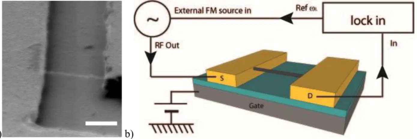
hydrofluoric acid followed by a critical point drying in CO2. Figure 1a shows a scanning electron
microscope (SEM) image of a suspended nanotube at the end of the process.
Measurements were performed in a home-made ultra high vacuum probe station (base pressure
below 2*10-10 Torr). A signal from a lock-in amplifier at low frequency (ωL) was sent to the FM input of
a radio frequency (RF) generator. We typically used ωL//2π=616.3 Hz though audio signal frequencies
were also tried. An FM signal VFM(t)=Vc*cos(ψ(t)), where ψ(t)=ωct+(ωΔ/ωL)sin(ωLt), was applied to the
frequency deviation and t the time. Finally, the low frequency signal from the drain electrode was
measured by the current input of the lock-in. In a standard FM radio, ωΔ is proportional to the amplitude
of the sound to be carried and ωL is its frequency.
a) b)
Figure 1. (a) SEM image of one of our devices with a suspended nanotube between 2 gold electrodes (scale bar 1 µm). (b) Schematic diagram of the experimental setup for FM measurements.
Measurements were carried out on 7 different devices. We swept ωc over large frequency spans
and recorded the magnitude (R) and phase (θ) of the lock-in signal for different fixed DC gate voltages.
Peaks in current were found at various frequencies. These peaks were proven to be due to the vibrations
of the nanotube by varying the DC gate voltage which tunes the frequencies of the mechanical
resonances by mechanical strains induced by electrostatic forces22,14. We also performed some
measurements with the same mixing technique as ref. 14 to check that the resonance peaks of our
sample are at the same frequency with both methods. After coarse identification of the resonances, finer
frequency scans were made to determine their exact shape (figure 2a). R showed a rather unusual form
with one central peak and two satellites while θ had abrupt and very clear 180° jumps when R was a
minimum (figure 2b). To achieve a first understanding of these forms, for example the jump in θ, we
also performed “X and Y” measurements with the lock-in, where X=Rcos(θ) is the in-phase current, and
Y=Rsin(θ) is the out-of-phase current. With an appropriate choice of the phase of the lock-in, we could
cancel the Y component to get only the resonant current in the X component (see figures 2c and 2d). R
in figure 2a has the form abs(X) of figure 2c which shows that the phase jump in the θ signal is due to
mathematics necessary for calculating these curves and thus allowing their exploitation in radio
applications.
a) b)
c) d)
e) f)
Figure 2. (a) and (b) Magnitude and phase of the lock-in current versus carrier frequency in FM mode for ωΔ/2π = 500 kHz, ωL/2π = 616.3 Hz, -9.5V of DC gate voltage, Vc = 20 mV and a time constant of
300 ms. (c) and (d): in-phase and out-of-phase lock-in current versus carrier frequency in FM mode on a
different sample for ωΔ/2π = 75 kHz, ωL/2π = 616.3 Hz, 5V of DC gate voltage, Vc = 10 mV and a time
constant of 100 ms. The solid line in (d) is a fit of the experimental data with equation 4 (Q=160, ω0/2π
mode on the sample of figures (a),(b) for m = 0.9, ωL/2π = 616.3 Hz, -9.5V of DC gate voltage, Vc = 20
mV and a time constant of 300 ms
For comparison, we also performed AM demodulation at the resonance (see figures 2e and 2d)
by applying at the drain an AM signal VAM(t)=Vc*(1+m*cos(ωLt))*cos(ωct) where m is the modulation
depth. The electromechanical signal is superimposed on a 25 pA background current and the signal is
noisier. FM demodulation is a clear improvement in terms of mechanical detection as FM systems are
better in rejecting noise than AM systems23. Indeed, noise is generally related to amplitude variation and
is nearly independent of frequency as long as the signal is not too close to DC.
In the following we will show that X in figure 2c is the derivative of the real part of the complex
Lorentzian response function of the resonator and that the cancelation of Y is a specificity of FM
detection. The source current I(Vsd,x,Vg) depends on three parameters: the source drain voltage Vsd, the
gate voltage Vg and x, the position of the middle of the nanotube perpendicular to the substrate. In our
experiment, with a fixed DC gate voltage VgDC and an AC source drain voltage V(t), the leading terms
of the current are given by a second order Taylor expansion around Vsd=0 and x=x0. x0 0 due to the
electrostatic bending toward the gate induced by VgDC :
2 0 0 0 0 ( ), ) (0, , ) (0, , ) ( ) (0, , ) ( ) ), ( ( x V x t I x I t V V x V I V x I V t x x t V I gDC gDC sd DC g DC g (1)
where δx(t) is the instantaneous mechanical displacement of the nanotube due to electrostatic actuation
and I2 is the current coming from higher order terms in the Taylor expansion responsible for the low
frequency signals that can be detected by the lock-in. The first and third terms on the right hand side are
zero because no current flows in the absence of source drain voltage, for any x0 or VgDC. The second
term gives only high frequency signals.
I2 is at the origin of the signal mixing technique that we mentioned in the introduction. Mixing in
its simplest form is the multiplication of two harmonic signals that enter a two terminal mixer device. A
characteristics. From trigonometry the output signal has a harmonic component at the difference in the
frequencies of the two incoming signals with amplitude related to the high frequency intrinsic response
of the device. So this technique can be used to shift the frequency of the input signal. For instance, if the
two incoming signals are very close in frequency, the output signal is at very low frequency and can
easily be detected.
If we just include the second order terms in I2 we get:
2 2 2 2 2 2 2 2 1/2 ( ( )) ( ) ( ) 1/2 ( x(t)) x I t x t V V x I t V V I I sd sd (2)
where for the same reason as for eq. 1 the last term is zero. The first term is the same as the one of ref.
20. For an applied AM signal, this term gives a DC rectified signal, several high frequency signals and a
signal at the modulation frequency. For FM it is useful to decompose the applied signal with the
Jacobi-Anger expansion:
cos(( -n )t) ( 1) cos(( )t)
) ( J t) cos( ) ( J Vc (t) V 1 L c L c L n c L 0 FM
n n n where Jn is the n-th Bessel function. It is straightforward to show that the square of this expression,
needed for the V(t)2 factor in (2)), has no signal at the modulation frequency ωL but still has DC and
high frequency signals. So this demonstrates that pure electrical non linearities, as used in ref. 20, cannot
demodulate an FM signal, i.e. no sound can be heard from this term in the FM mode.
Let’s now take a look at the remaining term: the electromechanical current for an FM signal. It is usually
assumed that 2I
sd/xVsd is proportional to the transconductance and to C’, the space derivative of the
capacitance between the tube and the gate, but it could also be related to a piezoresistive effect. Such
piezoresistive effects are possible either due to a strain-induced intrinsic conductance change24-26 or a
variation of the contact resistance. For generality we won’t make any assumption here about this term.
The argument of the cosine in the VFM signal can be rewritten ψ(t+Δt)=ψ(t)+ψ/tΔt where Δt is a time of the order or smaller than the time scale of the oscillator Q/ω0, where Q is the quality factor of the
The electromechanical current is only significant at the resonant frequency ω0 so we consider here ωc ~
ω0. These conditions are satisfied in our experiment, so we can consider that the oscillator is submitted
at each time t to an harmonic forcing of frequency ωi = ψ/t = ωc+ωΔ cos(ωLt), namely the
instantaneous frequency, with an additional phase term ψ(t) that is constant over the time scale of
interest. Thus in the approximation of a single mechanical degree of freedom, the complex frequency
response function of the displacement δx*(ω) is:
Q i V m V V C x i i c eff offset DC g i 0 2 2 0 2 ) ( *
where Voffset is an offset voltage due to some residual charges at zero voltage, meff is the effective mass
of the nanotube. The instantaneous mechanical displacement of the nanotubes is:
)) ( sin( )) ( * Im( )) ( cos( )) ( * Re( ) (t t x t t x t t x i i i i
Substituting this into Eq. (2) gives the low frequency term of the electromechanical current, ILFFM:
)) ( * Re( 2 / 1 2 i c sd FM LF V x V x I I
Finally a Taylor expansion of Re(δx*(ωi)) for ωΔ << ωc gives :
... ) cos( *) Re( 2 1 ) cos( *) Re( )) ( * Re( )) ( * Re( 2 2 2 2 x x t x t x L i L i c i (3)
Remarkably there is no term in sin(ωLt) and no purely electrical term with cos(ωLt). Consequently,
contrary to other detection techniques, there is no undesirable background current that interferes with the
electromechanical current. For example in a two source setup as used by all previous work14,18 there is
an additional purely electrical background current from a 2I
sd/VsdVg term. In AM detection, a similar
analysis shows that this background is superimposed on the real part of δx*(ωc). In FM detection the
2 2 0 2 2 2 0 2 0 2 0 2 2 0 2 0 2 ) )( ( 2 ) ( Q Q Q F c c c c c c (4)where F is the derivative of the real part of δx*(ω), without unnecessary multiplicative constants.
Interestingly, the zeroes of F(ωc) gives the quality factor. We fitted our data by this function (see figure
2c) and obtained a good agreement. A peculiarity of the FM signal is that the power transmitted is
independent of the value of ωΔ which follows from the identity:
1 2 n 2 0( ) 2 J ( ) J 1 n u u , where u is
any real number. As the electromechanical current is proportional to ωΔ, it should increase linearly with
ωΔ. We confirmed experimentally (see figure 3a) that the demodulated FM current follows this linear
dependence for low ωΔ before peaking at a ωΔ slightly smaller than the Lorentzian width, because of
higher order terms in equation (3). This maximum (of the order of 2I
sd/xVsdVc2Q/2ω0) is comparable
but larger by at least a factor of 2 to the signal intensity obtained by the two source mixing technique for
the same amount of power. Thus there is a non-negligible gain of signal by using FM excitation. For too
high ωΔ, the cos(ωLt) component of the current is no longer proportional to F(ωc), its zeroes move
further apart and they no longer give the quality factor directly (see figure 3a). From the experimental
data at low ωΔ, we extracted the parameter of F(ωc) and calculated numerically the value of the cos(ωLt)
component of ILFFM for various ωΔ and got an excellent agreement (see figure 3a). Finally in this regime,
detectable higher order terms implies the appearance of harmonics from the expansion of cos(ωLt)n
terms (where n is for the nth order). Each harmonic is proportional, to first order, to the nth derivative of
Re(δx*(ωi)) (see equation (3)). For ωΔ = 500 kHz, we observed up to 9 harmonics (figure 3c shows
harmonics 2, 3 and 4) and could hear clearly distinguishable noise distortion when the signal was sent to
a loudspeaker. However, for radio applications, where ωΔ < 200 kHz, our device is still in the linear
(a) (b) (c)
Figure 3. (a) (■) Absolute value of the maximum current at cos(ωLt) and () frequency difference
between F(ωc) zeroes for different ωΔ for the same parameter of figure 2 a).The solid lines are obtained
from numerical simulations. (b) In phase current versus carrier frequency for ωΔ/2π = 50 kHz (solid
line), 200 kHz (dashed line), 700 kHz (dotted line), 2 MHz (dashed doted line). (c) In phase current
versus carrier frequency for different harmonics (harmonic 2: solid line, harmonic 3: dashed line,
harmonic 4: dotted line) with ωΔ/2π =500 kHz, ωL/2π = 616.3 Hz, -9.5V of DC gate voltage, Vc = 12
mV and a time constant of 300 ms.
An important point about the cancellation of the Y component is that this detection technique is
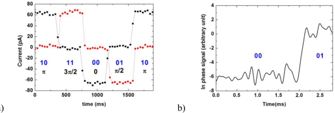
not only sensitive to the frequency ωL, but also to its phase. This is of some interest for digital data
transfer since some common modulation schemes such as QPSK (quadrature phase shift keying) uses
the phase of the signal to enhance data transmission by sending more than 1 bit at the same time. The
principle is to code, for example, 2 bits by changing the phase φ by π/2 steps. This gives 4 different
states (φ = 0 coding 00 in bits, φ = π/2 for 01, φ = π for 10 and φ = 3π/2 for 11). Experimentally, we
used an independent low frequency generator to send the cos(ωLt+φ) signal that FM modulates the
carrier frequency of the high frequency generator. We record the demodulated signal in the lock-in using
its internal source. The carrier frequency is fixed at the resonance of the nanotube. For φ = 0, we set the
phase of the lock-in, in order to have a large negative signal in X and zero in Y, then we keep constant
the phase of the lock-in and only change the phase of the external low frequency generator. So for φ =
π/2 we got zero in X and a large negative signal in Y i.e. the resonance is detected by the out of phase
component. For φ = π (respectively φ = 3π/2) we got a sign reversal in X (respectively Y) compared to φ
nanotube NEMS. The maximum transfer rate about 60 bps (bit per second) is limited here by the 30 ms
time transfer of our GPIB connection between the lock-in and the computer. To push the data transfer
rate even further we i) used a sample with a resonant electromechanical current above 1nA to lower the
time constant of the lock-in and still have a reasonable signal to noise ration and ii) did the measurement
of the current with the analog 100 kHz bandwidth output of the lock-in sent to a high speed
oscilloscope. Figure 4b shows a rise time of 200 µs with a signal to noise ration of 8 when passing from
00 to 01. Thus we have achieved a transfer rate of 10 kbps thanks to this 2 bit at a time transfer method.
This means that our device reached the requirement for the widely used GSM (global system for mobile
communication) cell phone standard where the voice is digitally transported at a 9.6 kbps rate.
a) b)
Figure 4. (a) Digital demodulation (■ in phase and out of phase component) for ωΔ/2π = 200 kHz,
ωL/2π = 616.3 Hz, ωc/2π = 112.8 MHz, -9.5V of DC gate voltage, Vc = 20 mV and a time constant of 10
ms. (b) High speed digital demodulation for ωΔ/2π = 750 kHz, ωL/2π = 7243 Hz, ωc/2π = 156.98 MHz,
9V of DC gate voltage, Vc = 20 mV and a time constant of 30 µs.
In conclusion we showed that FM and digital demodulation is possible using carbon nanotubes NEMS
in a transistor geometry. We theoretically demonstrated that the shape of the resonance peak is related to
the derivative of the real part of the response function of the resonator. With this technique, it is possible
to reduce the noise and unwanted back ground signals as well as to detect derivative of the response
function up to the ninth order. The noise reduction of FM demodulation might be useful for NEMS
applications such as ultimate mass sensing. Our device achieved a transfer rate of 10 kbps compatible
ACKNOWLEDGMENT. This work is supported by French National Agency (ANR) through
Nanoscience and Nanotechnology Program (Projects NEXTNEMS n°ANR-07-NANO-008-01), through
"Jeunes Chercheuses et Jeunes Chercheurs" Program (Project AUTONOME n°ANR-07-JCJC-0145-01)
and cluster micro-nano of the région Rhône Alpes. It was carried out within the framework of the Group
Nanowires-Nanotubes Lyonnais. The authors acknowledge the support of the "Centre Technologique
des Microstructures de l’Université Lyon 1". We thank the OMNT experts, L. Montes and G. Bremond
for fruitful discussions, P. Cremilleu and R. Mazurczyk in the Institut NanoLyon technological platform
for help in sample fabrication.
REFERENCES
(1) Gammel, P.; Fischer, G.; Bouchaud, J. Bell Labs Tech. J. 2005, 10 (3), 29.
(2) Jensen, K.; Kim, Kwanpyo; Zettl, A. Nature nanotechnology 2008, 3, 533.
(3) Treacy, M. M. J.; Ebbesen, T. W.; Gibson, J. M. Nature 1996, 381, 678.
(4) LaHaye, M. D.; Buu, O.; Camarota, B.; Schwab, K. C. Science 2004, 304, 74.
(5) Scheible, D. V.; Weiss, C.; Kotthaus, J. P.; Blick, R. H. Phys. Rev. Lett. 2004, 93, 186801.
(6) Ayari, A.; Vincent, P.; Perisanu, S.; Choueib, M.; Gouttenoire, V.; Bechelany, M.; Cornu, D.;
Purcell, S. T. Nano Lett. 2007, 7, 2252.
(7) Kis, A.; Zettl, A. Phil. Trans. R. Soc. A 2008, 366, 1591.
(8) Singh, D. V.; Jenkins, K. A.; Appenzeller, J.; Neumayer, D.; Grill, A.; Wong, H. S. P. IEEE
transactions on nanotechnology 2004, 3, 383.
(10) Chaste, J.; Lechner, L.; Morfin, P.; Feve, G.; Kontos, T.; Berroir, J.-M.; Glattli, D. C.; Happy,
H.; Hakonen, P.; Placais, B. Nano Lett. 2008, 8, 525.
(11) Appenzeller, J.; Frank, D. J. Appl. Phys. Lett. 2004, 84, 1771.
(12) Rosenblatt, S.; Lin, Hao; Sazonova, V.; Tiwari, Sandip; McEuen, P. L. Appl. Phys. Lett. 2005,
87, 153111.
(13) [1][2][3][4][5]. A.; Baumgardner, J. E.; Folk, E.; Przybysz, J. X.; Adam, J. D.; Zhang, Hong Appl.
Phys. Lett. 2006, 88, 113103.
(14) Sazonova, V.; Yaish, Y.; Ustunel, H.; Roundy, D.; Arias, T. A.; McEuen, P. L. Nature 2004,
431, 284.
(15) Witkamp, B.; Poot, M.; van der Zant, H. S. J. Nano Lett. 2006, 12, 2904.
(16) Peng, H. B.; Chang, C.W.; Aloni, S.; Yuzvinsky, T. D.; Zettl A. Phys. Rev. Lett. 2006, 97,
087203.
(17) Lassagne, B.; Garcia-Sanchez, D.; Aguasca, A.; Bachtold A. Nano Lett. 2008, 11, 3735.
(18) Chiu, Hsin-Ying; Hung, P.; Postma, H. W. Ch.; Bockrath M. Nano Lett. 2008, 12, 4342.
(19) [6]. PhD Thesis 2006, p. 67 http://www.lassp.cornell.edu/lassp_data/mceuen/
homepage/pubs.html.
(20) Rutherglen, C.; Burke, P. Nano Lett. 2007, 11, 3296.
(21) Jensen, K.; Weldon, J.; Garcia H.; Zettl, A. Nano Lett. 2007, 11, 3508.
(22) Purcell, S. T.; Vincent, P.; Journet, C.; Binh, V. T. Phys. Rev. Lett. 2002, 89, 276103.
(23) Rutledge, D. The electronics of radio, Cambridge University Press, 1999, p. 9.
(25) Minot, E. D.; Yaish, Y.; Sazonova, V.; Park, J.-Y.; Brink, M.; McEuen, P. L. Phys. Rev. Lett.
2003, 90, 156401.
(26) Stampfer, C.; Jungen, A.; Linderman, R.; Obergfell, D.; Roth, S.; Hierold, C. Nano Lett. 2006, 7,