HAL Id: cea-02349674
https://hal-cea.archives-ouvertes.fr/cea-02349674
Submitted on 5 Nov 2019HAL is a multi-disciplinary open access
archive for the deposit and dissemination of sci-entific research documents, whether they are pub-lished or not. The documents may come from teaching and research institutions in France or abroad, or from public or private research centers.
L’archive ouverte pluridisciplinaire HAL, est destinée au dépôt et à la diffusion de documents scientifiques de niveau recherche, publiés ou non, émanant des établissements d’enseignement et de recherche français ou étrangers, des laboratoires publics ou privés.
Analysis and Functionalization of 2D materials with
Electrochemical Microscopy
R. Cornut, H Casademont, T Bottein, V. Derycke, S. Campidelli, B. Jousselme
To cite this version:
R. Cornut, H Casademont, T Bottein, V. Derycke, S. Campidelli, et al.. Analysis and Functionalization of 2D materials with Electrochemical Microscopy. ELECNANO7, May 2016, Lille, France. �cea-02349674�
ElecNano7 23-25 may 2016
Lille, France
Analysis and Functionalization of 2D materials with Electrochemical
Microscopy
R. Cornut a, H. Casademont a, T. Bottein a, V. Derycke a, S. Campidelli a, B. Jousselme a
a
ACEA Saclay, IRAMIS, NIMBE (UMR 3685), LICSEN, 91191 Gif-sur-Yvette, France
2D materials such as Graphene and graphene oxide (GO) or CVD-Molybdenum Sulfide (MoS2) are attracting increasing attention from the scientific community.1,2 These materials
have outstanding properties, so that many potential applications in the fields of electronics, sensors, catalysis and energy storage are being considered.
In a previous work3 we introduced a new localized functionalization method of GO deposited on a silicon oxide surface based on its reduction at the local scale thanks to scanning electrochemical microscopy (SECM): the reducer is generated at the microelectrode, that is moved close to the substrate. The recovery of electronic conductivity upon reduction enables the selective electrochemical functionalization of patterns.
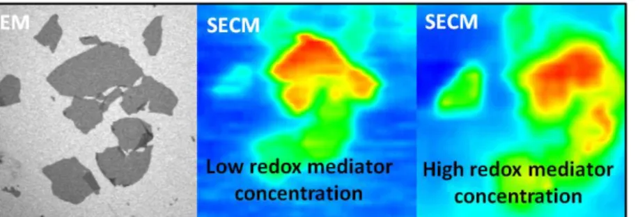
Besides, we introduced a method to evaluate at a local scale the conductivity of 2D materials with SECM.4 In addition we show how images of individual and interconnected flakes directly reveal the signature of the contact resistance between flakes in a non-contact and substrate-independent way.5 Quantitative evaluation of the parameters is achieved with the support of numerical simulations to interpret the experimental results.
Overall, these works illustrate the high potential and versatility of SECM to investigate and functionalize 2D materials.
Figure 1. Presentation of the combined SEM-SECM responses at the basis of the advanced electronic conduction characterization.5
(1) A. K. Geim; Science 2009, 324, 1530.
(2) Li, H. N. ; Shi, Y. M. ; Chiu, M. H. ; Li, L. J., Nano Energy 2015, 18, 293.
(3) Azevedo, J. ; Fillaud, L. ; Bourdillon, C. ; Noel, J-M.; Kanoufi, F.; Jousselme, B. ; Derycke, V. ; Campidelli, S. ; Cornut, R. ; J. Am. Chem. Soc., 2014, 136, 4833.
(4) Azevedo, J. ; Bourdillon, C. ; Derycke, V. ; Campidelli, S. ; Lefrou, C. ; Cornut, R.; Anal.
Chem. 2013, 85, 1812.
(5) Bourgeteau, T. ; Le Vot, S. ; Bertucchi M. ; Derycke, V. ; Jousselme, B. ; Campidelli, S. ; Cornut, R.; J. Phys. Chem. Lett, 2014, 5, 4162.