HAL Id: tel-01071694
https://tel.archives-ouvertes.fr/tel-01071694
Submitted on 6 Oct 2014
HAL is a multi-disciplinary open access
archive for the deposit and dissemination of sci-entific research documents, whether they are pub-lished or not. The documents may come from teaching and research institutions in France or abroad, or from public or private research centers.
L’archive ouverte pluridisciplinaire HAL, est destinée au dépôt et à la diffusion de documents scientifiques de niveau recherche, publiés ou non, émanant des établissements d’enseignement et de recherche français ou étrangers, des laboratoires publics ou privés.
Développement de cellules solaires à base de films
minces CZTSSe
Giovanni Altamura
To cite this version:
Giovanni Altamura. Développement de cellules solaires à base de films minces CZTSSe. Autre [cond-mat.other]. Université de Grenoble, 2014. Français. �NNT : 2014GRENY022�. �tel-01071694�
Université Joseph Fourier / Université Pierre Mendès France / Université Stendhal / Université de Savoie / Grenoble INP
THÈSE
Pour obtenir le grade de
DOCTEUR DE L’UNIVERSITÉ DE GRENOBLE
Spécialité : Physique des matériauxPrésentée par
Giovanni ALTAMURA
Thèse dirigée par Henri MARIETTE etcodirigée par Louis GRENET et Simon PERRAUD
préparée au sein du CEA INAC, Equipe Nanophysique et
Semiconducteurs (NPSC)
dans l'École Doctorale de Physique, UJF
Développement de cellules
solaires à base de films
minces Cu
2
ZnSn(S,Se)
4
Thèse soutenue publiquement le 2 Septembre 2014 devant le jury composé de :
M. Daniel BELLET
Professeur à Grenoble-INP, présidente du jury
M. Daniel LINCOT
Professeur à Chimie-ParisTech, rapporteur
M. Jean-Yves CHANE-CHING
Chercheur à l’université Paul Sabatier Toulouse, rapporteur
M. Louis GRENET
Ingénieur de Recherche au CEA Liten, encadrant
M. Simon PERRAUD
Ingénieur de Recherche au CEA Liten, co-encadrant
M. Henri MARIETTE
II
A mamma, papà,
Tony, Maurizio
e Annarita
III
“Tänka fritt är stort, men
Tänka rätt är större”
Thomas Thorild (1759-1808)
IV
Acknowledgements
First, I would like to thank all members of the examining committee of this PhD thesis. Thank you to Daniel Lincot and Jean-Yves Chane-Ching for agreeing to evaluate my work. Thank you to Daniel Bellet for agreeing to serve as president of the panel.
I still remember when in July 2011, sitting at my desk in my old office in Paris, I decided to move to Grenoble and start my PhD at CEA: now I can say that it has been the best decision I have ever made in my entire life! For that I would like to thank faithfully three persons: my thesis director Henri Mariette, and my two co-supervisors Louis Grenet and Simon Perraud. Thank you Henri for being a real teacher for me, I learned from you that most of the times things (in Physics) are not like they could appear: that there are more and more explanations and viewpoints to address the conclusions of an experiment, and that going deeply in the understanding of what I am doing is always the best solution. Thank you Louis for being by my side every time I needed: it has been very important for me to have the possibility to count on you and have your support in the development of my ideas. You taught me how to start and how to conclude an experiment, how to write a scientific paper, how to prepare an oral presentation, how to evaluate things around me the way they are evolving. Thank you Simon for being for me the main example of: scrupulousness, accuracy and organization in a workgroup and especially in my daily work. I etched in my head your phrase: “Giovanni, il faut que tu sois en peu plus rigoureux!” I promise you I will always be. You three will always be my mentors and source of inspiration!
Thank you to Emmanuelle Rouvière for welcoming me into the great family of LITEN, et for giving me the chance to express myself in this environment.
A big thank you to the photovoltaic team at LITEN: you have been part of my daily work and it has been a pleasure to spend these three years with all of you. Thank you Fred for receiving me in your Barnave domain, for sharing with me your knowledge, enthusiasm and…of course beers. Thank you Nico to teach me how to watch one step ahead, and that a patent is always around the corner when an idea pops out of the head. Thank to David, Charles and Raphael: I do not know if the right way to thank all of you does really exist! You have been the best glue between the “daily work in the office” and the “nightly work outside the office”, I hope that our friendship will last forever and I wish you guys all the best in your future! Thank you Mathieu and Jérôme to be part of these three years even when you left the office, you taught me a lot on the French street language and costumes. Thank you Hélène and Cécile for giving the feminine touch to the environment, and for everything we have shared together. Thank you Pascale and Fabrice for being always open
V
to discussions and confrontation on different themes of my work. Thank you Seb, Christine, Sévak, Pauline, Dario, Chloé, Karol and Jesus for being active part at the right moment of this experience, it is also because of you that my PhD has come to an end. I would like also to address a big thank you to MY team at INAC: in particular the continuous exchange with you of ideas and prospective has been fundamental for the success of my PhD project. A big thank to Hervé Boukari and Yoann Cure for the discussions and debates on kesterite technology. Thank you Joël Bleuse for the passion demonstrated me about optics and to how important it is in my project. Thank you to Catherine Bougerol for helping me whenever I needed you during the thesis. Thank you to Régis André for being a colleague always open and curious about my work. Thank you to Sirona Valdueza-Felip, Luca Radaelli, Anna Markhatova, Lionel Gérard, Gilles Nogues, Yann Genuist, Didier Boilot and Bruno Daudin for let me be part of your project and at the same time be part of mine. A big thank to all the other PhD students at NPSC, I wish all the best for you as well.
A big thank you is for Sergio Bernardi and Patrick Chapon for the relationship we have created in these three years: I am sure about the fact that our collaboration will not stop now.
I cannot forget all my friends that although outside my PhD environment, they are, without a doubt, the best I could even imagine. Thank you for all you have done in these three years fellas! Thank you Riccardo for everything we shared together: I should write other 150 pages to explain the weight of your influence in these years. Thank you to my “sunshine friends”: Chiara, Giada, Vera, Johnny, Marco, Clio, Carlo, Lorenzo, Eric, Caroline, Simeon, Ramona, Lia, Stefano. The moments we spent together are etched in my heart and are something that even the time cannot erase! Thank you Alice for being such a joy and delight: I promise not to stop being such a good godfather. Another big thank you is directed towards my dear friends back in Italy (Vita, Angelo, Vito, Francesco Z, Aura, Danilo, Giuseppe, Francesco D, Piero, Laura, Nunzio, Gianluca and all the others) for always supporting me although we meet twice per year since nine years now. You are my oldest friends and I will always love you.
Thank you to my Parents and my Siblings for being the universe in which my world exists. You always say that we are not perfect but the love you show me everyday overtakes the perfection!
VII
Résumé
L'objectif principal de cette thèse consiste à déterminer (et expliquer) les relations entre les conditions de synthèse des couches minces de Cu2ZnSn(Se,S)4 (CZTSSe), leurs propriétés
physiques et les performances des dispositifs photovoltaïques. Le mécanisme de formation du matériau est étudié en fonction des conditions de croissance. Le CZTSSe est synthétisé par un procédé en deux étapes, où une première étape de dépôt des précurseurs sous vide est suivie d'une seconde étape de recuit sous atmosphère de sélénium. Différents ordres d'empilement des précurseurs sont étudiés afin de comprendre la séquence de réactions qui, à partir de leur dépôt, conduit à la couche finale de CZTSSe. Le résultat de cette étude montre que le matériau final obtenu après un recuit à haute température (570°C) et de longue durée (30 min) est indépendant de l’ordre de dépôt des précurseurs, mais que les étapes intermédiaires de formation du matériau sont fortement influencées par les positions respectives des couches de cuivre et d’étain.
Les possibles implications bénéfiques de l'incorporation de sodium dans le CZTSSe sont également étudiées. Ce travail est réalisé en synthétisant la couche de CZTSSe sur différents substrats contenant diffèrents taux de sodium: de cette manière, pendant la synthèse, le sodium migre du substrat vers l'absorbeur. Après quantification du Na dans le CZTSSe juste après la croissance, le matériau est caractérisé afin d'évaluer sa qualité. Ensuite il est employé dans une cellule solaire complète pour vérifier ses propriétés photovoltaïques. Les résultats montrent que, comme dans le cas de la technologie CIGS, le sodium est bénéfique pour le CZTSSe, permettant l'augmentation de la tension à circuit ouvert et le rendement des cellules.
Le molybdène est le contact arrière le plus utilisé pour les cellules solaires à base de CZTSSe. Cependant, il a été suggéré récemment que le Mo n'est pas stable à l'interface avec le CZTSSe. En outre, aucune étude expérimentale n’a été effectuée à ce jour pour tester si les cellules solaires construites sur un autre contact arrière pourraient présenter de meilleures propriétés photovoltaïques. Ainsi, divers métaux (Au, W, Pd, Pt et Ni) sont déposés sur le Mo et testés comme contacts arrières dans les cellules solaires à base de CZTSSe. Il est démontré qu'il est possible de synthétiser des couches minces de CZTSSe de qualité quand le tungstène, l’or et le platine sont employé comme contacts arrière. Il est observé que les contacts en W et Au permettent d’augmenter le courant photogénéré, mais aussi que le Mo reste le meilleur contact arrière du point de vue du rendement de conversion photovoltaïque.
Les effets de la variation du rapport [S]/([S]+[Se]) sur les performances des cellules solaires à base de CZTSSe sont étudiés. Cette étude est effectuée par simulations des cellules solaires à base de CZTSSe, avec un ratio variable des éléments chalcogènes dans
VIII
l’absorbeur, en ayant pour objectif la détermination de la composition optimale de l’absorbeur. Les simulations conduisent à un rendement de 16,5% (avec une tension en circuit ouvert de 0,56 V, courant de court-circuit de 37,0 mA/cm2 et un facteur de forme de 79,0%) lorsque la teneur en soufre est diminué linéairement à partir du contact arrière en direction de la couche tampon. Sur la base de ces résultats, nous proposons que l'ingénierie de bande interdite avec une variation du taux [S]/([S]+[Se]) dans l'absorbeur soit un moyen efficace qui permet d'augmenter les performances des cellules solaires à base CZTSSe sans nécessiter de changer la qualité même de l'absorbeur.
IX
Scientific Production
Journal Papers
– G. Altamura, C. Roger, L. Grenet, J. Bleuse, H. Fournier, S. Perraud and H. Mariette, “Influence of sodium-containing substrates on Kesterite CZTSSe thin
films based solar cells”, MRS Proceedings / Volume 1538 / 2013.
– S. Valdueza-Felip, A. Mukhtarova, Q. Pan, G. Altamura, L. Grenet, C. Durand, C. Bougerol, D. Peyrade, F. González-Posada, J. Eymery, E. Monroy, “Photovoltaic
Response of InGaN/GaN Multiple-Quantum Well Solar Cells”, Jpn. J. Appl. Phys. 52 (2013) 08JH05.
– G. Altamura, L. Grenet C. Bougerol, E. Robin, D. Kohen, H. Fournier, A. Brioude, S. Perraud and H. Mariette, “Cu2ZnSn(S1-xSex)4 Thin Films for Photovoltaic
Applications: Influence of the Precursor Stacking Order on the Selenization Process”, Journal of Alloys and Compounds 588 (2014), 310-315
– G. Altamura, L. Grenet, C. Roger, F. Roux, V. Reita, R. Fillon, H. Fournier, S. Perraud and H. Mariette, “Alternative back contacts in kesterite
Cu2ZnSn(S1-xSex)4 thin film solar cells”, J. Renewable Sustainable Energy 6 , 011401 (2014)
– G. Altamura, L. Grenet, R. Fillon, S. Perraud and H. Mariette, “Influence of
[S]/([S]+[Se]) ratio in kesterite Cu2ZnSn(S,Se)4 solar cells: a numerical simulation approach”, manuscript in preparation.
– L. Grenet, R. Fillon, G. Altamura, H.Fournier, F. Emieux, P Faucherand, S. Perraud, “Analysis of photovoltaic properties of Cu2ZnSn(S,Se)4-based solar cells”,
Solar Energy Materials & Solar Cells 126 (2014), 135-142.
– C. Roger, G. Altamura, F. Emieux, O. Sicardy, F. Roux, R. Fillon, P. Faucherand, N. Karst, H. Fournier, L. Grenet, F. Ducroquet, A. Brioude, S. Perraud,
“Sodium-doped Mo Back Contacts for Cu(In,Ga)Se2 solar cells on Metallic Substrates : Growth, Morphology and Sodium Diffusion”, J. Renewable Sustainable Energy 6, 011405 (2014)
Conferences
– 27th European Photovoltaic Solar Energy Conference and Exhibition (September 24-28, Frankfurt / Germany), poster presentation.
– E-MRS 2013 SPRING MEETING (May 27-31, Strasbourg / France), oral presentation.
– ICMAT 2013 Material for Advanced Technologies (30 June - 5 July, Singapore), oral presentation.
– PVTC 2013 conference (May 22 - 24, Aix-en-Provence / France), oral presentation.
X
– 39th IEEE Photovoltaic Specialists Conference (June 16-21, Tampa / USA), poster presentation.
– 2013 MRS Spring Meeting & Exhibit (April 1-5, San Francisco / USA), poster presentation.
– Nanotechnology for Next Generation High Efficiency Photovoltaics Spring
International School (April 1-6, Cargèse / France), poster presentation.
– SPIE Photonics West (February 1-7, San Francisco / USA), oral presentation.
Patents
– E.N.:12 57749, Authors: L.GRENET, G. ALTAMURA, S. PERRAUD
– E.N.:13 54696, Authors: G. ALTAMURA, L.GRENET, S. PERRAUD, F. ROUX – E.N.:13 57660, Authors: L.GRENET, G.ALTAMURA, R. FILLON, S. PERRAUD
Awards and Fellowships
– Best poster award at PVTC 2013 Conference, 22-24 May, Aix-en-Provence, France – Invited Lecture at IUPAC NMS-IX 2013 Conference, 17-22 October, Shanghai, China
XII
Table of contents
1. Introduction 2
1.1. Aim of this study 3
1.2. References 4
2. State-of-the-art 7
2.1. Physics of Photovoltaics 8
2.1.1. The photovoltaic effect 8
2.1.2. Current trends in PV technology 8
2.1.3. Solar radiation 10
2.1.4. Principle 11
2.1.5. Physics of p-n junction 12
2.1.6. Current-voltage characteristics of a diode 13
2.1.7. Ideality factor 14
2.1.8. Light I-V characteristics 15
2.1.8.1. Short-circuit current 16
2.1.8.2. Open-circuit voltage 16
2.1.8.3. Fill Factor 17
2.1.8.4. Power Conversion Efficiency 17
2.1.9. Losses in solar cell 18
2.1.9.1. Series resistance 19
2.1.9.2. Shunt resistance 19
2.2. Solar cell 20
2.3. Thin film solar cell 20
2.3.1. Device structure 20
2.3.2. Possible Materials 21
2.3.2.1. Amorphous Silicon 21
2.3.2.2. Cadmium Telluride 21
2.3.2.3. Cu(In,Ga)Se2 22
2.4. Cu2ZnSn(S,Se)4 Solar cells 22
2.4.1. Introduction 22
2.4.2. Material properties 22
2.4.2.1. CZTSSe crystal structure 23
2.4.2.2. CZTSSe bandgap 28
2.4.2.3. CZTSSe defects and doping 29
XIII
2.4.2.5. CZTSSe absorption coefficient 31
2.4.3. Technological status of Cu2ZnSn(S,Se)4 solar cells 32
2.4.3.1. Vacuum techniques 32
2.4.3.2. Non-vacuum techniques 32
2.4.4. History of CZTSSe solar cells 34
2.5. References 34
3. Experimental 40
3.1. Fabrication techniques 41
3.1.1. Molybdenum back contact 41
3.1.2. Precursor deposition 41
3.1.3. Selenization 42
3.1.4. Processing of the solar cell 44
3.1.4.1. CdS buffer layer 44
3.1.4.2. Transparent conductive oxide 44
3.1.4.3. Ni/Al grids 45
3.2. Analysis techniques 45
3.2.1. Material properties 45
3.2.1.1. Scanning electron microscopy 45
3.2.1.2. Energy Dispersive X-ray Spectroscopy 46
3.2.1.3. X-ray Diffraction 47
3.2.1.4. Raman spectroscopy 48
3.2.1.5. Glow Discharge Spectroscopy 49
3.2.1.6. Photoluminescence 50
3.2.2. Cells analysis 50
3.2.2.1. Light current-voltage measurements 50
3.2.2.2. Dark current-voltage measurements 51
3.2.2.3. External Quantum Efficiency measurements 52
3.3. References 52
4. Formation mechanism of Cu2ZnSn(S,Se)4 56
4.1. Motivation 57
4.2. Two-step selenization process 57
4.2.1. Different precursor stacks 58
4.2.2. Selenization annealing 59
4.3. The effect of precursor order on film growth 60
4.3.1. Study of selenization process by SEM 61
4.3.2. Study of selenization process by EDS 61
4.3.3. Study of selenization process by Raman spectroscopy 64
XIV
4.4. Minor phases at the end of selenization process 67
4.5. Thermal considerations 68
4.6. Cu2ZnSn(S,Se)4 solar cells from different stack precursors 70
4.7. Conclusions 70
4.8. References 70
5. Sodium incorporation 74
5.1. Motivation 75
5.2. Substrates 73
5.2.1. Soda Lime Glass 75
5.2.2. Borosilicate Glass 75
5.2.3. EAGLE2000 glass 76
5.2.4. Titanium 76
5.3. Mo:Na back contact 76
5.4. CZTSSe synthesized on different substrates 77
5.5. CZTSSe characterization 77
5.5.1. Sodium concentration 77
5.5.1.1. Sodium implantation 77
5.5.1.2. Sodium incorporation in CZTSSe 78
5.5.2. CZTSSe grain size dependency on Na-content 79
5.5.3. Minor phases dependency on Na-content 81
5.5.4. CZTSSe quality dependency on Na-content 82
5.6. Cu2ZnSn(S,Se)4 solar cells on different Na-content substrates 82
5.7. Cu2ZnSn(S,Se)4 solar cells with Mo:Na back contact 84
5.8. Conclusion 86
5.9. References 87
6. New back contact in Cu2ZnSn(S,Se)4 solar cells 89
6.1. Motivation 90
6.2. Back contact deposition 90
6.3. CZTSSe synthesized on different back contact 91
6.3.1. Study of the selenization process by GDS 91
6.3.2. Study of the selenization process by XRD 92
6.3.3. Study of the selenization process by Raman 93
6.3.4. Study of the selenization process by SEM 95
6.4. Cu2ZnSn(S,Se)4 solar cells with different back contacts 96
6.5. Current improvement 98
6.5.1. Bandgap evaluation 98
6.5.2. Study of gold particles by TEM 100
XV
6.5.4. Capacitance-Voltage characteristics 102
6.6. Conclusion 103
6.7. References 104
7. Influence of [S]/([S]+[Se]) ratio in Cu2ZnSn(S,Se)4 solar cells 106
7.1. Motivation 107
7.2. Solar cell capacitance simulator (SCAPS) 107
7.3. Cu2ZnSn(S,Se)4 simulation parameters 107
7.3.1. Contacts 107
7.3.2. Solar cell parameters 108
7.3.3. Defects in Cu2ZnSn(S,Se)4 absorber 110
7.4. Cu2ZnSn(S,Se)4 solar cells with different [S]/([S]+[Se]) ratio 112
7.4.1. Linear variation of the chalcogens gradient 112
7.5. Conclusions 117
7.6. References 118
8. Conclusions & recommendations for further studies 121
8.1. Works carried out 122
XVI
List of figures
Figure 1: Examples of solar cell applications: (a) building integration, (b) space, (c) plants, (d) nomad
Figure 2: Solar irradiance spectrum above atmosphere and at Earth surface.
Figure 3: p–n junction in thermal equilibrium with zero-bias voltage applied. Donor atoms (blue particles), acceptor atoms (green particles), electrons (red particles), holes (violet particles).
Figure 4: Static I-V characteristics of a diode
Figure 5: Model and I-V curve of a solar cell under illumination.
Figure 6: Graph of the FF of the solar cell: the green square is derived from the maximum power point (Vmp, Imp), the yellow square is identified by (Voc, Isc)
Figure 7: Solar cell model including parasitic resistances.
Figure 8: Influence of Rs on photovoltaic characteristics under illumination.
Figure 9: Influence of Rsh on photovoltaic characteristics under illumination.
Figure 10: Example of solar cell.
Figure 11: Two possible configurations for thin film solar cells: substrate (left side) and superstrate (right side).
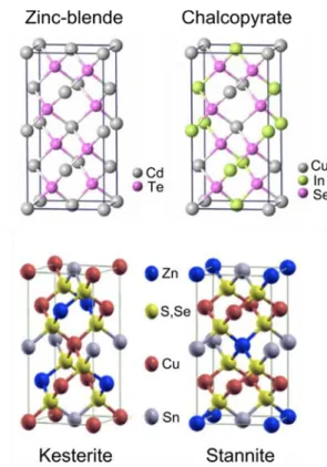
Figure 12: Formation of stoichiometric I2–II–IV–VI4 compounds can be achieved by a sequential replacement of cations.
Figure 13: Ternary composition diagram showing the position of stoichiometric CZTSSe [19].
Figure 14: Ternary phase diagram adapted from reference [19], showing the expected secondary phases at 400°C.Figure 13: Crystal structure representation of binary, ternary and quaternary compounds.
Figure 15: Ternary phase diagram defining the compositional labels used throughout this text.
XVII
Figure 17: Relationship between the crystallographic positions of cations in stannite, kesterite, and disordered-kesterite structures.
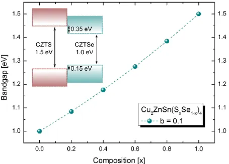
Figure 18: Cu2ZnSn(SxSe1-x)4 bandgap variation as function of the composition (x). In the inset the Type I band alignment between CZTS and CZTSe.
Figure 19: Calculated defect formation energy as a function of the Fermi energy for a Cu-poor and Zn-rich CZTSSe, taken from Ref 14.
Figure 20: The calculated chemical-potential stability diagram of pure CZTS, taken from Ref 11.
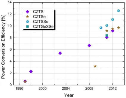
Figure 21: Evolution of the record PCE of CZTSSe solar cells as a function of years. Figure 22: Schematic of the precursor stack prior to selenization process.
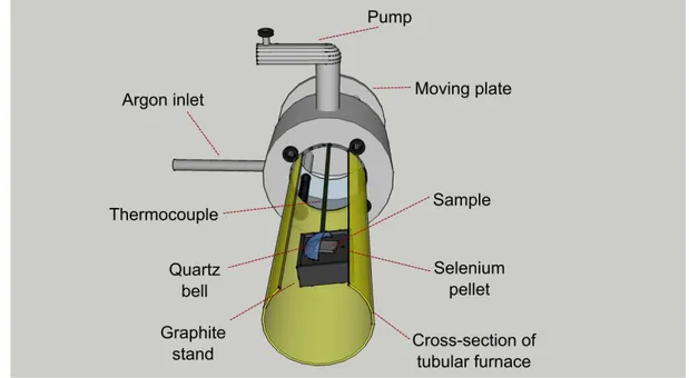
Figure 23: Cross-section of the tubular furnace employed for selenization process.
Figure 24: COMSOL simulation of temperature profile as function of the sample thickness. Figure 25: CZTSSe-based thin film solar cell.
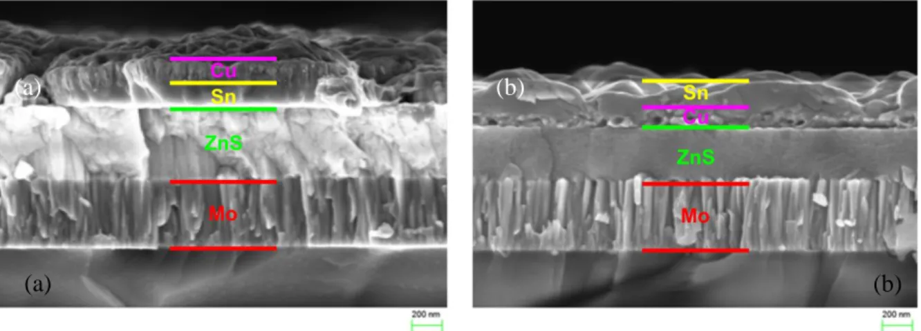
Figure 26: (a) Cross-section view of a as-annealed CZTSSe layer synthesized from a ZnS(480 nm)/Cu(180 nm)/Sn(240 nm) stack of precursors. (b) Top view of the same layer. Figure 27: (a) Cross-section EDS analysis of a as-annealed CZTSSe layer synthesized from a ZnS(480 nm)/Cu(180 nm)/Sn(240 nm) stack of precursors. (b) Top EDS of the same layer.
Figure 28: Raman spectra of pure CZTS and CZTSSe with 90% selenium layers. Main peaks of CZTS and CZTSe [15] are reported.
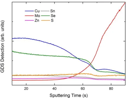
Figure 29: GDS spectrum of CZTSSe material synthesized on Mo.
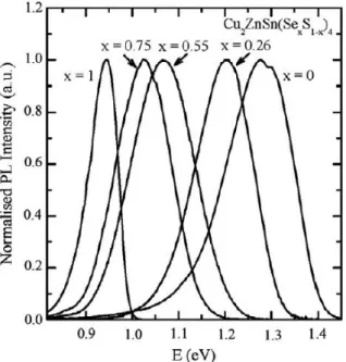
Figure 30: Normalized low-temperature photoluminescence spectra of the CZTSSe from Ref. 15.
Figure 31: The olive curve is a typical dark I-V characteristic. The wine dashed curve shows the same device without the parasitic resistances (Law Shockley). The colored areas indicate where the different parameters are extracted: Rsh (yellow), n and I0 (red) and Rs
(green).
Figure 32: External quantum efficiency of a typical Mo|CZTSSe|CdS|TCO.
Figure 33: SEM images of different precursor stacks before annealing: stack A (a) and stack B (b).
XVIII
Figure 34: Grazing incidence XRD spectra of Stack A(a) and Stack B(b) before the selenization process. The diffraction peaks are indexed utilizing the International Center for Diffraction Data for Cu5Sn6 (01-072-8761), Cu (00-004-0836), Sn (03-065-0296).
Figure 35: Temperature profiles of the samples which underwent selenization at 350°C, 450°C and 570°C (with and without the thermal plateau).
Figure 36: SEM images showing the formation of CZTSSe at different steps in the selenization process of Stack A: (a) after selenization at 350°C, (b) after selenization at 450°C, (c) after selenization at 570°C, (d) after selenization at 570°C with a 30 minute thermal plateau.
Figure 37: SEM images showing the formation of CZTSSe at different steps in the selenization process of Stack B: (a) after selenization at 350°C, (b) after selenization at 450°C, (c) after selenization at 570°C, (d) after selenization at 570°C with a 30 minute thermal plateau.
Figure 38: Cross-section EDS profiles of stack A selenized at 350°C (a) and 570°C – 30min (c); cross-section EDS profiles of stack B selenized at 350°C b) and 570°C – 30min (d). All statistical errors are twice the confidence limit. The yellow line in each image is the starting point for the calculation of [Zn]/[Sn], [Cu]/([Zn]+[Sn]) and [S]/([S]+[Se]) ratios shown in Table 2. The Zn-rich phase on the left of the black line is discarded in the composition calculations.
Figure 39: Compositional ratio at different steps of the selenization process of Stack A(a) and Stack B(b). Results are obtained from top-view from EDS measurements at 25kV. Values for the first steps have to be considered carefully because of the strong inhomogeneity of the layers.
Figure 40: CZTSSe density of stack A and B at the end of selenization process.
Figure 41: Raman spectra of the CZTSSe films at different temperatures for Stack A (a) and Stack B (b). The sharp peak at 355 cm-1 for CZTSSe spectrum at 570°C (green line in Stack B) is considered as an artifact of the measurement, and not indicative of the sample. Figure 42: GDS spectra of Stack A: (a) 350°C, (b) 450°C, (c) 570°C, (d) 570°C - 30min. Figure 43: GDS spectra of Stack B: (a) 350°C, (b) 450°C, (c) 570°C, (d) 570°C - 30min. Figure 44: Model illustrating the strong interaction between Sn and chalcogens as compared to the one between chalcogens and Cu; this picture tends to explain qualitatively the different intermediate states which occur during the annealing process of stack A (a) and B (b).
Figure 45: Model of the beveled and polished CZTSSe with an angle of 1 degree. The six points (A:F) represent the location point of Raman analysis.
XIX
Figure 46: Raman spectra of beveled CZTSSe from stack A (a) and B (b).
Figure 47: Thermodynamic simulations of the reactions of copper and tin with chalcogens: Sn + S ↔SnS (a), Sn + Se ↔SnSe (b), Cu + S ↔CuS (c), Cu + Se ↔CuSe (d).
Figure 48: PV performances statistical study of 18 solar cells from different precursor stacks.
Figure 49: Back contact bilayer Mo:Na|Mo.
Figure 50: Na concentration measured by SIMS for CZTSSe on different Mo-coated SLG (a) and BS (b). O, Cu, Zn, Sn, Se, S, Mo, Si concentrations are in arbitrary units.
Figure 51: SIMS profile measurement on CZTSSe starting from different ZnS precursor thickness. Schematic of the precursor stack prior to selenization process with different ZnS thicknesses are shown in the insets: 340 nm (a), 400 nm (b), 280 nm (c), 340 + 60 nm double layer (d).
Figure 52: XRD spectra for CZTSSe on different Mo-coated glasses.
Figure 53: SEM images showing the CZTSSe synthesized on Mo-coated: (a) SLG (high Na-content), (b) BS (low Na-content).
Figure 54: Raman spectra for CZTSSe on different Mo-coated glasses. Figure 55: PL spectra for CZTSSe on different Mo-coated glasses.
Figure 56: Current-voltage measurements under illumination (simulated AM1.5 spectrum, 100 mW/cm²) of Al:ZnO/i-ZnO/CdS/CZTSSe/Mo solar cells synthesized on SLG (blue boxes) and BS (orange boxes).
Figure 57: Dark current-voltage measurements of Al:ZnO/i-ZnO/CdS/CZTSSe/Mo cells synthesized on SLG (blue boxes) and BS (orange boxes).
Figure 58: Light current-voltage measurements of Al:ZnO/i-ZnO/CdS/CZTSSe/Mo/Mo:Na cells synthesized on SLG (blue boxes), BS (orange boxes), VSS (fuchsia) and Ti (violet). Figure 59: Light current-voltage measurements of Al:ZnO/i-ZnO/CdS/CZTSSe/Mo cells synthesized on SLG (blue boxes), BS (orange boxes), VSS (fuchsia) and Ti (violet).
Figure 60: Back contact bilayer.
Figure 61: GDS spectra of CZTSSe synthesized on Mo (CZTSSe|Mo) (a), Au (CZTSSe|Au) (b), W (CZTSSe|W) (c), Pt (CZTSSe|Pt) (d), Pd (CZTSSe|Pd) (e), Ni (CZTSSe|Ni) (f).
Figure 62: XRD patterns of CZTSSe synthesized on Mo (CZTSSe|Mo), Au (CZTSSe|Au), W (CZTSSe|W), Pt (CZTSSe|Pt). Patterns are shifted vertically and the x-axis is cut
XX
between 60 and 85 degrees for clarity. The inset shows a zoom on CZTSSe|W in the range 85-90 degrees.
Figure 63: XRD patterns of PtSe2.
Figure 64: Raman spectra of CZTSSe synthesized on Mo (CZTSSe|Mo) (top-left), Au (CZTSSe|Au) (top-right), W (CZTSSe|W) (bottom-left), Pt (CZTSSe|Pt) (bottom-right). The inset in the bottom-right of Fig. 61d shows the Raman spectrum of PtSe2.
Figure 65: Raman spectrum of PtSe2.
Figure 66: Top-view SEM image of CZTSSe|Pt.
Figure 67: SEM images of Al:ZnO/i-ZnO/CdS/CZTSSe/BC/Mo solar cells synthesized on Au (CZTSSe|Au) (a), W (CZTSSe|W) (b), Pt (CZTSSe|Pt) (c). The inset in Fig. 64a shows the SEM image of gold particles after selenization process.
Figure 68: Schematic of Al:ZnO/i-ZnO/CdS/CZTSSe/BC/Mo solar cells.
Figure 69: Current-voltage measurements under illumination (simulated AM1.5 spectrum, 100 mW/cm²) of Al:ZnO/i-ZnO/CdS/CZTSSe/BC/Mo solar cells.
Figure 70: Dark current-voltage measurements of Al:ZnO/i-ZnO/CdS/CZTSSe/BC/Mo solar cells.
Figure 71: External quantum efficiency measurements on best performing CZTSSe solar cells with Mo-, Au-, W-back contacts. Bandgaps Eg are deduced via linear extrapolation of the low energy slope of the EQE. The inset shows EQE spectrum of CZTSSe|W solar cell divided by the EQE spectrum of CZTSSe|Mo solar cell.
Figure 72: The bandgap energies extracted from the Tauc plot.
Figure 73: Cross-sectional EDS analysis of CZTSSe|Au performed in a TEM. Figure 74: Schematic of COMSOL simulation.
Figure 75: COMSOL simulations of electromagnetic field gain due to gold particles resonance with different radius.
Figure 76: Net charge carrier profile extracted from C – V characteristics of CZTSSe|Mo and CZTSSe|W solar cells at 300 K. The C – V is performed using 100-mV, 100-kHz ac excitation with dc bias from 0.2 to – 3 V.
Figure 77: Cliff-like and spike-like alignment respectively at CZTS|CdS and CZTSe|CdS interface.
Figure 78: Composition graph of CZTSSe absorber layer. The CZTSSe absorber thickness (L) is 1.2 µm.
XXI
Figure 79: PV characteristics variation of Mo | CZTSSe | CdS | i-ZnO | ZnO:Al solar cell where the CZTSSe absorber has a linear variation of the [S]/([S]+[Se]) ratio as function of depth. PCE/% (a), FF/% (b), Voc/Volt (c), Jsc/(mA/cm2) (d), the white star indicates the best performing solar cell.
Figure 80: Graphical representation of the band alignments within different CZTSSe solar cells in the dark: CZTS (orange line), CZTSe (red dotted line), bandgap decreasing from Mo to CdS (purple line), bandgap decreasing from CdS to Mo (black line).
Figure 81: J-V characteristics of the best-performing Mo | CZTSSe | CdS | i-ZnO | ZnO:Al solar cell. CZTSSe absorber has a linear variation of the [S]/([S]+[Se]) ratio as function of depth (inset).
Figure 82: Voc losses variation (in Volt) of Mo | CZTSSe | CdS | i-ZnO | ZnO:Al solar cell
where the CZTSSe absorber has a linear variation of the [S]/([S]+[Se]) ratio as function of depth.
XXII
Symbols & Acronyms
Definition
Abbreviation
Thin Film TF
Photovoltaics PV
Crystalline Silicon c-Si
Amorphous Silicon a-Si
CuInxGa1-xSe2 CIGS
Cu2ZnSn(SxSe1-x)4 CZTSSe
Cu2ZnSnS4 CZTS
Cu2ZnSnSe4 CZTSe
European Photovoltaic Industry
Association EPIA Air Mass AM Valence Band VB Conduction Band CB Photon Energy Eph Bandgap Energy Eg Donor concentration ND Acceptor concentration NA Boltzmann constant k Temperature T Electron concentration n Hole concentration p Compensation ratio Δ
Intrinsic carrier concentration ni
Space charge region SCR
Electric field ⃗
Current density J
XXIII
Dark saturation current I0
Ideality factor n Dielectric permittivity Saturation velocity vs Time t Generation rate Gn Recombination rate Rn
Carrier diffusion length L
Carrier lifetime τ
Physical vapor deposition PVD
Soda lime glass SLG
Back contact BC
Chemical bath deposition CBD
Transparent conductive oxide TCO
Cadmium Sulphide CdS
Zinc Oxide ZnO
Aluminum doped Zinc Oxide Al:ZnO
Scanning Electron Microscopy SEM
Energy Dispersive X-ray Spectroscopy EDS/EDX
X-Ray Diffraction XRD
Full Width at Half Maximum FWHM
Glow Discharge Spectroscopy GDS
Photoluminescence PL
Current-voltage measurements I-V
Open circuit voltage Voc
Short circuit current Jsc
Fill Factor FF
Power Conversion Efficiency PCE
Series resistance Rs
Shunt resistance Rsh
External Quantum Efficiency EQE
XXIV
Borosilicate glass BS
EAGLE2000 glass VSS
Secondary Ion Mass Spectrometry SIMS
Capacitance-voltage measurements C-V
Transmission electron microscopy TEM
Charge carrier density N
Vacuum permittivity ɛ
Relative material permittivity ɛ0
Space charge region width w
Diffusion voltage VD
Photogenerated current Jph
Surface recombination velocity SRV
Electron effective mass Hole effective mass
Electron band mobility μe
Hole band mobility μh
Electron affinity xe
Effective density of states in conduction
band Nc
Effective density of states in valence band Nv
Trap density Ndef
Capture cross-section σ
Minority carrier lifetime τ
Thermal velocity of electrons vth
Defect distribution WG
Chalcogens ratio at the CZTSSe|CdS
interface s
Chalcogens ratio at the Mo|CZTSSe
interface t
Reference current density Joo
Back surface bandgap BSG
2
Chapter 1
Introduction
Outline
1.1 Aim of this study
3
1.1 Aim of this study
Due to the decrease of system installation costs and increasing industry experience, photovoltaics (PV) will become an increasingly economically advantageous source of electricity. Around 200 GW in 2020 and 2 TW in 2050 of cumulated PV capacity is predicted to be installed globally [1]. These volumes will have a major impact on PV technologies in terms of resources and production.
Thin-film PV (TFPV) technology has more than 10% of this volume share, expecting to increase in the next ten years [1]. Despite the good results of TFPV and the increasing confidence in this technology, some drawbacks concerning the materials employed are highlighted. Some of the materials investigated are either expensive or toxic: arsenic, cadmium, gallium, germanium, indium, and tellurium. An evaluation of the literature does not picture a clear framework on this subject [2-3]. Nevertheless, despite the differences in the conclusion, the common thought is that a potential risk to TFPV development is due to the scarcity of some elements.
Cu2ZnSn(SxSe1-x)4 (CZTSSe) material is a promising candidate for low-cost and
high-efficiency thin film solar cells. Compared to other technologies CZTSSe offers the advantage of containing no critical chemical elements. This key aspect joined to its optical properties makes possible to foresee a photovoltaic thin film technology scalable at several GW/year [4].
Many groups have focused on elaborating such materials in the past few years, using vacuum [5-6] or non-vacuum techniques [7-8], either one [6] or two-step process [5-8]. The best performances for CZTSSe-based solar cells are obtained at IBM Watson (USA) with a power conversion efficiency of 12.6%. [9]
The research of a trade-off between high performances and low processing cost CZTSSe has recently driven the attention of the scientific community. In order to become very interesting for production at industrial level, CZTSSe solar cell performances must be certainly improved. In this manuscript, different ways to improve CZTSSe solar cells are investigated. The aim of this work is firstly to better understand the CZTSSe thin film synthesis mechanism in a two-step selenization process, and secondly to study the influence of different parameters, as the bandgap of the absorber and the back contact, on the photovoltaic performances of the CZTSSe solar cell.
4
In the following, a brief description of the structure of this thesis and the main contents is given.
Chapter 2 illustrates the state-of-the-art of CZTSSe thin film technology. Starting from describing the physics of solar cells, an outlook on the different thin film technologies is taken, followed by a detailed description of CZTSSe solar cell background.
Chapter 3 describes the experimental work carried out to fabricate CZTSSe absorbers and the various techniques useful to characterize the material from a physical, morphological, optical and electrical point of view.
In Chapter 4 a study of CZTSSe formation mechanism is reported. Chapter 5 deals with the influence of sodium in CZTSSe solar cells.
Chapter 6 reports experimentally the effects of different back contacts on the performances of CZTSSe solar cells.
In Chapter 7 the effects of [S]/([S]+[Se]) ratio tuning on CZTSSe based solar cell performances have been studied by solar cell capacitance simulator (SCAPS) to find out the optimum absorber composition.
This work is completed with a summary and a brief outlook for the further improvement of solar cell performance.
1.2 References
[1] A. Jäger-Waldau, Publication Office of the European Union, ISSN: 1018-5593 [2] A. Feltrin, A. Freundlich, Renewable Energy, 33 (2008), pp. 180-185
[3] V.M. Fthenakis, Renewable and Sustainable Energy Reviews, 8 (2004), pp. 303-334 [4] H. Katagiri, K. Jimbo, S. Yamada, T. Kamimura, W.S. Maw, T. Fukano, T. Ito,T. Motohiro, Solar cell without environmental pollution by using CZTS thin films, Proceedings of Photovoltaic Energy Conversion Conference Vol. 3 (2003).
[5] L. Grenet, S. Bernardi, D. Kohen, C. Lepoittevin, S. Noel, N. Karst, A. Brioude, S. Perraud, H. Mariette, Solar Energy Materials and Solar Cells 101 (2012) 11-14.
5
[6] I. Repins, C. Beall, N. Vora, C. De Hart, D. Kuciauskas, P. Dippo, B. To, J. Mann, W. C. Hsu, A. Goodrich, R. Noufi, Solar Energy Materials and Solar Cells 101 (2012) 154-159.
[7] K. Wang, O. Gunawan, T. Todorov, B. Shin, S. J. Chey, N. A. Bojarczuk, D. Mitzi, S. Guha, Applied Physics Letters, 97 (2010), 143508.
[8] T. Todorov, O. Gunawan, S.J. Chey, T.G. De Monsabert, A. Prabhakar, D.B. Mitzi, Thin Solid Films 519 (2011) 7378-7381.
[9] W. Wang, M. T. Winkler, O. Gunawan, T. Gokmen, T. K. Todorov, Y. Zhu, D. B. Mitzi, Adv. Mater., doi: 10.1002/aenm.201301465
7
Chapter 2
State-of-the-art
Outline 2.1 Physics of Phtovoltaics 2.1.1 Photovoltaic effect2.1.2 Current trends in PV technology 2.1.3 Solar radiation
2.1.4 Principle
2.1.5 Physics of p–n junction
2.1.6 Current-voltage characteristics of a diode 2.1.7 Ideality factor
2.1.8 Light J-V characteristics 2.1.8.1 Short-circuit current
2.1.8.2 Open-circuit voltage 2.1.8.3 Fill Factor
2.1.8.3 Power Conversion Efficiency 2.1.9 Losses in solar cells
2.1.9.1 Series resistance 2.1.9.2 Short resistance
2.2 Solar cells
2.3 Thin film solar cells
2.3.1 Device structure 2.3.2 Possible materials
2.3.2.1 Amorphous Silicon 2.3.2.2 Cadmium Tellurate 2.3.2.3 Cu(In,Ga)Se2
2.4 Cu2ZnSn(S,Se)4 solar cells
2.4.1 Introduction 2.4.2 Material properties
2.4.2.1 CZTSSe crystal structure 2.4.2.2 CZTSSe bandgap
2.4.2.3 CZTSSe defects and doping
2.4.2.4 CZTSSe phase formation: parasitic secondary and ternary phases 2.4.2.5 CZTSSe absorption coefficient
2.4.3 Technological Cu2ZnSn(S,Se)4 synthesis
2.4.3.1 Vacuum techniques 2.4.3.2 Non-vacuum techniques 2.4.4 History of Cu2ZnSn(S,Se)4 solar cells
8
2.1 Physics of Photovoltaics
2.1.1 The photovoltaic effect
The origin of the word “photovoltaic” is made up from the Greek word phos (light), and
voltaic (electrical) from the name of Italian physicist Alessandro Volta. The physical basis
for photovoltaics is the “photovoltaic effect”. An appropriate definition of the photovoltaic effect is the direct conversion of light into electricity.
The term “solar cell” is employed to describe a device, which is able to convert the energy of the sun (light) into electrical energy.
The first observation of the photovoltaic effect (1839) is attributed to the French physicist Edmond Becquerel. He discovered that exposing to light two copper plates immersed in a solution, it is possible to produce a continuous flow of current. After that, an American engineer called Charles Fritts produced the first selenium-based solar cell (1883). However, the efficiency of Fritts’s cell was less than 1% which was not enough to justify it as a practical power source due to the cost of gold contacts.
1954 was the beginning of silicon technology for PV. It was discovered at Bell Labs that a silicon p-n junction could convert 6% of the incoming sunlight into electrical energy. In 1958, silicon solar panels were included on the American spacecraft Vanguard I. Hoffmann Electronics increased the efficiency to 14% and soon a market niche for silicon solar cells was discovered (1960). In the following 50 years, the global PV production has reached over 140 MW. The 21th century sees above all the ripeness of the thin film, dye-synthesized, and multijunction solar technology [1].
2.1.2 Current trends in PV technology
Renewable energy as photovoltaics is one of the alternatives to the “conventional” energy as nuclear, hydro, and coal. Nuclear has the 15% in world production of electricity. France, Japan, and USA depend on nuclear power plants (75%, 30%, and 19% respectively) in their whole energy resources [2-3]. A lot of countries, like Germany and Japan, are gradually switching to renewable energy as photovoltaics in order to reduce risk factor of nuclear energy. Total energy capacity of the world is 4742 GW in which the share of the solar energy was 37 GW in 2010 (0.78%) [3]. In 2009, the new installation of solar energy was
9
7.1 GW that was more than doubled in 2010 (17.5 GW). The top 10 companies such as Q-cells, Sharp, Suntech, Keyocera, First Solar, Motech, Solar World, Jasolar, Yingli, and Sanyo share the almost totality of the market.
It is possible to design PV power plants of several hundred MW for different applications. Some examples are shown in Figure 1.
Since its emergence thin film photovoltaics (TFPV) take on two difficult challenges: (i) to compete with silicon based PV in terms of power conversion efficiency and manufacturing costs, (ii) to contain only earth-abundant and non-toxic materials without severe degradation in the long term. Moreover as long as crystalline silicon (c-Si) solar PV manufacturing costs decreases, TFPV solar cells will remain in the small minority. In recent years, TFPV technology has experienced rapid growth and achieved significant technological advances, consolidating its place in the solar market. In 2012, TFPV represented approximately 10% of the global PV market (28.4 GW) [4].
From a physical point of view, the advantages of TF solar cells are to have a direct band gap, a high absorption coefficient which allow absorbing the majority of the solar spectrum using only few microns of materials, and reduced sensitivity to recombination at grain boundaries. Moreover, from a technological point of view, they either permit to decrease fabrication costs by exploiting manufacturing actions like roll-to-roll, or permit the usage of flexible substrates, and monolithic interconnections.
In thin film solar cells family, chalcogenide-based solar cells as Cu(In,Ga)Se2, CdTe and
Cu2ZnSn(S,Se)4 are the best candidates potentially reduce manufacturing cost of solar
energy. Recently, First Solar Company proclaimed that the current cost of electricity by its CdTe solar panel is 0.70 $/W and aims to develop solar cells at the cost of 0.5 $/W [4].
10
Figure 1: Examples of solar cell applications: (a) building integration, (b) space, (c) plants, (d) nomad
2.1.3 Solar radiation
Solar radiation is comparable to the one of a black body at 5800 °K [5]. Sunlight passes through the atmosphere, but scattering and absorption processes attenuate it. Solar irradiance spectrum occurs over a wide range of energies (or wavelengths).
The Air Mass (AM) is the path length which light takes through the atmosphere, and is useful to quantify the reduction in the power of light when it is absorbed by the atmosphere. The Air Mass is defined as:
(eq. 1)
where θ is the angle from the vertical (zenith angle). When the sun is directly perpendicular to Earth surface, AM is 1. The standard spectrum at the Earth's surface is called AM1.5G, (the G stands for global): the AM1.5G spectrum (θ = 48.2°) has been normalized to give 1 kW/m2. This spectrum is the normalized flux used to measure the performance of cells in laboratories. The standard spectrum outside the Earth's atmosphere is called AM0, because
11
the light does not overcome the atmosphere barrier. This spectrum is typically used to predict the expected performance of cells in space. Both AM0 and AM1.5G spectra are compared in Figure 2.
Figure 2: Solar irradiance spectrum above atmosphere and at Earth surface.
2.1.4 Principle
Photovoltaics allow generating electrical power by converting solar radiation. Physics of photovoltaics is based on the optical and electrical properties of semiconductors. When a photon (hʋ) with energy higher than the bandgap of the semiconductor is absorbed, an electron-hole pair is created. This means that an electron is promoted from the valence band (Ev) to the conduction band (Ec) leaving a hole behind. This pair needs to be separated then by electric field in order to avoid recombination: this field is provided by a p-n junction (see 2.1.5) which is the core of a photovoltaic device. A photon hitting on the surface of a semiconductor could be either reflected from the surface, absorbed in the material or transmitted throughout the material itself. In the case of PV devices, photons which are not absorbed (thus reflected or transmitted) are typically considered as a loss since they do not
12
generate power. Considering the energy of the photon and the bandgap of the semiconductor it is possible to establish if a photon is absorbed or transmitted:
Eph < EG: photons with energy Eph less than the band gap EG are transmitted
Eph = EG: photons with energy Eph equal than the band gap are absorbed and can create an electron hole pair.
Eph > EG: photons with energy higher than the band gap are also absorbed. However, for PV applications, part of the energy of these photons is released since electrons quickly thermalize down to the Ec lower energy states.
2.1.5 Physics of p-n junction
In a doped semiconductor the more plentiful carriers are named “majority carriers”, while the less abundant carriers are named “minority carriers”. Majority carriers are electrons (holes) in n-type semiconductors (p-type semiconductors). Minority carriers are electrons (holes) in p-type semiconductors (n-type semiconductors). At equilibrium, the product of the majority and minority carrier concentration is a constant:
(eq. 2)
where ni is the intrinsic carrier concentration, n0 and p0 are the electron and hole equilibrium carrier concentrations.
When an n-type and a p-type semiconductor are put in contact, a p-n junction is formed between the two materials. This event is the same in the case of homo-junctions or hetero-junctions. Once the two semiconductors are in contact, electrons from the n-region near the junction interface diffuse in the p-region leaving donor atoms electrically unshielded by the majority carriers. In the same way, holes from the p-region near the interface diffuse in the n-region, leaving acceptors unshielded behind. This phenomenon is called “diffusion”. The region nearby the p–n interface, common at the two semiconductors, which lost its neutrality and become actively charged, is called the “space charge region” (SCR). The rest of the two semiconductors which is not influenced by the metallurgical junction is called “quasi-neutral region” (QNR). The consequence of the formation of the SCR is an
13
electric field ( ⃗ ) which fights the diffusion for both electrons and holes. ⃗ will superimpose on the random movement of carriers accelerating holes in the same direction of the field and electron in the opposite. This phenomenon is called “drift”. When an equilibrium condition is reached, a potential difference (VD) is formed across the p-n junction. A schematic of the p-n junction is shown in figure 3.
Figure 3: p–n junction in thermal equilibrium with zero-bias voltage applied. Donor atoms (blue particles), acceptor atoms (green particles), electrons (red particles), holes (violet particles).
2.1.6 Current-voltage characteristics of a diode
The metallurgical junction introduced in the previous paragraph is the starting point to build a diode. In fact, the diode is a p-n junction connected to two contacts.
It is possible to describe the diode current-voltage (I-V) characteristics (Figure 4), though the following equation:
14
where I is the net current flowing through the diode, I0 is the dark saturation current, V is the applied voltage across the diode, n is the diode ideality factor, k is the Boltzmann constant, and T is the temperature.
Figure 4: Static I-V characteristics of a diode
I0 is defined as:
(
) (eq. 4)
I0 is the diode saturation current which is activated by the activation energy EA and is the diode leakage current in the absence of light. EA is the energy of the dominant recombination mechanism. I00 is called “reference current” which is only weakly temperature dependent. The n moderates the voltage dependence of the current density[6].
2.1.7 Ideality factor
The ideality factor (n) is typically measured from the slope of the dark I-V characteristics. In ideal solar cell, the ideality factor is as much as possible close to one. Different magnitudes of n indicate that a specific recombination mechanism is dominant. Thus the variation of the ideality factor allows evaluating the type of recombination in solar cells.
15
2.1.8 Light I-V characteristics
When a solar cell is illuminated under solar spectrum, additional electron-hole pairs are created giving rise to the so-called photogenerated current (Iph) which could be model as a current generator in parallel to the diode (Figure 5). Iph which is given by the product of the carrier generation function G(z) and the collection probability ƞc(z,V):
∫ (eq. 5)
where q is the elemental charge, and A is the surface of the solar cell. The "collection probability" (ƞc) is defined as the probability that a carrier generated by the absorption of a photon in a certain region of the p-n junction is collected. Collection probability is max in the SCR as the electric field effectively separates the electron-hole pairs. In QNR, diffusion is the dominant mechanism. In these areas only carriers generated at a distance from the SCR which is less than the minority carrier diffusion length (Ln,p) can be collected. Ln,p is the average distance a carrier can travel from the point where it is created until it recombines.
Generally, one of the two components of the junction (n or p) is used as a light absorber material in single solar cell. For this reason photovoltaic cells are designed with an absorber layer much thicker than the other layer forming the junction [6].
Iph has the effect of shifting down the I-V characteristics into the fourth quadrant (Figure 5). When a cell is light irradiated, equation 3 (diode law) needs to be modified by adding the photogenerated current, so the output current becomes:
16
Figure 5: Model and I-V curve of a solar cell under illumination.
2.1.8.1 Short-circuit current
The Isc term in Fig. 5 is named “short-circuit current” defined as the current through the solar cell when the terminals are in short circuit (the voltage across the solar cell is zero). It is one of the figures of merit of a solar cell. By definition, Isc is identical to Iph(0). The typical factors influencing Isc are the light intensity, the optical properties of the cell, the thickness of the p-n junction, and the collection probability [6].
2.1.8.2 Open-circuit voltage
Another figure of merit of solar cell is the so-called “open-circuit voltage” (Voc): which is the voltage at the output of the cell when no load is connected. In this case the output current is zero (I=0), so the Voc can be calculated from equation 6 as:
( ) (eq. 7)
From equation 4, Voc can be reformulated as:
17
Equation 8 shows that Voc depends on both I00 and Iph. The variations of I0 depend on recombination inside the solar cell, thus Voc variations also depend on the amount of recombination in the solar cell.
2.1.8.3 Fill Factor
The fill factor (FF) is the third figure of merit introduced in this chapter. It is defined as the ratio between the square drawn by the values of the current (IMP) and voltage (VMP) of the cell resulting in its maximum power point (PMP=VMP×IMP), and the square given by the product Voc×Isc (Figure 6):
(eq. 9)
An ideal solar cell has a FF as closer as possible to one. In fact FF increases along with
VMP and IMP approaching respectively Voc and Isc. To do that, it is mandatory to decrease the losses due to parasitic resistances inside the solar cell (parasitic resistance will be detailed further in the manuscript). Using this concept, it is possible to expose the FF as a measure of the losses of a solar cell.
Figure 6: Graph of the FF of the solar cell: the green square is derived from the maximum power point (Vmp, Imp), the yellow square is identified by (Voc, Isc)
18
The power conversion efficiency (PCE) is the most important figure of merit, which allows comparing solar cells each other. It is defined as the ratio between the generated electrical power (PMP) and the solar energy (PIN) to which the cell is exposed:
(eq. 9)
PCE depends on different parameters such as the intensity of the incident sunlight, the type
of solar spectrum, the working temperature of the solar cell. For this reasons it is important, in order to compare the I-V characteristics of two or more devices, to carefully control the conditions under which PCE is measured. Typical measurement setup for terrestrial solar cells is with an AM1.5G spectrum (defined in 2.1.3) at a temperature of 25°C.
2.1.9 Losses in solar cells
Equation 6 is considered for an ideal solar cell since it does not take into account series (Rs) and shunt resistances (Rsh) with are present into real solar cells. By incorporating these resistances in the model of Fig. 5 (see Figure 7), what we obtain is equation 10:
( )
(eq. 10)
The effects of these parasitic resistances are, in primis, to decrease the FF of the cells.
19 2.1.9.1 Series Resistance
Rs variation is mainly affected by the resistances of the front and back contacts, and the resistance at the interface of the different layers [6]. High values of Rs may reduce the Isc, contrary to Voc where it has no effect (see Figure 8).
Figure 8: Influence of Rs on photovoltaic characteristics under illumination.
2.1.9.2 Shunt Resistance
Rsh is a model of alternative paths (in particular short-circuits) for current. Its variations could be due to a non-perfect interface between the doped regions and the metal contacts, and to recombination in Shockley-Read-Hall (SRH) defects into the QNR. Contrary to Rs,
Rsh must be as highest as possible in order to prevent lost in Voc (see Figure 9).
20
2.2 Solar cell
A solar cell is an opto-electronic device which, by photoelectric effect, directly converts sunlight into electricity. Its aim is to generate electric power. The core of a solar cell is the semiconductor p-n junction (see 2.1.5): once the sunlight is absorbed, an electron-hole pair is created and separated by the junction producing a current flow and a voltage across the contacts. Metal contacts at the edges of the p-n junction allow power dissipation when a load is directly connected (Figure 10).
Figure 10: Example of solar cell
2.3 Thin Film Solar cells
2.3.1 Device structure
Two types of configurations called “substrate” and “superstrate” are possible for thin film solar cell technology (Figure 11). The advantage of using the first configuration is that any type of substrate, transparent or opaque, can be employed since the light is passing through the cell before hitting on the substrate. Relating to this, is the fact that the choice of any substrate, allows using flexible foils (e.g. polymers, stainless steel) for role-to-role manufacturing. In the case of superstrate configuration, the light is hitting on the substrate before being absorbed by the solar cell. The choice of the substrate is imposed by the technology: it must be transparent (e.g. glass) in order to permit the light to be absorbed in the solar cell junction.
21
The choice of one configuration over the other depends on the type of technology used to build the solar cell.
Figure 11: Two possible configurations for thin film solar cells: substrate (left side) and superstrate (right side).
2.3.2 Possible materials
2.3.2.1 Amorphous Silicon (a-Si)
A-Si material became interesting for solar cell applications when the possibility to decrease its defects by hydrogenation was discovered (a-Si:H) [7]. The advantage of a-Si:H are the low cost Si employed, low temperature process. Typical superstrate p-i-n configuration is used [7], although substrate configuration is also employed [8]. In p-i-n structure, the intrinsic layer is of good quality and plays the role of absorber of photons. Record efficiency of 10.1% obtained at Oerlikon Solar Lab [9] with a simple junction, whereas 13.4% is achieved with a a-Si:H/µc-Si:H/µc-Si:H triple-junction [10].
2.3.2.2 Cadmium Tellurate (CdTe)
As for a-Si:H, typical CdTe solar cells are developed in the superstrate configuration: starting from a transparent glass and followed by the successive deposition of TCO, CdS buffer (n-type layer), CdTe absorber (p-type), back contact [7]. CdTe has a number of advantages as its band gap of 1.45 eV and its high absorption coefficient[11] giving a word record of 20.4% power conversion efficiency established by First Solar [11].
22 2.3.2.3 Cu(In,Ga)Se2 (CIGS)
CIGS is the thin film technology which nowadays offers the higher efficiency at laboratory level [11]. CIGS has some advantages as its tunable bandgap ranging from pure CIS (1.0 eV) to pure CGS (1.7 eV), high α (105 cm-1) [12], and a technology which is mature since more than 20 years. The best result (20.8% by Zentrum fuer Sonnenenergie- und Wasserstoff-Forschung in Germany) has been reached with a CIGS absorber co-evaporated on Mo-coated glass, further incorporated in a heterojunction with CdS, and completed with a ZnO window layer [12].
2.4 Cu2ZnSn(S,Se)4 Solar cells
2.4.1 Introduction
From a technical point of view, today’s commercially available thin film modules suffer from low efficiency like a-Si, shortage of raw material like Te in the case of CdTe, and In in the case of CIGS technology, or materials toxicity like Cd in CdTe technology. In this context, Cu2ZnSn(SxSe1-x)4 (CZTSSe) appears to be a very attractive and highly potential
material applied as a chalcogenide absorber in TF solar cells, regarding the fact that it is made from non-toxic (in the case of a pure sulfur-based compound, with no selenium), earth-abundant and low-cost raw materials, and shows high-efficiency potential for the near future [13].
2.4.2 Material properties
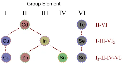
In the last ten years, numerous investigation at theoretical level, have been carried out in order to predict the formation mechanism and the physical properties of CZTSSe compounds. The formation of I2–II–IV–VI4 compounds like CZTSSe can be achieved from
an II–VI semiconductor by sequential replacement of cations in which the octet rule is respected and the total charge remains neutral (see Figure 12).
23
Figure 12: Formation of stoichiometric I2–II–IV–VI4 compounds can be achieved by a sequential replacement of
cations.
2.4.2.1 CZTSSe crystal structure
Binary compounds like CdTe adopt the cubic zincblende structure in which there are two interpenetrating face-centered cubic crystals [14]. The ternary I–III–VI2 semiconductor
alloys like CIS (in this case a chalcopyrite structure) can be built by replacing the group II atom with two atoms of group I and III [12-15]. Always respecting the octet rule, it is possible to split the ternary I–III–VI2 compound by replacing two atoms of group III with
two atoms respectively from group II and IV, forming a I2–II–IV–VI4 semiconductors.
Composition of quaternary compounds in a phase diagram can be rather complex to display. Since each element can in principle be varied independently of the others, we have to be very careful when using terms such as ‘Cu-poor’, ‘Zn-rich’ etc., which are commonly employed to describe CZTSSe films. These terms are intelligible when only one component varies, but when two or more components deviate from stoichiometry, the terminology can be misleading.
The fact that the chalcogens (S, Se) are not an independent variables, allows representing the alloy in a ternary phase diagram. In fact the amount of anions (chalcogens) introduced in the alloy depends on the amount of the cations and their valency: Cu(I), Sn(IV) and Zn(II). In the CZTSSe literature, the ratios of atomic percentages [Cu]/([Zn]+[Sn]) and [Zn]/[Sn] are often used to represent the composition of the cations in the alloy. Both ratios
24
are equal to one when the material is stoichiometric. However, these ratios are not independent, and therefore do not clearly show the deviations from stoichiometry in a particular case. A ternary phase diagram is the most useful way to summarize compositions in the Cu-Zn-Sn system. An example of a ternary phase diagram is shown in Figure 10.
Figure 13: Ternary composition diagram showing the position of stoichiometric CZTSSe [19].
The three sides of the plot each show the atomic percentage of one of the three metal elements. At any point in the diagram, the three values read off the axes will sum to unity. The circle in Figure 13 corresponds to the stoichiometric composition of CZTSSe compound.
A comprehensive analysis of the Cu2X-ZnX-SnX2 pseudo-ternary system (where X could
be S or Se) was carried out by Olekseyuk et al [19], who presented a phase diagram for the system at 400°C (Figure 14). Cu2ZnSnX4 as a single phase is present only within a rather
narrow range of compositions, which is indicated with an asterisk at the centre of the plot. In all other regions of the phase diagram there are up to two additional secondary phases present, always alongside CZTSSe.
25
Figure 14: Ternary phase diagram adapted from reference [19], showing the expected secondary phases at 400°C.
Taking the case of pure CZTS represented in Figure 11, there are five two-phase fields, in which one secondary phase will be observed in addition to CZTS. In between these there are five three-phase fields, where the secondary phase from both of the bordering regions will be formed alongside CZTS. Other phases not in this diagram but seen during the formation of CZTS in other reports include Cu4SnS6 and SnS2.

![Figure 28: Raman spectra of pure CZTS and CZTSSe with 90% selenium layers. Main peaks of CZTS and CZTSe [15] are reported](https://thumb-eu.123doks.com/thumbv2/123doknet/12872348.369381/74.918.276.686.562.895/figure-raman-spectra-cztsse-selenium-layers-cztse-reported.webp)