HAL Id: tel-00485723
https://tel.archives-ouvertes.fr/tel-00485723
Submitted on 21 May 2010
HAL is a multi-disciplinary open access archive for the deposit and dissemination of sci-entific research documents, whether they are pub-lished or not. The documents may come from
L’archive ouverte pluridisciplinaire HAL, est destinée au dépôt et à la diffusion de documents scientifiques de niveau recherche, publiés ou non, émanant des établissements d’enseignement et de
FOR MOLECULAR MEMORIES
Adrian Calborean
To cite this version:
Adrian Calborean. QUANTUM MODELING OF HYBRID SYSTEMS FOR MOLECULAR MEM-ORIES. Material chemistry. Université Joseph-Fourier - Grenoble I, 2009. English. �tel-00485723�
THESE
Pour obtenir le grade de
DOCTEUR DE L’UNIVERSITE JOSEPH FOURIER Discipline : CHIMIE PHYSIQUE
Présentée par
Adrian CALBOREAN
MODELISATION PAR LA CHIMIE QUANTIQUE DES
SYSTEMES HYBRIDES POUR DES MEMOIRES
MOLECULAIRE
Thése soutenue le 27 octobre 2009
Composition du jury Composition du juryComposition du jury Composition du jury
Prof. Carlo ADAMO Ecole Normale Supérieure Chimie Paris Rapporteur Dr. Dominique VUILLAUME CNRS – IEMN Rapporteur Prof. Anne MILET Université Joseph Fourier Examinateur Prof. Vasile CHIS Babes-Bolyai University Examinateur Dr. Pascale MALDIVI CEA Grenoble Directeur de thèse Dr. Philippe BLAISE CEA Grenoble Co-directeur de thèse
Service de Chimie Inorganique et Biologique Institut Nanosciences et Cryogénie, CEA Grenoble, France
École Doctorale Chimie et Sciences du Vivant
THESIS
For obtaining the degree of
DOCTOR OF THE JOSEPH FOURIER UNIVERSITY Specialty: PHYSICAL CHEMISTRY
Presented by
Adrian CALBOREAN
QUANTUM MODELING OF HYBRID SYSTEMS FOR
MOLECULAR MEMORIES
Thesis defended on 28 April 2009
Composition Composition Composition
Composition ofofof juryofjuryjuryjury
Prof. Carlo ADAMO Ecole Normale Supérieure Chimie Paris Rapporteur Dr. Dominique VUILLAUME CNRS – IEMN Rapporteur Prof. Anne MILET Université Joseph Fourier Examinator Prof. Vasile CHIS Babes-Bolyai University Examinator Dr. Pascale MALDIVI CEA Grenoble Thesis director Dr. Philippe BLAISE CEA Grenoble Thesis co-director
Service de Chimie Inorganique et Biologique Institut Nanosciences et Cryogénie, CEA Grenoble, France
Ce travail a été réalisé dans le cadre général du développement de nouveaux composants mémoires utilisant le stockage de charges grâce à des molécules rédox. Une collaboration combinant recherche fondamentale, dans notre laboratoire, et recherche appliquée avec des équipes du CEA/LETI a conduit à la conception de systèmes hybrides constitués d’une monocouche de molécules rédox greffées sur la surface de silicium, les différents états de charge des molécules servant à stocker l’information. Notre but était de comprendre les paramètres (molécule, lien) gouvernant les transferts de charge et les propriétés électriques de tels systèmes. L’objectif principal de la thèse a donc été de modéliser les propriétés électroniques de molécules rédox et des systèmes résultants de leur greffage sur Si, à l’aide de méthodes basées sur la Théorie de la Fonctionnelle de la Densité. Un premier volet a été consacré à l’étude de processus rédox dans des porphyrine métallées intéressantes pour leur bistabilité. Un deuxième volet rassemble toutes les études sur les systèmes de molécules rédox greffées sur Si. En raison de leur nature hybride, deux approches ont été utilisées. La première, basée sur une description moléculaire où la surface de Si est modélisée par un aggrégat, conduit à des données importantes telles que le gap HOMO-LUMO, la localisation des charges ou les propriétés structurales. La deuxième basée sur des calculs de système périodique où la surface de Si est infinie, donne accès aux densités d’états. Ces données ont été ensuite comparées aux calculs moléculaires et discutées en liaison avec les propriétés électriques déterminées sur des composants tests.
Mots MotsMots Mots----clésclésclés clés mémoires moléculaire, molécules rédox, porphyrine métallées, bistabilité, ferrocene, systèmes hybrides, Théorie de la Fonctionnelle de la Densité, système périodique.
Disc DiscDisc Disciplineiplineipline ipline Chimie physique moléculaire et structurale
Laboratoire LaboratoireLaboratoire Laboratoire Laboratoire de Reconnaissance Ionique et Chimie de Coordination Service de Chimie Inorganique et Biologique, UMR-E3 CEA-UJF Institut Nanosciences et Cryogénie, CEA Grenoble 17 Rue des Martyrs, 38054 Grenoble Cedex, France
Abstract
The general context of this work is the development of new electronic devices that utilize charge storage properties of redox-active molecules for memory applications. A collaborative approach involving both fundamental research in our laboratory and applied research teams from the CEA/LETI has lead to the design of hybrid systems for molecular memories. Monolayers of redox-active molecules are formed on the semiconductor Si surface and the stable charged states of the molecules are utilized to store information. Our purpose was to understand the main parameters (molecule, linker) which govern the charge transfer between semiconducting Si surface and redox molecules and the electrical behaviour of such systems.
The main objective of this thesis has thus been to develop Density Functional Theory approaches to describe the electronic properties of redox-active molecules and hybrid systems for the purpose of information storage. The first axis was dedicated to the modeling of redox processes of molecules such as metalloporphyrins with bistability properties. The second part was devoted to the study of redox-active molecules grafted on Si surface. Due to the hybrid nature of the latter systems, two approaches were developed. One was based on a molecular description, using Si aggregates in place of a Si surface, yielding a molecular orbital description of some relevant features: Homo-Lumo gaps, charge localization or structural properties. The other approach was focused on periodical calculations, with molecules grafted on ‘infinite’ Si surface. The resulting DOS were compared to molecular results, and discussed in the light of experimental data on electrical properties.
Keyword Keyword Keyword Keywordssss molecular memories, redox molecules, metallic porphyrin, bistability, ferrocene, hybrid systems, Density Functional Theory, periodical systems.
Specialty Specialty Specialty Specialty Molecular and structurale physical chemistry
Laboratory LaboratoryLaboratory Laboratory Laboratoire de Reconnaissance Ionique et Chimie de Coordination Service de Chimie Inorganique et Biologique, UMR-E3 CEA-UJF Institut Nanosciences et Cryogénie, CEA Grenoble 17 Rue des Martyrs, 38054 Grenoble Cedex, France
Acknowledgements
First and foremost, I would like to express my sincere appreciation to my advisor, Dr. Pascale Maldivi for her invaluable support, encouragement and guidance for the successful completion of my thesis.
I would also like to thank Dr. Philippe Blaise as thesis co-director, whose help and support during these three years were essential to me. I really appreciated his valuable advices and cordiality.
I would like to express my gratitude to Professor Carlo Adamo, Dr. Dominique Vuillaume Professor Anne Milet and Professor Vasile Chis for accepting to judge the quality of my work.
Particular thanks are addressed to Tiziana Pro, Julien Buckley, Florence Duclairoir and Lionel Dubois which brought a fundamental contribution to this work and have been patience and perseverance to discuss and work day after day.
I would like to acknowledge to Valentina Vetere, my office colleague, for her help and disponibility during the preparation of the thesis manuscript and the public defense. Also for the pleasant atmosphere that was in our office.
I would also like to thank Zohra Termache, the secretary the most effective I have encountered, for his availability and assistance.
Many thanks to former and present collaborators at the RICC Laboratory for their practical help, friendly support and encouragement during these years. Last but not least, I would like to thank my family and friends for their long-lasting patience and support.
The European Community through the Marie Curie CHEMtronics programme (MEST-CT-2005-020513) is deeply acknowledged for financial support.
Résumé étendu en français
En raison de l’augmentation constante de la densité des dispositifs à base de silicium, des limites physiques (effets quantiques et comportement non déterministe des faibles courants) et technologiques (comme la dissipation de la puissance, la complexité du design et l’effet tunnel des courants) peuvent intervenir et bloquer les possibilités de futur progrès de la microélectronique. Pour ces raisons, il est admis que la loi de Moore n’est plus valable ou que les lois d’échelle du CMOS sont désormais obsolètes.
L’électronique moléculaire a pour ambition de remplacer les technologies actuelles par des systèmes comportant une ou plusieurs molécules qui peuvent être utilisées comme interrupteurs, connections ou comme dispositifs logiques ou comme mémoires. L’approche aussi dit « bottom-up » consiste à créer des éléments fonctionnels à partir des plus petits éléments de construction, les molécules, avec l’opportunité supplémentaire d’obtenir un ordre structural à plus large échelle comme pour les transistors.
Les recommandations actuelles pour le développement des mémoires « flash » non-volatiles peuvent être résumées en deux voies distinctes. D’un coté il s’agit de rechercher de nouveaux matériaux et des nouvelles architectures de transistors afin de réduire les dimensions des dispositifs actuels. D’un autre coté, la recherche de nouvelles technologies s’appuie sur une électronique à l’échelle de la molécule ou de l’atome. Ces dernières technologies sont essentiellement fondées sur des mémoires moléculaires, qui peuvent être des dispositifs capacitifs (comme les mémoires Flash ou DRAM) ou des mémoires interrupteurs résistives qui utilisent une architecture dite « crossbar ». Dans ce projet, nous nous sommes intéressés au développement d’un dispositif capacitif hybride moléculaire qui utilise des molécules rédox comme composants actifs de stockage de charge.
Ces dernières années, beaucoup d’efforts ont été focalisés vers de nouveaux dispositifs de mémoires qui utilisent une approche hybride molecule/silicium et qui tiennent compte de l’incorporation de molécules organiques à des semi-conducteurs de Si. Ces types de
technologies actuelles.
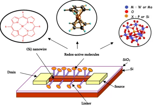
Dans ce cadre, nous avons décidé d’étudier des monocouches de molécules redox-actives liées a une surfaces de Si. Différents états stables de charge sont donc utilisés pour le stockage de l’information. Afin de mieux comprendre le design des systèmes moléculaires hybrides, le processus de l’opération écriture/effacement des mémoires flash est décrit figure.1.
Figure 1. Schéma d’écriture/effacement des mémoires FLASH
Le dispositif de mémoire à grille flottante (figure.1) stocke les informations en gardant la charge électrique dans la grille flottante. Si on ajoute ou on éloigne une charge de la grille
Writing/Erasing Operation Erasing
Writing SiO2 SiO2 Si Si Si
Les 2 états sont définis par la présence/l’absence des
électrons dans la grille flottante (FG)
Les charges dans la grille flottante induisent un
Si
RedoxRedoxRedoxRedox----active moleculesactive moleculesactive molecules active molecules
(Si) nanowireSi) nanowireSi) nanowireSi) nanowire
SiO2 Drain Drain Drain Drain Source Source Source Source Linker Linker Linker Linker
supérieure. Les 2 cas correspondent à deux états, 0 ou 1, et ils définissent si la cellule mémoire a été programmée ou effacée.
Nos systèmes de mémoires hybrides ont été inspirés par ces dispositifs et sont représentés en figure 2. Pour ce système, la couche redox-active joue le rôle de grille flottante. En appliquant un voltage qui correspond à un processus redox de la molécule, on devrait pouvoir transférer des électrons entre la molécule et le fil de Si. En général, une couche moléculaire permettant le stockage est constituée par un groupement rédox actif et un lien immobilisant de façon covalente la molécule à une surface semiconductrice.
Dans notre projet, nous avons choisi des molécules redox qui peuvent exhiber un ou plusieurs états redox distincts, comme le ferrocene, les porphyrines et les polyoxometallates (voir figure 2 pour des exemples).
Figure 2. Représentation schématique de mémoires moléculaires hybrides/Si.
L’objectif général du projet CEA (INAC et Leti) sur les mémoires moléculaires est donc la compréhension (expérimentale et théorique) des mécanismes qui régulent l’échange d’électrons entre le semi-conducteur Si et la molécule redox.
1) La première partie a été dédiée à la modélisation des molécules isolées qui montrent une bistabilité redox, comme les dérivées du ferrocene ou plusieurs porphyrines métalliques. La présence d’une bistabilité redox est une condition nécessaire afin de concevoir des dispositifs capables de stabiliser un état de charge sur un intervalle important de potentiel électrique. Des études préliminaires ont montré que des changements conformationnels pourraient induire ce type de bistabilité.
2) La deuxième partie est dédiée à l’étude de molécules redox greffées sur la surface de
Si. L’idée est donc de reproduire et interpréter grâce au méthodes théoriques l’influence de différents paramètres (molécule, métal central, lien covalent) sur les propriétés électriques (localisation de la charge, potentiel redox, caractéristique du dispositif).
Pour les molécules greffés sur la surface de Si (1 0 0), et en raison de la nature hybride des systèmes à décrire, nous avons décidé de comparer deux approches théoriques différentes. D’un coté nous avons utilisé une description moléculaire pour l’ensemble. Dans ce cas la surface de Si a été modélisée comme un agrégat et des méthodes DFT moléculaires nous ont permis de décrire les écarts HOMO-LUMO, la localisation de la charge et les propriétés de liaison chimique. Néanmoins, si cette approche décrit bien la molécule, elle n’est pas très bien adaptée à la description de la surface infinie de Si. Pour cette raison, nous avons développé une étude basée sur la physique de l’état condensé et sur des calculs périodiques. Afin d’éviter des problèmes lié à la description du gap (confinement de
surface
)
, nous avons commencé cette étude par la reconstruction de la surface de Si.Ensuite, nous avons développé des simulations de molécules choisies greffées sur la surface infinie. Ces calculs nous ont permis de calculer la densité projetée d’états (PDOS). Enfin, nous avons comparé les résultats obtenus avec les données expérimentales.
• Modéliser et caractériser des molécules redox qui sont intéressantes pour des applications dans des dispositifs électroniques
• Analyser la stabilité de ces molécules liées (directement ou indirectement) de façon
covalent à la surface de Si
• Analyser et décrire les propriétés électroniques des systèmes hybrides molécules/Si
• Analyser l’influence du lien sur le phénomène de transfert de charge
• Proposer une méthode théorique efficace, en termes de ressources informatiques et
temps CPU, pour la description de ces systèmes.
• Déterminer des propriétés électriques de matériaux hybrides adaptées aux
dispositifs électroniques nano.
Ces objectifs sont donc de deux types, méthodologiques d’un coté, de compréhension chimique des systèmes hybrides de l’autre.
L’objectif à long terme serait d’utiliser les propriétés électroniques calculées pour développer des modèles de transport quantique et pour la simulation des mémoires moléculaires.
Chapitre I
Le premier chapitre décrit l’état de l’art dans le domaine des mémoires moléculaires en s’intéressant surtout aux mémoires de type DRAM et Flash. Plusieurs exemples de systèmes expérimentaux sont montrés. Le rôle important de la bistabilité rédox est également souligné, en se basant sur des exemples de la littérature. Dans ces exemples, nous décrivons les différents matériaux moléculaires utilisés, les procédés d’ancrage de ces systèmes sur le substrat, ainsi que les techniques expérimentales de caractérisation. Ce chapitre permet donc de situer le contexte général du travail de thèse.
Un rappel des bases des méthodes théoriques standard utilisées dans ce travail est donné dans ce chapitre. Les systèmes moléculaires hybrides que nous avons étudiés pendant la thèse ont nécessité l’utilisation de deux approches théoriques : la Théorie de la Fonctionnelle de la Densité (DFT) et le formalisme de la physique de l’état solide décrivant les systèmes périodiques.
Chapitre III
Modélisation des propriétés moléculaires pour le stockage d’information. Modélisation des propriétés moléculaires pour le stockage d’information. Modélisation des propriétés moléculaires pour le stockage d’information. Modélisation des propriétés moléculaires pour le stockage d’information.
Dans le but de rechercher de nouvelles molécules capables de stockage d’informations et qui utilisent des états de charge, il est nécessaire de se focaliser et étudier les propriétés suivantes :
• Les propriétés redox : états et potentiels redox stables
• Propriétés structurales
• Corrélation entre les propriétés redox et paramètres structuraux (pour la recherche
de molécules bistables)
Par conséquent, notre premier objectif était donc d’être capable de reproduire les propriétés moléculaires (comme par exemples les paramètres géométriques, et les comportements énergétiques). En effet, la compréhension du phénomène de bistabilité nécessite une bonne reproduction des propriétés structurales en fonction de paramètres moléculaires comme les groupes fonctionnels, la nature du centre métallique, et l’état redox de la molécule. Cette dernière partie est principalement dédiée à l’étude des porphyrines bridées développées dans notre laboratoire.
Cette partie du travail est organisée en quatre parties. En premier lieu, nous étudions des espèces moléculaires simples qui sont des précurseurs des systèmes hybrides plus
Figure 3. a) Structure du Ferrocene ; b) tetraphenylporphyrine de Zn (ZnTPP)
Ensuite, nous avons porté notre attention sur des porphyrines plus complexes, toujours précurseurs de stockage de charge. Nous avons inclus dans cette étude l’analyse conformationelle de porphyrines meso-substituées en fonction du groupe méso et de la nature du métal (figure 4).
Figure 4. Porphyrine issue du Perilaldehyde (gauche); Porphyrine du Myrtenal (droite).
Enfin, nous nous sommes concentrés sur les propriétés structurales obtenues sur des porphyrines bridées (notées MBCP-8) qui contiennent un métal non redox (fig 5, 6) et précurseurs d’un comportement bistable.
Figure 5. Structure de NiBCP-8
Figure 6. Structure de ZnBCP-8
Enfin, nous décrirons quelques résultats préliminaires obtenus sur les porphyrines de MnII ou III.
Chaque partie de cette étude est basée sur les données expérimentales disponibles et qui seront discuté en parallèle de notre analyse des résultats théoriques. Les calculs ont été réalisés par des méthodes de chimie quantique basées sur la DFT. Nous avons obtenu dans tous les cas un très bon accord avec les données expérimentales, qu’elles soient structurales ou thermodynamiques.
Chapitre IV
Modélisation des systèmes hybrides molécule Modélisation des systèmes hybrides molécule Modélisation des systèmes hybrides molécule
Modélisation des systèmes hybrides molécule –––– SiSiSi Si
Dans notre travail, la structure générique d’un système hybride consiste en un groupe redox actif (la molécule en elle-même), une molécule liante et la surface semi-conductrice. Afin de décrire et de comprendre le transfert d’électrons correspondant et de le corréler avec les données expérimentales, nous avons besoin d’étudier une des propriétés clef de la structure électronique : l’alignement et la position relative des orbitales frontières de la molécule relativement au gap du substrat silicium. Nous avons ainsi besoin de décrire correctement les facteurs d’origine moléculaire qui influe sur cet alignement, et de les corréler avec les données expérimentales.
La difficulté principale avec de tels systèmes est leur nature hybride, étant construits à partir de molécules qui sont essentiellement des espèces localisées qui interagissent avec un système infini. La méthode que nous choisirons pour décrire le gap de tels systèmes représente une option décisive. Cette difficulté a déjà été identifiée et discutée dans la littérature. Dans notre contexte, nous avons utilisé deux approches théoriques pour comparaison. L’une est basée sur une description moléculaire, en remplaçant la surface par un petit agrégat de silicium, conduisant à une approche en orbitales moléculaires des caractéristiques suivantes : gaps Homo-Lumo, localisation de la charge, propriétés structurelles (figure 7).
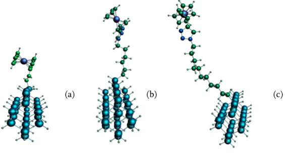
Figure 7. Structure géométrique de : (a) Ferrocene lié directement (b) Fc-N3(CH2)6, (c) Fc-N3(CH2)11 en liaison indirecte.
L’autre approche s’est concentrée sur des calculs de structures périodiques, avec des molécules accrochées sur une surface infinie (Figures 8 et 9). Les densités d’états issues de ces calculs ont été comparées avec les résultats moléculaires, et analysées à la lumière des résultats de mesures électriques.
L’approche utilisant la DFT moléculaire conduit à une description des niveaux HOMO et LUMO de la molécule et du Si qui permettent parfaitement de comprendre le comportement expérimental en terme de transfer de charge, même si le gap HOMO-LUMO est trop grand. Les calculs périodiques montrent que globalement l’ordre des niveaux moléculaires est le même que dans les calculs DFT standard, et qu’il n’y a aucun couplage avec les états du silicium.
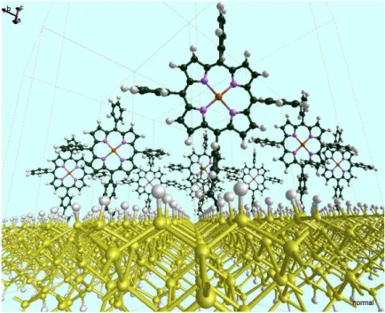
Figure 9. Structure optimisée de ZnTPP en liaison directe sur SI (1 0 0)
Chapitre V
La stabilité et la résistance des molécules organiques envisagées sont cruciales pour transposer cette technologie depuis la recherche jusqu’au développement et à la production. Les ferrocènes et les porphyrines sont des molécules d’une grande stabilité à température ambiante dans des conditions standard. Cependant, lorsqu’ils sont immobilisés sur une surface de Si, ce qui est important est la stabilité et le comportement
quantique à partir du ferrocène greffé, à l’état neutre et oxydé.
Les deux systèmes présentent une stabilité thermique à température ambiante à une échelle de temps court. Bien que préliminaires, ces résultats montrent en particulier que la molécule ne se dépose pas sur la surface de silicium. Des atomes d’hydrogène semblent réagir en premier, et nous attendons qu’une augmentation de température entraine une désorption de l’hydrogène de la surface, comme cela est bien connu en microélectronique, pour des températures entre 600 et 1300K. Ces calculs sont très lourds et ces premiers résultats devraient donc être poursuivis avec des systèmes avec les espaceurs plus longs ainsi que avec les porphyrines.
Résultats Principaux et conclusionsRésultats Principaux et conclusionsRésultats Principaux et conclusions Résultats Principaux et conclusions
Dans la première partie, sur les propriétés moléculaires des dérivés de ferrocène et de métallo-porphyrines, nous avons montré que les calculs en DFT standard des potentiels redox sont en bon accord avec les mesures expérimentales à condition de tenir compte correctement du solvant (via la méthode PCM), et bien que nous négligions certains paramètres thermodynamiques comme l’énergie de point zéro (ZPE) et les variations d’entropie. Nous avons reproduit également de façon remarquable l’ensemble des propriétés structurales de complexes de Zn et Ni à partir de porphyrines bridées, y compris dans différents solvants. Pour autant, les porphyrines à base de manganèse (II) nécessitent de pousser plus loin notre étude, car la description correcte de leur structure électronique reste un défi pour la DFT, sachant que grâce à l’approche ab initio de type CAS nous devrions être capable de résoudre ce point.
La deuxième partie, dédiée à la description des molécules greffées sur une surface de silicium, a donc été réalisée en deux volets. La première méthode utilisée décrit la surface
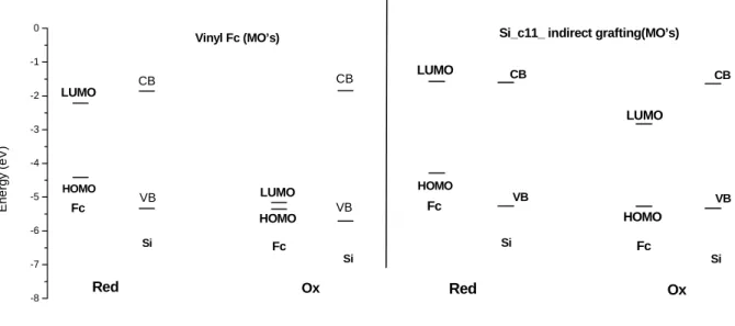
précis et permet de traiter un environnement tel que le solvant. La contrepartie est un gap du silicium faux, avec une énergie trop élevée pour le niveau Lumo (bas de la bande de conduction du silicium). Néanmoins, l’augmentation de la taille du cluster permet de décroitre le gap en faisant baisser le niveau Lumo. A vrai dire, les niveaux Homo et de la bande de valence du silicium sont très proches de ceux obtenus avec un calcul périodique. Nous avons aussi obtenus en calculs moléculaires, de bons potentiels redox (comparés aux mesures expérimentales). Nous avons observé également une forte localisation de la charge sur les molécules greffées. De plus nous avons pu quantifier certaines différences dans l’alignement des gaps (molécule et surface de Si) en fonction du type de greffage (direct ou indirect), qui sont bien corrélées aux données expérimentales de voltammétrie cyclique. Par exemple, les résultats d’alignements des niveaux moléculaires et du gap du Si sont représentés pour le ferrocène figure 10.
Figure 10. Comparison de l’alignement des niveaux HOMO-LUMO et gap Si. Gauche: lien direct; droite: lien indirect (C11).
La figure 10 (gauche) montre que les gaps HOMO-VB pour l’espèce réduite et LUMO-VB de l’espèce oxydée sont très proches en énergie. Cela est cohérent avec des valeurs
similaires de potentiel d’oxydation et de réduction (Vox≈Vred). Ceci est en accord avec la
-8 -7 -6 -5 -4 -3 -2 -1 0 CB CB VB Si Si Fc Fc LUMO LUMO HOMO HOMO Ox Vinyl Fc (MO’s) E n e rg y ( e V ) Red VB CB CB VB VB Si Si Fc Fc LUMO LUMO HOMO HOMO Ox
Si_c11_ indirect grafting(MO’s)
Pour le greffage indirect, avec Fc-N3(CH2)6 et Fc-N3(CH2)11, le transfert électronique n’est
pas réversible au même potentiel et |Vox|>|Vred|. Ceci corrobore les voltammétries cycliques où on observe un écart plus important entre les potentiels d’oxydation et de réduction. Ainsi, ces modèles semblent bien reproduire les données expérimentales et permettent de mettre en évidence des corrélations entre les calculs moléculaires, et l’électrochimie ainsi que les mesures de capacitance. Des résultats analogues ont été trouvés pour les porphyrines de Zn greffées par un lien direct ou indirect.
La seconde méthode, par des calculs périodiques, est a priori moins précise dans la description des niveaux moléculaires et n’est pas capable d’évaluer les potentiels redox, mais elle permet d’obtenir une meilleure description de l’alignement des niveaux d’énergie. Sur la figure 11 est représenté un exemple de PDOS calculé sur une espèce Fc greffée de façon directe.
Nous retrouvons un alignement des gaps proche de ce qui était obtenu en calculs moléculaires. Ainsi cela permet de calibrer les calculs moléculaires et d’identifier les problèmes dus à la mauvaise description du gap. Dans notre cas, les deux méthodes (moléculaire et périodique) donnent les mêmes résultats concernant les différentes énergies mises en jeu dans le transfert d’électron dû aux processus d’oxydation et de réduction. Cela est principalement dû au fait que nous n’avons pas besoin de prendre en compte la bande de conduction, dont la position est pourtant clairement incorrecte en description moléculaire. En effet, dans les expériences, le Si est dopé p, donc tous les transferts électroniques ont lieu avec la bande de valence (VB). Aussi, un autre effet sous-jacent, qui a certainement joué en notre faveur est que les différents groupes de niveaux d’énergie (molécule, lien covalent, Si) ne sont pas en interaction mutuelle ou en tous cas pas directement couplés. Ainsi, nous pouvons décrire le système total comme une superposition de deux sous-systèmes, la molécule et la surface de silicium, faiblement couplés. En réalité, un dipôle électrostatique d’interface d’origine moléculaire a pu être identifié.
Finalement, connaissant les avantages et inconvénients de chaque méthode, les conclusions de cette partie nous permettront de définir à l‘avenir des simulations plus efficaces de tels systèmes hybrides. Ainsi d’autres systèmes hybrides pourront être étudiés par exemple en impliquant d’autres types de transferts de charge. Et pour aller plus loin, les propriétés de transports pourraient être évaluées en partant de nos résultats de calculs ab initio qui serviraient de données d’entrée pour des calculs de transport quantique.
Table of contents
Résumé Résumé Résumé Résumé vvvv Abstract Abstract AbstractAbstract viiviiviivii
Acknowledgements Acknowledgements Acknowledgements Acknowledgements ixix ixix Table of contents Table of contents Table of contents
Table of contents xxviixxviixxviixxvii
IntroductionIntroductionIntroductionIntroduction
1111.1. .1. .1. Overview of Hybrid Elec.1. Overview of Hybrid ElecOverview of Hybrid ElectronicOverview of Hybrid Electronictronictronic 1
1.1.1. CMOS scaling: Challenges and Strategies 2
1.1.2. Molecular electronics technology for further electronic applications 6
1.1.3. Emerging Molecular memories 7
1111.2. Molecular Memories project.2. Molecular Memories project.2. Molecular Memories project .2. Molecular Memories project 10
1.2.1. General framework 10
1.2.2. Theoretical approach and objectives 13
I.3. P I.3. P I.3. P
I.3. Presentation of work resentation of work resentation of work resentation of work 16
Chapter I Chapter I Chapter I
Chapter I State of the art State of the art State of the art –––– Molecular memories: literature, laboratory investigations State of the art Molecular memories: literature, laboratory investigations Molecular memories: literature, laboratory investigations Molecular memories: literature, laboratory investigations 22222222 IIII.1..1..1..1. Current Memory devicesCurrent Memory devicesCurrent Memory devicesCurrent Memory devices 22
I.1.1. Volatile vs Non-Volatile memories 22
I.1.2. Non-Volatile Flash memory 24
IIII.2..2..2..2. The future of NonThe future of NonThe future of NonThe future of Non----Volatile MemoriesVolatile MemoriesVolatile MemoriesVolatile Memories 25
I.2.1. Non-Volatile memories based on inorganic materials 26
I.2.2. Organic memories using bulk switching effects 27
I.2.3. Molecular memory. Emerging routes 29
I.2.3.1. Resistive switching memories 29
I.2.3.2. Capacitive Molecular memories 39
1.2.3.3. Floating Gate memories 43 I.3
I.3 I.3
I.3. . . . Molecular memories and bistable moleculesMolecular memories and bistable moleculesMolecular memories and bistable moleculesMolecular memories and bistable molecules 47
I.3.1. Bistable Porphyrins at CEA 53
IIII.4. .4. .4. .4. Molecular Molecular Molecular Molecular materials, materials, Atachment methods, Characterization tehniquesmaterials, materials, Atachment methods, Characterization tehniquesAtachment methods, Characterization tehniques Atachment methods, Characterization tehniques 55 1.4.1
1.4.1 1.4.1
1.4.1. . . . Molecular Materials and PropertiesMolecular Materials and PropertiesMolecular Materials and PropertiesMolecular Materials and Properties 55
1.4.1.1. Ferrocene molecule 55 1.4.1.2. Porphyrin family 56 1.4.2 Attachment methods 1.4.2 Attachment methods 1.4.2 Attachment methods 1.4.2 Attachment methods 59
1.4.3.2. Atomic Force Microscopy 62
1.4.3.3. Cyclic Voltammetry 64
1.4.4. Capacitance-Voltage and Conductance -Voltage characterization 66
1.4.5.Electrical model 68
Chapter II Theory and Methodology Chapter II Theory and Methodology Chapter II Theory and Methodology
Chapter II Theory and Methodology 81 818181 Introduction 81 II.1
II.1 II.1
II.1. . . . HartreeHartreeHartree----Fock THartree Fock TFock TFock Theoryheoryheoryheory 83
II.1.1. The variational principle 83
II.1.2. Hartree-Fock approximation. Slater determinant 84
II.1.3. Energy expression 85
II.1.4. Hartree-Fock equations 86
II.1.5. Restricted and Unrestricted Hartree-Fock models 88
II.1.6. The Roothan-Hall equations 89
II.1.7. Electron Correlation 90
II.1.7.1. Møller-Plesset Perturbation Theory 91
II.1.7.2. Configuration Interaction 92
II.1.7.3. Multi-Configurational Self Consistent Field 94
II.1.7.4. Coupled Cluster 95
II.2 II.2 II.2
II.2. . . . DensDensDensDensity Functional Theory ity Functional Theory ity Functional Theory ity Functional Theory 97
Introduction 97
II II II
II.2..2..2..2.1. Hohenberg 1. Hohenberg 1. Hohenberg 1. Hohenberg ––––Kohn theoryKohn theoryKohn theory Kohn theory 98
II.2.1.1. The first theorem 98
II.2.1.2.The second theorem 98
II.2.2 II.2.2 II.2.2
II.2.2. . . . KohnKohnKohn----Sham approachKohn Sham approachSham approach Sham approach 99
II.2.2.1 Kohn-Sham equations 101
II.2.3 II.2.3 II.2.3
II.2.3. . . . ExchangeExchangeExchange----correlation functionals Exchange correlation functionals correlation functionals correlation functionals 103
II.2.3.1. Local Density Approximation 104
II.2.3.2. Generalized Gradient Approximation 105
II.2.3.3. Hybrid Functionals 106
II.2.3.3.1 The Adiabatic Connection 107
II.2.4. Basis set II.2.4. Basis set II.2.4. Basis set
II.2.4. Basis set 109
II.3 II.3 II.3
II.3.... Solid State Physics Theory of Semiconductors Solid State Physics Theory of Semiconductors Solid State Physics Theory of Semiconductors Solid State Physics Theory of Semiconductors 114
II.3.1. Periodic systems and Bloch theorem 114
II.3.1.1. Periodic boundary condition 114
II.3.1.2. Born von Kárman periodic boundary condition 115
II.3.1.3. Bloch's theorem and Bloch waves 116
II.3.2 II.3.2 II.3.2
II.3.2. . . . The pseudopotential or effective potential The pseudopotential or effective potential The pseudopotential or effective potential The pseudopotential or effective potential 118
II.4.1. Verlet Algorithm 122
II.4.2. Thermalization of the system 123
II.4.3. Annealing method 124
II.5. Computational softwares II.5. Computational softwares II.5. Computational softwares
II.5. Computational softwares 124
II.5.1. Amsterdam Density Functional 125
II.5.2. Siesta 126 Chapter III Modeling of molecular properties for information storage
Chapter III Modeling of molecular properties for information storage Chapter III Modeling of molecular properties for information storage
Chapter III Modeling of molecular properties for information storage 132132132132
Introduction 132
IIIIII.1. Computational studies of simple redox molecular species II.1. Computational studies of simple redox molecular species II.1. Computational studies of simple redox molecular species II.1. Computational studies of simple redox molecular species 133
III.1.1. Theoretical approach 133
III.1.2. Ferrocene species 134
III.1.3. Zn porphyrins 137
III.2 III.2 III.2
III.2.... Computational studies of chiral meso-(α,β-unsaturated)-porphyrins 140
III.2.1. Main experimental structural features 141
III.2.2. Theoretical study 142
III.3. Bridled porphyrins: towards possible bistable complexes III.3. Bridled porphyrins: towards possible bistable complexes III.3. Bridled porphyrins: towards possible bistable complexes
III.3. Bridled porphyrins: towards possible bistable complexes 150
III.3.1. Experimental characterization III.3.1. Experimental characterization III.3.1. Experimental characterization
III.3.1. Experimental characterization 150
III.3.1.1. Solid state behaviour 150
III.3.1.2. Solution behaviour 152
III. III. III.
III.3.2. Theoretical study3.2. Theoretical study3.2. Theoretical study3.2. Theoretical study 153
III.3.2.1. Computation of ZnBCP-8 and NiBCP-8 153
III.3.2.2. Formation of dimers 157
III.3.2.3. Estimation of thermodynamic parameters for the open/closed
equilibriums in MBCP-8 162
IIIIIIIIIIII.4.4.4. Mn (II) and Mn (III) por.4. Mn (II) and Mn (III) por. Mn (II) and Mn (III) porp. Mn (II) and Mn (III) porppphyrins hyrins hyrins hyrins 164 IIIIII.4II.4II.4II.4.1..1..1. Computation of spin states ordering in Mn(II) and (III) porphyrins.1. Computation of spin states ordering in Mn(II) and (III) porphyrinsComputation of spin states ordering in Mn(II) and (III) porphyrinsComputation of spin states ordering in Mn(II) and (III) porphyrins 165
II.4.1.1. Literature data on simple Mn porphyrins 165
III.4.1.2. Theoretical study on simple Mn porphyrins 166
III.4 III.4 III.4
III.4.2..2..2. Bridled Mn porphyrins .2.Bridled Mn porphyrins Bridled Mn porphyrins Bridled Mn porphyrins 170
III.4.2.1. Literature data on bridled Mn porphyrins 170
III.4.2.2. Computations of bridled Mn porphyrins 171
Conclusions 174
Chapter IV Modeling Chapter IV Modeling Chapter IV Modeling
Chapter IV Modeling of hybridof hybridof hybrid molecule of hybridmolecule molecule molecule ----Si systems Si systems Si systems Si systems 179
Introduction 179
IV.1. Si surface 180
IV.1.1.Some general concepts 180
IV.1.2. Modeling of Si molecular approach 183
IV.1.3. Periodical calculations of Si (1 0 0) 186
IV.2. Ferrocene grafted on Si IV.2. Ferrocene grafted on Si IV.2. Ferrocene grafted on Si
IV.2. Ferrocene grafted on Si 189
IV.2.2.2 Indirect grafting 198
IV.2.2.2.1 The case of Fc-N3(CH2)6 indirect grafting 198
IV.2.2.2.1 The case of Fc-N3(CH2)11 indirect grafting 200
IV.2.2.3 Linker effect 201
IV.3. Periodical calculations on ferrocene grafted IV.3. Periodical calculations on ferrocene grafted IV.3. Periodical calculations on ferrocene grafted
IV.3. Periodical calculations on ferrocene grafted 204
IV.3.1. Density of States 204
IV.3.2. PDOS of directly grafted FcV.3.2. PDOS of directly grafted FcV.3.2. PDOS of directly grafted Fc----SiV.3.2. PDOS of directly grafted Fc SiSiSi 205
IV.3.2.1. PDOS of Fc-Si 205
IV.3.2.2. Comparison with quantum molecular results 208
IV.3.3. PDOS of indirect grafting of Fc on Si IV.3.3. PDOS of indirect grafting of Fc on Si IV.3.3. PDOS of indirect grafting of Fc on Si
IV.3.3. PDOS of indirect grafting of Fc on Si 209
IV.3.3.1. The case of Fc-N3(CH2)6 indirect grafting 204
IV.3.2.1. The case of Fc-N3(CH2)11 indirect grafting 211
IV.3.2.2. Comparison of PDOS between direct grafting and long chains 214 IV.4. Theoretical modeling of porphyirins grafted on Si (1 0 0)
IV.4. Theoretical modeling of porphyirins grafted on Si (1 0 0) IV.4. Theoretical modeling of porphyirins grafted on Si (1 0 0)
IV.4. Theoretical modeling of porphyirins grafted on Si (1 0 0) 214
IV.4.1. Main experimental structural features 215
IV.4.2. Theoretical molecular study of porphyrin grafted on Si IV.4.2. Theoretical molecular study of porphyrin grafted on Si IV.4.2. Theoretical molecular study of porphyrin grafted on Si IV.4.2. Theoretical molecular study of porphyrin grafted on Si 220
IV.4.2.1. Direct grafting of ZnTPP 217
IV.4.2.2. Indirect grafting of ZnTPP 220
IV.4.2.2.1. The case of ZnTPP- N3(CH2)6 220
IV.4.2.2.2 The case of ZnTPP- N3(CH2)11 221
IV.4 IV.4 IV.4
IV.4....3333. . . . PerioPerioPeriodical calculations on poprhyrin graftedPeriodical calculations on poprhyrin grafteddical calculations on poprhyrin grafted dical calculations on poprhyrin grafted 223
IV.4.3.1. PDOS of directly grafted ZnTPP 223
IV.4.3.2. Comparison with molecular computation 226
IV.4. IV.4. IV.4.
IV.4.3333....3. PDOS for indirect grafting of ZnTPP3. PDOS for indirect grafting of ZnTPP3. PDOS for indirect grafting of ZnTPP3. PDOS for indirect grafting of ZnTPP 227
IV.4.3.3.1.The case of ZnTPP- N3(CH2)6 227
IV.4.3.3.2. The case of ZnTPP- N3(CH2)11 229
IV.4.3.3.3. Comparison with molecular computation 232
IIIIV.5V.5V.5. CoV.5. Co. Co. Conclusionsnclusionsnclusionsnclusions 232
Chapter V Molecular Dynamics Chapter V Molecular Dynamics Chapter V Molecular Dynamics
Chapter V Molecular Dynamics 237
V.1. Main experimental structural features 237
V.2. Theoretical study 238
V.2.1. Theoretical method 238
V.2.2. Main results on ferrocene grafted 239
V.2.3. General trends 241
Conclusions Conclusions Conclusions
Introduction
1.1. Overview of Hybrid electronics
The beginning of molecular electronics is generally believed to have occurred in 1974
when Aviram and Ratner [1] have proposed a model that was probably the first
comprehensive theoretical example of unimolecular quantum transport. In particular, they have been inspired by the first studies on charge and energy transfer in molecules of Robert Mulliken and Albert Szent-Gyorgyi in the 1940’s, on the so-called donor-acceptor systems [2]. Charge transfer was made tangible by the proposal of Aviram and Ratner to use a Mulliken-like electron donor-acceptor molecule, separated by a sigma-bonded tunnelling bridge. They theoretically calculated and demonstrated that the current-voltage characteristics of such a system behaved like a rectifying diode similar to a semiconductor p-n junction [1]. Their work was pioneering thanks to their first considerations of using single molecules as the active elements in hybrid electronic structures.
Nowadays, molecular electronics is envisioned as a promising candidate for the nanoelectronics of the future. More than a possible answer to the ultimate miniaturization problem in nanoelectronics, molecular electronics is foreseen as a possible and reasonable way to assemble a large numbers of nanoscale objects (molecules, nanoparticles, nanotubes and nanowires) to form new devices and circuit architectures.
1.1.1. CMOS scaling: Challenges and Strategies
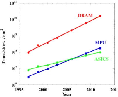
According to Intel co-founder Gordon Moore, the number of transistors per square centimeter of silicon doubles every 18 to 24 months [3]. This performance increase has been obtained mainly by decreasing the size of circuit dimensions obtained by optimization and improvement of existing technology. If plotted on a logarithmic scale (figure 0.1), the decrease in size of micro-electronic components versus the year gives a straight line. In few decades to come, the dimensions of the components should approach the size of about one nanometer.
Figure 0.1. Plot of transistor densities against dates of introduction [4]. The curve shows counts doubling every two years.
With the continuous increase in the density of silicon-based devices, the process scaling in semiconductor technology will soon reach physical and technical limits. Other concerns, such as gate oxide thickness, power consumption, and fabrication costs, also highlight the difficulty of scaling standard electronics materials to molecular dimensions [5].
In this context, there is thus a revival of efforts to build devices with molecular-scale components. At device areas of a few tens of square nanometers, molecules have an inherent attractiveness because: 1) of their size; 2) they represent the ultimate goal in terms of atomic control over physical properties; 3) of various properties that can be achieved through such control.
In this light, the semiconductor industry through the Semiconductor Industry Association (SIA) proposed a Microelectronics Roadmap on the future of CMOS (Complementary Metal Oxide Semiconductor) technology. They provided data predominantly on the scaling of dynamic random access memory (DRAM), microprocessing units (MPU) and applications specific integrated circuits (ASICs) manufacture. The major research and development inside the main semiconductor manufacturers is in line with the SIA roadmap predictions [6]. The roadmap predicts a steady reduction in the feature size (figure 0.2) combined with a steady rise in density (figure 0.3) until the year 2012.
The minimum feature size is fast approaching 10 nm in the next decade with switching charges containing 1000 or less electrons. There are still a number of technological
challenges required to be solved if CMOS is to reach the 19 nm and 1010 transistors per cm2
in 2012 [6-9].
Figure 0.3. Number of transistors per cm2 plotted against the year of first manufacture
(green - application-specific integrated circuit ASICs, blue – microprocessor unit MPU, red - dynamic random access memory DRAM)
Physical limits (quantum effects and non-deterministic behaviour of small currents) and technological limits (such as power dissipation, design complexity and tunnelling currents) may hinder the further progress of microelectronics on the basis of conventional circuit scaling. They are frequently cited as the reason Moore’s Law is “broken”, or why CMOS scaling is coming to an end.
At this moment the industrial and academic communities are searching for solutions to meet these challenges with: (1) non-classical CMOS to extend the life of CMOS technology and (2) fundamentally new technologies which rely on electronics at the level of individual atoms and molecules.
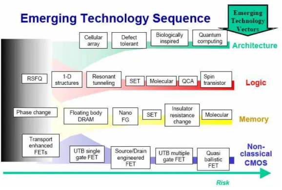
Several emerging technology vectors based on nanomaterials and nanostructures have been well identified by the International Technology Roadmap for Semiconductors (ITRS) [10]. Figure I.4 shows the ITRS emerging technology sequence for various technology
Figure 0.4 ITRS emerging technology sequence
There are six emerging research memory areas beyond traditional RAM and FLASH devices, that include phase change memory, floating body DRAM, nano floating gate memory, single electron memory, insulator resistance change memory, and molecular memory, which are also positively reviewed in [11 -13]:
• Phase Change Memory (PCM) [14], is a type of non-volatile computer memory
that uses the unique behaviour of chalcogenide glass, which can be "switched" between two states, crystalline and amorphous, with the application of heat. Recent versions can achieve two additional distinct states, effectively doubling its storage capacity. PCM can offer much higher performance in applications where writing quickly is important, both because the memory element can be switched more quickly, and also because single bits may be changed to either 1 or 0 without needing to first erase an entire block of cells.
• Floating body DRAM and nano-floating gate memory are the other technologies
which may come into the memory market in the next few years. The former is a one-transistor (1T) DRAM architecture, which stores data by charging the floating
body of the transistor, thereby enabling very high density [15-18]. The latter is a slight modification of conventional floating gate memory used in FLASH memory, where data is now stored in nanocrystals instead of a continuous film [19]. This can significantly improve the endurance and retention of the memory cells.
• A single electron tunnelling (SET) transistor device is a three terminal device based
on the Coulomb blockade. It consists of two tunnel junctions sharing one common electrode with a low self-capacitance, known as the island. The electrical potential of the island can be tuned by a third electrode (the gate), capacitively coupled to the island [20]. Although the current varies periodically with gate voltage, in contrast to the threshold behaviour of the field-effect transistor a SET could still form a compact and efficient memory device.
• Another approach to memory that is still in its early research stage is the Insulator
Resistance Change Memory [21], where a metal-insulator-metal structure is used. The change in (higher and lower) resistance states of the insulator occur under applied voltages. Owing to their very long retention time, these compounds are interesting candidates for non-volatile memory applications. The main challenge in this technology is in the development of new materials and integration.
• Molecular memory is a term for data storage technologies that use molecular
species as the data storage element, rather than circuits, magnetics, inorganic materials or physical shapes [22].
Although these new technologies that can be considered alternative to CMOS may not involve bulk Si, it would still be preferable for them to be compatible with CMOS, which has been the pole of the electronics industry for more than 30 years.
1.1.2. Molecular electronics technology for further electronic
applications
logic or memory devices [24-29]. Molecules are self -assembled into devices, thus creating conductive and strong interconnects.
In the conventional “top-down” approach used by microelectronics industry, silicon nanostructures are patterned in bulk materials by a combination of lithography, etching and deposition to form functional devices [30]. The “bottom-up” approach [31], on the other hand, implies the construction of functionality, electron storage, using small building units such as molecules, with the opportunity to have the molecules further self – assembled into the higher ordered structural units such as transistors. Self–assembly [32, 33] is a thermodynamically favourable process, where entities interact to form some organized aggregate structure. This approach could lead to enormous advances in future manufacturing for electronics [34].
Until now, miniaturization in electronics has been achieved by the top-down approach thanks to the improvement of the lithographic step. However, the current trend is not further sustainable using this strategy. Technological and economical limitations related to the growing difficulties in fabricating smaller and smaller devices complete this picture. Gaining the nanometer scale and/or further enhancing computational capabilities requires a turning point, a change in architecture and the development of conceptually new devices to overcome the physical and technological limitations of the top-down approach. In the following, we will focus on the emerging routes toward molecular memories, and in particular on the non-volatile memories.
1.1.3. Emerging Molecular Memories
In order to meet technology scaling in the field of solid-state memory and data storage, the mainstream transistor-based flash technologies will start evolving to incorporate material and structural innovations. In figure 0.5 are shown schematically the directions for the future developments of the non-volatile flash memories. Starting from the current technology, are proposed two distinct ways.
Figure 0.5 Emerging routes for non-volatile memories
The first one is pushing the scaling limits by developing new materials and new transistor structures, while the latter one is based on the development of new technologies, which rely on electronics at the level of individual atoms and molecules. These technologies are essentially based on molecular memories, that could be capacitive devices including Flash or DRAM –like approach or resistive switching memories using crossbar architectures. In this project, we are concentrating on developing hybrid molecular “capacitive devices” containing redox –molecules as the active component for charge-storage medium.
Hybrid silicon/molecular approach refer to the incorporation of organic molecules on the semiconductor Si platform to create a new class of memory devices. It has been the subject of a growing interest in the recent years as they offer possible options to overcome the current limitations (increasing processing costs, reliability, and variability) of standard silicon technology [35-40]. Some of the key advantages of this technology are listed
1. Easy integration with existing fabrication process - the number of additional steps involved in incorporating organic molecules on a silicon platform may be minimal. The size of molecules is between 1 and 100 nm, a scale that permits functional nanostructures with accompanying advantages in cost, efficiency, and power dissipation.
2. Assembly and recognition - molecular monolayers can be easily self-assembled on a variety of different substrates, including silicon, dielectrics and metal, by functionalizing them with appropriate linkers [41, 42]. Molecular recognition can be used to modify electronic behaviour, providing both switching and sensing capabilities on the single-molecule scale.
3. Synthetic tailorability of molecules – organic molecules with up to 8 multiple stable redox states have been already synthesized [43], and can provide multiple bits in a single memory cell. The latter possibility represents a significant advantage of molecular devices over conventional semiconductor and other memory technologies. Furthermore, the write/erase voltages and retention times can be tailored by varying for example the tethers attached to the end of the molecules or the spacers between the molecules and surface. By choice of composition and geometry, one can extensively vary transport, binding, optical, and structural properties of the molecules.
4. Dynamical behaviour: many molecules have multiple distinct stable geometric/ electronic structures, thus molecular switches between two stable structures can be obtained.
5. Discrete energy levels – the discrete nature of the MOs are preserved in a monolayer of molecules, resulting in discrete electronic states. Hence, the amount of charge stored will only depend on the number of molecules and not on the applied voltage.
6. Engineering the substrate and surface – the write/erase voltages and retention times can also be tuned. This can also lead to novel functionalities [44].
The main challenges in this field are:
1. Stability of molecules – organic molecules need to be stable at elevated temperatures
of at least 4000C in order to be able to integrate with the existing CMOS technology. The
4500C [45], so there are reasons to believe that this challenge can be overcome. The
stability of linkers that covalently bond molecules to substrates and the role of contaminants, are some other stability issues that need to be addressed.
2. Reliability and endurance under electrical stress – this is an unknown quantity in this field. Reported data have not yet established direct links between device behaviour and molecular properties. Until now, just the group of Bocian from University of California has demonstrated the molecular stability of the porphyrin molecules after millions of writing/erasing cycles [45].
3. Contact engineering – although there have been demonstrations of metal evaporation directly on molecules, it is still unclear whether the inherent molecular properties are retained after metal deposition.
4. Characterization techniques – there is need to identify efficient techniques or develop new techniques to characterize hybrid silicon-molecular devices.
Moreover, for the next memory device to be considered as a silver bullet solution it is necessary to possess the following attributes: 1) fast access time, 2) non-volatility, 3) infinite read/write cycles, 4) low power, and 5) a wide operating temperature range. From a manufacturing perspective, additional attributes are also required such as 6) scalability, 7) low cost, 8) manufacturability, 9) variability (of nanodevice feature size), and 10) integration ability with the Si platform.
In order to overcome all the challenges and to benefit of all the advantages that this field offers, it is essential to study, characterize and understand the physics of these devices.
1.2. Molecular Memories Project
1.2.1. General framework
Considering the aims and challenges above mentioned, one strategy has been developed in the last ten years to design electronic devices based on charge storage of
One such approach is developed in our project, where monolayers of redox-active molecules are formed on the semiconductor Si surface and the multiple stable charged states of the molecules are used to store information.
In order to better understand the design of such hybrid molecular devices, we show firstly
on figure 0.6the principle of writing/erasing operation in flash memories.
Figure 0.6. Writing/Erasing Scheme of FLASH memory
The floating gate memory device
(
figure 0.6, top)
stores information by holding electricalcharge within the floating gate. Adding or removing charge from the floating gate,
changes the threshold voltage VT of the cell between a low and a high value to represent
logic 0 and 1, respectively (figure 0.6, bottom), thereby defining whether the memory cell is in a programmed or erased state. Inspired from this design, molecular hybrid systems currently under investigation are represented on figure 0.7. In such a hybrid device, the redox-active monolayer plays the role of the floating gate. Application of a voltage corresponding to a redox process of the molecule should cause the redox-active monolayer
Writing/Erasing Operation Erasing
Writing SiO2 SiO2 Si Si Si Drain Current
The two states are defined by the presence/absence of electrons in the floating
gate (FG)
Charges in the floating gate induce a shift in VT
Si
RedoxRedoxRedox----active moleculesRedoxactive moleculesactive moleculesactive molecules
(Si) nanowireSi) nanowire Si) nanowireSi) nanowire
SiO2 Drain Drain Drain Drain Source Source Source Source Linker Linker Linker Linker
to transfer electrons between the molecule and the Si nanowire. Typically, a redox-active
compound consists of a charge storage group, a tether that may or may not be an
insulating barrier, and a linker for covalent attachment to different electroactive surfaces
.
In our project, molecules have been chosen because they can exhibit one or several redox processes at distinct voltages such as ferrocene, porphyrins and polyoxometalates (POMs).
Figure 0.7 Schematic representation of the molecular hybrid Si memory
In order to study such systems, a strong knowledge of the molecules involved for the
information storage, and on the resulting hybrid molecules/silicon structures
(
figure 3)
arerequired. The general objective of the whole molecular memories project lead at the CEA (INAC and LETI) is thus to understand (experimentally and theoretically) the main mechanisms which govern the exchanges of electrons between semiconductor Si surface and redox molecules in such systems.
To achieve this, the whole project contains several steps: 1) the study of redox-molecules (ferrocene, porphyrins, or polyoxometallates POMs), 2) surface functionalization and
fabrication
.
This work implies collaborations between laboratories with different expertises. Two experimentalist teams are involved: 1) team of the CEA/SCIB/ Reconnaissance Ionique et Chimie de Coordination which is focused on the investigations of new molecules (porphyrins, polyoxometallates) and on the development of grafting techniques and electrochemical analysis; 2) two applied research laboratories of CEA/LETI which are focused on the surface functionalization, electrical measurements and the design of new devices.1.2.2. Theoretical approach and objectives
Apart from the experimental investigation of the molecules and hybrid devices, a theoretical description of the electronic transfers in hybrid systems was needed. The main objective of the present thesis work has been to develop such theoretical approaches using quantum chemistry. Two other major roles that quantum chemistry would play in molecular device area: 1) quantum chemistry tools are the natural simulation tools to investigate and to screen molecules and 2) other simulation approaches are unable to correctly take into account molecular levels and geometries, so quantum chemistry will furnish the right parameters to more global and sophisticated analytical models needed for molecular electronics – they don't exist yet.
The present manuscript describes these approaches, and in this context, my thesis work has been organised along two main axes. The first one was dedicated to the modeling of the isolated molecules like ferrocene derivatives or several metalic porphyrins that could exhibit some redox bistability. This latter property is important in order to stabilize a particular charge state over a large range of electrical potential. Some preliminary experimental conclusions indicated that conformational changes may induce such bistable effects.
The second part was devoted to the study of redox-active molecules grafted on Si surface. The intention was to reproduce and interpretate theoretically by quantum chemistry the influence of parameters (molecule, linker) on electrical properties (charge localization,
redox potentials, device characteristics) for molecular systems grafted on a semiconductor Si (1 0 0) surface.
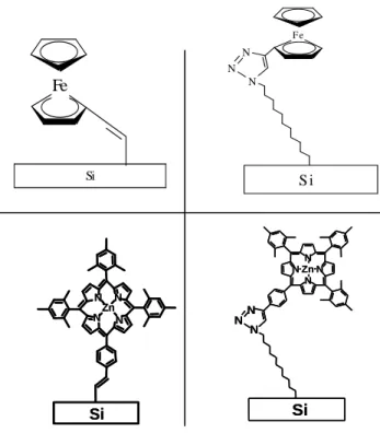
To be in direct connection with experimental investigations, we have studied grafted systems with ferrocene (Fc) and Zn TPP (Tetra Phenyl Porphyrin), shown schematically in figure 0.8.
Figure 0.8. Ferrocene and ZnTPP grafted on Si surface. 1) Fc-direct covalent bond 2) Fc -covalent bond with N3(CH2)111inker 3) ZnTPP –direct covalent bond 4) ZnTPP- covalent bond with N3(CH2)111inker
Due to the hybrid nature of the systems, two approaches were developed. One was based on a molecular description of the whole system, where the Si surface was modelled by a Si aggregate. We used quantum chemistry through DFT methods, leading to a MO (molecular orbital) description of the hybrid systems which give important informations about Homo-Lumo gaps, charge localization or bonding properties. Neverthless, a MO description is very accurate especially for isolated molecules, but not well adapted for the description of infinite surfaces.
N N N N Zn Si N N N N Zn Si Si N N N N Zn N NN Si N N N N Zn N NN N N N S i F e Si Fe
The other approach was thus based on solid state physics (collaboration with Philippe Blaise, CEA/ LETI), and the last part of my thesis was thus focused on periodical calculations. We have started with the reconstruction of the semiconductor Si surface in order to avoid the gap problem (surface confinement) [48]. Then simulations of chosen molecules grafted on ‘infinite’ Si surface were carried out in order to obtain projected density of states (DOS) of periodical calculations. We thus confronted the MO results with the periodical ones and with experimental data.
Some issues that were addressed in this thesis were: is a MO model made up with an aggregate able or not to describe the main features of such hybrid systems? Which
moleculesexhibit electronicfunctionalities? What is the influence of the linker?Which is
the interaction between the molecules grafted (if it is)? How the energy levels of the molecules penetrate the valence band of Si semiconductor surface?
Both theoretical approaches that were used in this thesis, can offer some answers to these questions. The resulting relevant electronic properties certainly can contribute to a better understanding in analyzing the electronic transport properties of new hybrid silicon/molecular devices.
To summarize, the main objectives of this thesis were the following:
• to model and characterize individually the redox molecules who are interesting for
molecular electronic devices;
• to analyze and describe the electronic properties of the hybrid molecular/silicon
systems;
• to investigate the influence on the charge transfer of molecular structures, of the
linker, or even the substrate itself;
• to investigate the stability of redox molecules (linked directly and indirect) that
covalently bond to Si substrates;
• to propose the optimum strategies for theoretical investigation of such molecular


![Figure I.3 Non-Volatile Memories emerging evolution [28]](https://thumb-eu.123doks.com/thumbv2/123doknet/12885718.370285/60.892.185.759.691.1023/figure-i-non-volatile-memories-emerging-evolution.webp)
