HAL Id: hal-00444354
https://hal.archives-ouvertes.fr/hal-00444354
Submitted on 24 Feb 2010
HAL is a multi-disciplinary open access
archive for the deposit and dissemination of
sci-entific research documents, whether they are
pub-lished or not. The documents may come from
teaching and research institutions in France or
abroad, or from public or private research centers.
L’archive ouverte pluridisciplinaire HAL, est
destinée au dépôt et à la diffusion de documents
scientifiques de niveau recherche, publiés ou non,
émanant des établissements d’enseignement et de
recherche français ou étrangers, des laboratoires
publics ou privés.
Organometallic precursors as catalyst to grow three
dimensional micro/nano structures: spheres, clusters
and wires
M. Sacilotti, Pierre Cheyssac, Gilles Patriarche, J. Decobert, Th.
Chiaramonte, L.P. Cardoso, M.F. Pillis, M.J. Brasil, F. Iikawa, M. Nakaema,
et al.
To cite this version:
M. Sacilotti, Pierre Cheyssac, Gilles Patriarche, J. Decobert, Th. Chiaramonte, et al.. Organometallic
precursors as catalyst to grow three dimensional micro/nano structures: spheres, clusters and wires.
Surface and Coatings Technology, Elsevier, 2007, 201, pp.9104. �10.1016/j.surfcoat.2007.03.056�.
�hal-00444354�
nanostructures: Spheres, clusters & wires
M. Sacilotti
a,⁎
, P. Cheyssac
b, G. Patriarche
c, J. Decobert
d, Th. Chiaramonte
a,e, L.P. Cardoso
e,
M.F. Pillis
a,f, M.J. Brasil
e, F. Iikawa
e, M. Nakaema
e, Y. Lacroute
a, J.C. Vial
g, F. Donatini
gaCouches Minces et Nanostructures group FR 2604CNRS & ICB-UB-Dijon France bLPMC-CNRS-Université Sophia-Antipolis Nice, France
cLPN-UPR20 CNRS, Route de Nozay, Marcoussis, France dAlcatel-Opto+, Route de Nozay, Marcoussis, France e
LDRX & GPO IFGW INICAMP 13083-970 Campinas, L. Optica-Unicamp-Campinas, SP, Brazil
f
IPEN/CNEN-SP, CCTM São Paulo, Brazil
g
LSP-Université Joseph Fourrier Grenoble, France Available online 6 April 2007
Abstract
This paper presents the growth and characterization of three-dimensional structures using metal-organic (or organometallic) chemical precursors like M(CH3)3, where M is a metal. Their morphology depends principally on growth temperature and conditions at the surface of the substrate. These 3D structures can be separated into two classes: i) one with (Ga, Al, In) metallic alloys shaped as sphere, sceptre or cylinder and a carbon membrane covering the alloy; ii) the other with semiconductor or oxide nanowires capped by a metallic sphere. The metal-organic precursors can be seen as catalysts molecules that grow semiconductors with micro and nanostructures similar to the role of gold particles used to grow nanowires in the VLS mechanism. We present the MOCVD growth of Ga2O3, CuGaxOyand (Ga,In)P nanowires using the metal-organic precursors on metallic or metal containing substrates.
© 2007 Elsevier B.V. All rights reserved.
Keywords: Nanostructured materials; MOCVD; Trimethyl-gallium; Nanocrystals
1. Introduction
Production of nanostructured materials is currently an expanding field seeking new routes for its realization and research for understanding the underlying mechanisms. Since Middle Ages, alchemist could produce nanostructured materials embedded in churches' stained glasses. Their colours depend on the glass composition and preparation conditions: particle size, shape and surrounding material [1]. In the same way and for long time ago, carbon nanostructured materials have been obtained by acetylene and/or carbon dust burning in chimney industry[2]. The most important discovery and more present application of nanostructured materials fabrication came in the
sixties with the work of Wagner&Ellis, they produced wire shaped silicon structures (3D-S) with diameter in the microm-eter range[3]. Their method is currently called vapour–liquid–
solid mechanism (VLS). It is based on a metallic cluster deposited on the substrate surface prior to the injection of“food nutrients”: chemical elements that will be incorporated in the 3D-S through a catalysis effect due to the action of a gold cluster as“cooking agent”. In other words, a metallic cluster acts as a catalyst, transforms food nutrients and builds the 3D-S. Following Wagner&Ellis work, many groups: Iijima, Samuel-son, Lieber, and Buhro's[4–7]developed very interesting and intriguing nanostructured materials based on the VLS method. However, and following other routes, nanostructured materials have been grown without metallic cluster as starting point. In this way ferrocene has been utilised as catalyst and an oxide assisted growth has also been realized by others groups: Pinault, Lee and Shi[8–10]. Nevertheless, the actual growth mechanism
⁎ Corresponding author. Université de Bourgogne, 9 avenue A. Savary, BP 47870, 21078 Dijon Cedex France. Tel.: +33 3 80395908; fax: +33 3 80396013.
is still a matter of debate. Most of the discussions about it suffer from considerations related to the size of the metallic cluster, its shape and structure. The size effect is associated to the lowering of the melting point of a metallic cluster when its size decreases
[11–13]. In the same sense and without explanation of the actual mechanism taking place, our group proposed a different way for building 3D-S micro/nanometer sized materials, based on interactions of organometallic precursors with many different substrates and structures deposited on them[14,15]. This paper presents the most important and recent results dealing with 3D-S growth by interaction of organometallic (OM) with substrates containing metal on its surfaces or metallic substrates. It is organised as follows: results of interaction of OM on metallic Cu and kanthal (Fe–Al–Cr alloy) substrates and metal containing InP substrates. Characterizations by using scanning electron microscopy (SEM) and transmission electron micros-copy (TEM) techniques are presented. Discussion and sugges-tion about the present method and comparison with already published growth mechanisms will be presented.
2. Experiment
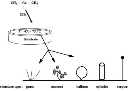
Growth of 3D-S using OM precursors is presented inFig. 1; it is performed by exposition and interaction of OM vapour pressure with a substrate within a MOCVD apparatus[14]. The 3D-S shape and composition obtained after growth depend on several parameters: type of OM precursor (e.g. trimethyl-gallium, TMGa flow∼1 sccm), substrate composition, type of carrier gas (N2: 2–10 slm), growth temperature, reactor pressure
(50–760 Torr) and relative partial pressure of carrier gas/OM. For most cases, amorphous carbon membranes coming from the CH3 OM radical surround the grown 3D-S. As depicted in
Fig. 1, at low temperature, 450–550 °C, we observed the growth
of thin leaves-like structures that we call 3D grass structures. These carbon branched structures are impregnated by Ga when
the OM precursor is TMGa. At relatively higher temperature, 600–750 °C, we obtain 3D-S such as balloons and cylinders (Fig. 1). By using an intermediate temperature, 550–600 °C,
and low carrier (N2) gas flow 3D-S neurone like structures are
obtained, i.e. Ga enveloped and interconnected by carbon membranes and branches (Fig. 1). All these structures contain-ing liquid Ga can be appropriately annealed under NH3 and
form GaN nanocrystals for which light emission is in the visible light spectra [14,16,17]. The above mentioned 3D-S growth takes place on relatively stable substrates such as Si, sapphire, SiO2and quartz. When metallic substrates or metal containing
substrates are used, we obtain wires of oxide single crystals and III–V semiconductors. We call these structures 3D-S sceptres (Fig. 1). Some of these grown structures on metallic or metal containing substrates will be described below.
3. Growth of oxide wires: CuGaxOy/Cu substrates
To facilitate subsequent sample characterization TEM copper grids were used as substrates and exposed to TMGa OM precursor flow to grow (Cu, Ga) oxides. These Cu substrates were cleaned up by conventional techniques but copper oxide always remains at the surface. Doing so, OM interaction takes place in the presence of copper and oxygen. After 15 min exposition of the grid to TMGa flow, sceptre-like structures are present and fixed to the surface of the substrate, as shown inFig. 2. It presents HRTEM picture of a CuGaxOy3D
sceptre-like structure grown on Cu, exposed to a 1 sccm TMGa flow. The inset is a selected area electron diffraction pattern of the wire. An arrow indicates the growth axis of the wire. All diffracted spots can be indexed as instead of in the CuGa2O4
cubic phase— Fd3m (b111N inter-planar distance is 0.47 nm). Diffuse rings of diffraction pattern, although not shown here, are observed and prove that metallic balls of sceptres are amorphous. EDX analysis (not shown) shows the presence of
Fig. 1. Picture representing 3D structures grown by exposure of a substrate to a TMGa organometallic precursor flow (∼1 sccm). Carrier gas flow: N2: 2–10 slm. Its growth depends on the reactor conditions (50–760 Torr), giving rise to grass leaf (450–550 °C), neurone (550–600 °C), balloon, cylinder and sceptre (600–750 °C) shaped structures. Most of these structures are held by carbon membranes, and contain Ga inside. Growth duration is 5 to 15 min.
(Ga, Cu) in the ball and of Cu, Ga and O in the nanowire structure as the main elements. Surprisingly and differing from published data [3,5,6,13], the interface between top ball and wire can be flat or rounded, as depicted inFig. 2. Published data consider a flat interface between the wire and the ball, where these data consider only results after the end of the growth of the wire. Moreover, the geometry of the interface may be different during growth, at high temperature and before the total quantity
of ingredients of the ball are consumed; these ingredients come presumably by surface diffusion instead of volume diffusion
[13,18]from the environment during growth.
4. Growth of oxide wires: Ga2O3/kanthal substrates
When metallic kanthal (Fe, Al, Cr alloy) substrates are used and exposed to a TMGa OM flow, we observe the growth of sceptre-like shaped 3D-S, (Fig. 3). The top ball is made of Ga and the wire of gallium oxide, as observed by EXD (not shown) and TEM measurements. From the selected area of electron diffraction TEM patterns (Fig. 3), we have established that wires are single crystals composed of gallium oxide identified as the monoclinic Ga2O3phase (space group C2/m with a = 1.223 nm,
b = 0.304 nm, c = 0.580 nm andβ=103.7°). Note that the wire shown inFig. 3is not entirely filled and can be considered as a tube. Kanthal alloys can be utilised for home heating apparatus, they are metal alloys exhibiting a high melting point. At growth temperature, 650 °C, we do not know which of its oxide surface reacts with TMGa to grow Ga2O33D-S.
Fig. 2. a) High-resolution TEM bright field picture, and selected area electron diffraction pattern inset of a CuGa2O4 wire grown on Cu at 650 °C during
15 min b) and c) HRTEM bright field image of CuGa2O4 nanowire single
crystals. Note that the interface between wire/ball and top of the ball can be (a) flat/round; (b) round/flat; (c) round/round.
Fig. 3. a) SEM picture of nanostructures grown on kanthal (Fe–Al–Cr alloy). b) Dark field TEM picture of a single wire in selected area mode. Electron diffraction pattern modes TEM picture of Ga2O33D structures grown on kanthal
5. Growth of III–V compound wires: GaInP and GaP on InP substrates
Metal-organic molecules can be used to grow 3D structures directly on polycrystalline or single crystal InP substrates by the MOCVD technique. The growth temperature varied from 600 to 700 °C, a range where the surface of InP substrates should start to decompose in a non-congruent way, leaving free metallic In on its surface[19]. Trimethyl-gallium (TMGa) and/or trimethy-lindium (TMIn) were utilised to grow wire-like structures; N2
(2–5 slm) was the carrier gas in a MOCVD vertical reactor. These presented 3D structures that have a sceptre-like shape (wire-like) and are made of a long GaInP or GaP rod support, capped by a metallic ball as depicted in Fig. 4. Equations of growth of these structures are given below.
TMGaþ InP þ ð650 -CÞ→GaInP wire capped by ðGa; InÞ ball þ carbon radicals
TMGaþ TMIn þ InP
þð650 -CÞ→GaP wire capped by ðGaÞ ball þcarbon radicals
The exposure of InP to the flow of TMGa molecules, 3D-S of GaInP (In∼63%) is obtained. High-resolution TEM images show that wires have the structure of GaInP single crystals
(Fig. 4a). Many crystal structures grow alongb111N and b311N rod axes. Crystals twined along the direction of growth are observed, as shown in Fig. 4a. Bamboo-like structures are observed among these 3D structures.b111N oriented wires are twined along the growth direction (60° rotation of each slice of the wire). Metallic balls on top of sceptres are mostly In, as detected by EDX (not shown). The whole 3D sceptre structure is externally made of an amorphous layer of gallium oxide as shown inFig. 4a. In the present case, In and P comes from a non-congruent In and P evaporation of InP above 350 °C.
Surprisingly, simultaneous exposure of InP substrates to a TMGa flow and to a TMIn vapour pressure creates GaP wires, as presented in Fig. 4b. These wires are b111N oriented and twined within the growth direction (60° rotation of each slice of the wire). At the present stage, we do not know why an addition of TMIn inhibits the formation of In containing wires. In the present case, Ga comes from TMGa decomposition and P from InP non-congruent evaporation between In and P.
6. Conclusions
Differently from the VLS (not yet completely explained) growth mechanism, the present results show that wire-like structures can be obtained by exposing different kinds of substrates to a metal-organic precursor flow. VLS method uses a metal deposited prior to the growth of 3D structures. Metallic substrates exposed to OM flow give rise to oxide wires, while that of III–V InP substrates lead to III–V InGaP or GaP wires. An intriguing situation occurs for InP substrates: exposure to TMGa flow created GaInP wires while exposure to TMGa and TMIn led to GaP wires. At the present stage, in comparison with the VLS method, the intriguing growth mechanism is to be developed[3–
8,13]. Substrates surface oxides that are present can participate to the growth of wires but the actual growth mechanism is still a matter of debate [9,10,13]. Organometallic precursors act as catalysts to grow 3D structures. We do not know if the exposure of substrates to the organometallic flow can initially build a metallic nanocluster on its surface, before the wire grows, as for the VLS technique. Certainly, size effects (and curvatures effects) due to metallic nanoclusters play an important role in interactions with substrates and should be taken into consideration for a better understanding of the growth mechanism[11–13]. Nevertheless, the present results can be added to the panorama of many growth methods to be improved and studied to grow nanowires structures without many experimental steps.
Acknowledgements
This work was accomplished under contract, project title FILIMON35 no. ANR-05-NANO-016-03 France, and Brazilian Agencies: Capes, CNPq and Fapesp (proc. N. 05/55861-4) Brazil. References
[1] P. Jain, I. El-Sayed, M. el-Sayed, Nanotoday 2 (2007) 18. [2] M. Biercuk, N. Mason, C. Marcus, Nano Lett. 4 (2004) 1. [3] R. Wagner, W. Ellis, Appl. Phys. Lett. 4 (1964) 89. [4] S. Iijima, Nature (Lond.) 354 (1991) 56.
Fig. 4. a) HRTEM pictures of a bamboo shaped GaInP, case of InP exposed to TMGA flow, (SEM inset on the left) and b) HRTEM picture of a GaP wire made of twined single crystal nanostructure, case of InP exposed to TMGa and TMIn flow. Both structures are grown on InP by MOCVD at 650 °C during 15 min.
[5] B. Ohlsson, M. Bjork, M. Magnusson, K. Deppert, L. Samuelson, L. Wallenberg, Appl. Phys. Lett. 79 (2001) 3335.
[6] X. Duan, Ch. Lieber, Adv. Mater. Weinheim, Ger. 12 (2000) 298J. Am. Chem. Soc. 122 (2000) 188.
[7] H. Yu, J. Li, R. Loomis, L. Wang, W. Buhro, Nature (Lond.) 2 (2003) 517. [8] M. Pinault, V. Pichot, H. Khodja, P. Launois, C. Reynaud, M. L'Hermite,
Nano Lett. 5 (2005) 2394.
[9] S. Lee, N. Wang, C. Lee, Mater. Sci. Eng., A Struct. Mater.: Prop. Microstruct. Process. 286 (2000) 16.
[10] W. Shi, Y. Zheng, N. Wang, C. Lee, S. Lee, Adv. Mater. Weinheim, Ger. 13 (2001) 591.
[11] Ph. Buffat, J.P. Borel, Phys. Rev., A 13 (1976) 2287.
[12] P. Cheyssac, R. Kofman, G. Mattei, P. Merli, A. Migliori, A. Stella, Superlattices Microstruct. 17 (1995) 47.
[13] P. Cheyssac, M. Sacilotti, G. Patriarche, J. Appl. Phys. 100 (2006) 044315. [14] P. Viste, I. Colombier, F. Donatini, J.C. Vial, P. Baldeck, R. Herino, A. Duc-Maugé, J. Godfroy, Y. Lacroute, M. Sacilotti, J. Cryst. Growth 272 (2004) 466.
[15] M. Sacilotti, J. Decobert, H. Sick, G. Post, P. Viste, C. Dumas, G. Patriarche, J. Gryst. Growth 272 (2004) 198.
[16] M. Sacilotti, L. Imhoff, P. Viste, C. Dumas, J.C. Vial, P. Baldeck, I. Colombier, F. Donatini, Jpn. J. Appl. Phys 43 (2004) L698.
[17] M. Sacilotti, L. Imhoff, S. Bourgeois, C. Dumas, J. Decobert, P. Baldeck, I. Colombier, J. Cryst. Growth 261 (2004) 253.
[18] Jonas Johansson, C. Patrik, T. Svensson, Thomas Martensson, Lars Samuelson, Werner Seifert, J. Phys. Chem., B 109 (2005) 13567. [19] M. Sacilotti, R. Masut, A. Roth, Appl. Phys. Lett. 48 (1986) 481.