HAL Id: hal-03008961
https://hal.archives-ouvertes.fr/hal-03008961
Submitted on 17 Nov 2020HAL is a multi-disciplinary open access archive for the deposit and dissemination of sci-entific research documents, whether they are pub-lished or not. The documents may come from teaching and research institutions in France or abroad, or from public or private research centers.
L’archive ouverte pluridisciplinaire HAL, est destinée au dépôt et à la diffusion de documents scientifiques de niveau recherche, publiés ou non, émanant des établissements d’enseignement et de recherche français ou étrangers, des laboratoires publics ou privés.
In Situ X-ray Diffraction Study of GaN Nucleation on
Transferred Graphene
Camille Barbier, Tao Zhou, Gilles Renaud, Patrick Le Fèvre, Frank Glas, Ali
Madouri, Laurent Travers, Martina Morassi, Noëlle Gogneau, Maria
Tchernycheva, et al.
To cite this version:
Camille Barbier, Tao Zhou, Gilles Renaud, Patrick Le Fèvre, Frank Glas, et al.. In Situ X-ray Diffraction Study of GaN Nucleation on Transferred Graphene. Crystal Growth & Design, American Chemical Society, 2020, 20 (6), pp.4013-4019. �10.1021/acs.cgd.0c00306�. �hal-03008961�
1 This document is the unedited Author’s version of a Submitted Work that was subsequently accepted for publication in Crystal Growth & Design, copyright © American Chemical Society after peer review. To access the final edited and published work see https://pubs.acs.org/articlesonrequest/AOR-NZGGPWGIM7AXVWW5ZJQA, see http://pubs.acs.org/page/policy/articlesonrequest/index.html.
In situ X-ray diffraction study of GaN nucleation
on transferred graphene
Camille Barbiera*, Tao Zhoub, Gilles Renaudc, Olivier Geaymondd, Patrick Le Fèvred, Frank
Glasa, Ali Madouria, Antonella Cavannaa, Laurent Traversa, Martina Morassia, Noelle
Gogneaua, Maria Tchernychevaa, Jean-Christophe Harmanda, Ludovic Largeaua
a. Université Paris-Saclay, CNRS, Centre de Nanosciences et de Nanotechnologies (C2N), 10 Boulevard Thomas Gobert, 91120, Palaiseau, France.
b. Center for Nanoscale Materials, Argonne National Laboratory, IL 60439, USA. c. Université Grenoble Alpes, CEA, IRIG-MEM-NRS, 17 avenue des Martyrs, 38000 Grenoble, France.
d. Université Grenoble Alpes, CNRS-Institut Néel, 25 avenue des Martyrs, 38042 Grenoble, France.
e.Synchrotron SOLEIL, L’Orme des Merisiers, Saint-Aubin-BP48, 91192 Gif-sur-Yvette, France
Corresponding Author
* Camille.Barbier@c2n.upsaclay.fr ORCID: 0000-0001-7867-6658
2 ABSTRACT
We investigate by in situ X-ray diffraction the early stage of GaN nanowire growth on a single-layer of polycrystalline graphene transferred onto a Si (100) / SiO2 carrier substrate.
The experiment was carried out in a molecular beam epitaxy chamber installed on a synchrotron line equipped with a X-ray diffractometer and a nitrogen plasma source. The evolution of the in-plane lattice parameters of the crystals is monitored. The in-plane lattice parameter of graphene shows only little variation between room temperature (RT) and GaN growth temperature (720 °C). As for GaN, an incubation time of about 1 h precedes nucleation. Just after nucleation, the GaN nanocrystals are under tensile strain and they relax as growth proceeds. The critical nucleus size and the parameters governing nanowire growth dynamics are obtained from modeling. We discuss the possible incorporation of N atoms in the graphene lattice during the incubation time. These atoms could be involved in chemical bonds between GaN and graphene, which could explain the initial strain observed experimentally.
KEYWORDS: A1. Nucleation, A1. High resolution X-ray diffraction, A1. Growth modelling A3. Molecular beam epitaxy, B1. GaN, B1. Graphene.
INTRODUCTION
GaN-based compounds are among the most coveted semiconductors for applications in optoelectronics and high-power electronics. Though efficient GaN-based devices are nowadays commercially available, the epitaxy of high-quality single-crystalline III-N layers on a low-cost substrate is still challenging. In particular, high electron mobility transistors could benefit from a reduction of the threading dislocation density which is generally quite high in these epilayers1 . Van der Waals epitaxy is an alternative to conventional epitaxy2. This method relies on weak van der Waals interactions between two atomic planes without the
3 formation of covalent bonds between them. Thereby, the deposited layer is expected to be free from epitaxial strain and the amount of defects in the grown structure is expected to decrease drastically.
Several groups have attempted to grow GaN thin films on layered materials such as h-BN3 or graphene4. In these studies, a crystalline substrate (sapphire3, SiC4) was present beneath the layered 2D material. The latter was shown to be efficient for the mechanical peel-off of the epitaxial stack and its transfer on a host support, but the expected reduction of defect density was not achieved: a dislocation density around 109 – 1010 cm-2 was observed3,4. This is possibly due to the underlying crystalline substrate preventing the graphene compliance. Its presence may lead to a situation similar to what happens in conventional epitaxy, via a remote epitaxy mechanism5. Other groups have succeeded in growing GaN nanowires on graphite6,7 and on graphene transferred on single-crystalline substrate8,9,10, or amorphous support11,12. A few of these studies have demonstrated unambiguously that vertical III-V nanowires can grow with a well-defined basal orientation. In-plane alignment was reported on multilayer graphene obtained from SiC7 and on graphene transferred on an SiO212, the GaN < 2110 > directions
being parallel to the graphene zigzag edges. While in the first case, the monocrystalline bulk substrate beneath the layered 2D material may influence the epitaxial alignment, the second case definitely shows that the sole interaction between the 2D material and the three-dimensional (3D) semiconductor can induce an epitaxial stacking. This observation raises the fundamental question of the exact nature of the interaction between GaN and graphene. How do the sp2 orbitals of graphene interact with the sp3 orbitals of GaN at the interface?
This particular material combination presents a large lattice misfit (+29.2%) which seems difficult to fully accommodate by elastic strain. Ref.12 highlights a possible coincidence of the two lattices. Adopting the observed in-plane alignment, a (33) GaN supercell has a moderate misfit with a (44) graphene supercell: namely -3.1 % at room temperature and -2.8
4 % at a growth temperature of 720 °C. If chemical bonds form at the interface, this misfit could reasonably be accommodated via elastic strain at the beginning of growth. Thus, it appears interesting to investigate whether such a strain is present or not during the initial stage of growth. In the present work, we track this hypothetical strain by measuring in situ the lattice parameters of GaN NWs as they start to form on a graphene monolayer transferred on a SiOx
carrier substrate.
EXPERIMENTAL METHODS
The experiments were conducted on the BM 32 beamline at the European Synchrotron Radiation Facilities (ESRF). The beamline is equipped with an ultra-high vacuum growth chamber coupled with a goniometer through a large Be window for X-ray transparency. During this experiment, we have characterized the early stage of the GaN NW growth on a graphene substrate by grazing incidence X-ray diffraction (GIXRD).
The GaN NWs were synthesized by plasma-assisted molecular beam epitaxy (PA-MBE) on a polycrystalline monolayer of graphene transferred on an amorphous carrier substrate. The commercial film used for this experiment was a polycrystalline single-layer graphene, with grain sizes in the tens of micrometers range, grown by chemical vapor deposition (CVD) on a copper foil. The graphene layer was transferred by a wet process from this copper substrate to a 1 cm2 Si (100) substrate covered with a 300 nm layer of thermal SiOx (the transfer procedure
is provided as Supporting Information). This relatively thick layer of amorphous material guarantees that the interaction between the graphene and the monocrystalline silicon carrier substrate underneath is negligible. Before its introduction in the ultra-high vacuum growth chamber, the sample was outgassed at 600 °C for 8 hours in a buffer chamber, in order to eliminate any potential contamination originating from the chemical transfer process. The
5 base pressure in the growth chamber was 5x10⁻¹⁰ mbar before the growth. N-rich conditions were used for the growth of the GaN NWs. The N-plasma source was powered at 350 W with radio frequency and supplied with a 2 sccm N2 flow. From a calibration performed in a
standard MBE chamber in the same conditions, we estimated the N flux to be equivalent to 0.7 monolayer (ML) per second. The Ga effusion cell was heated up to 930 °C, resulting in an atomic flux equivalent to a 0.06 ML/s growth rate on a flat surface. Then, the graphene patch was exposed to Ga and N fluxes simultaneously for 150 minutes. The sample temperature was set at 720 °C, as measured by a 2-waves pyrometer, and the pressure in the chamber was 1.310-5 mbar during growth.
The X-ray energy used during the experiment was 18 keV (0.688 Å wavelength), with a relative energy resolution of 10-4 keV. This energy corresponds to the highest power delivered by the beam line and is much higher than the Ga absorption edge, which avoids most of the fluorescent signal in the measurement. A schematic of the experimental set-up is shown in Figure 1. The incident angle α was set to 0.05° (well below the critical angle for total external reflection) in order to maximize the signal diffracted by the GaN nanocrystals and to minimize the background coming from the carrier substrate. The incident beam spot was 20 μm and 300 μm wide in the directions perpendicular and parallel to the surface, respectively. The beam divergence was 1 mrad and 0.1 mrad, perpendicular and parallel to the surface, respectively. A two-dimensional pixel detector (MAXIPIX, with 1280 256 pixels of 55 55 μm2), positioned at a distance of 700 mm from the sample, was used to map reciprocal space with two possible motions, along β or δ angles (see Figure 1).
6 Figure 1. Schematic of the in situ Nanostructures and Surface (INS) set up at the
ESRF/BM32 beamline, which couples UHV-chamber with a diffractometer.
The in-plane lattice parameters, associated to the crystallographic planes perpendicular to the sample surface, were measured by scanning the detector along the δ angle. The signal was integrated over 5° out-of-plane to increase the counting statistics. These radial scans allowed us to investigate in situ the in-plane deformation of the two materials at the early stage of the growth. The GaN out-of-plane lattice parameter was measured by scanning the detector along the β angle. This second configuration was used to characterize the system after growth by performing a wide out-of-plane reciprocal space mapping (RSM). Finally, the presence of GaN nanocrystals grown on graphene was confirmed by ex situ scanning electron microscopy (SEM) using a ZEISS-Ultra 55 instrument.
RESULTS
Since the transferred graphene is polycrystalline, all the in-plane directions are expected to be equivalent for diffraction. Figure 2 shows radial scans around the Bragg angle of {1010} graphene planes, collected at an arbitrary in-plane azimuthal direction. The two sets of symbols correspond to the experimental in-plane diffraction of the polycrystalline graphene at room temperature (RT) and at the GaN growth temperature (720 °C). The data were fitted by pseudo-Voigt functions. For clarity, Figure 2 shows only the fit of the data at RT.
7 Figure 2. Experimental radial scans around the Bragg peak of {1010} graphene planes, before the growth, at room temperature (RT) in black and at the growth temperature (720 °C) in blue. Pseudo-Voigt fit from RT scan in red. The abscissa was converted into lattice parameter and the error bar was calculated by the square root of the number of counts.
Remarkably, the positions and widths of the peaks obtained at room and growth temperatures are very similar. The peak positions correspond to a lattice parameter of 2.447±0.002 Å and 2.445±0.002 Å at RT and at 720 °C, respectively. During GaN growth, radial scans around the Bragg peaks of {1010} planes of GaN and graphene were performed. We scanned alternatively a δ angular range of 0.8° around the graphene Bragg peak for 3 min of acquisition time, and a δ angular range of 2.5° around the GaN Bragg peak for 2 min. Figure 3a shows some typical graphene radial scans collected during the growth process after 30 to 110 min exposure to Ga and N fluxes. For better clarity, we only present scans at 15 min intervals. Figure 3b shows the GaN radial scans collected in situ from 65 min to the end of growth, with 5 min intervals. The experimental data are fitted with a pseudo-Voigt function for graphene and with a Pearson VII function for GaN.
8 Figure 3. In situ experimental radial scans (dots) around the Bragg Peak of (a) the {1010} graphene planes with 15 min intervals and (b) the {1010} GaN planes with 5 min intervals. A new scan for both materials was recorded every 5 minutes. After recording the radial scans, the diffracted peaks were extracted from the 2D image of the detector by integrating the intensity. Fits (lines) correspond to Pseudo-Voigt function for graphene and Pearson VII for GaN. The abscissa was converted into lattice parameter and the error bar was calculated by the square root of the diffracted intensity.
We detect significant diffraction from graphene until the end of the growth. Between the different scans, the graphene peak intensity varies slightly but without any systematic trend. The peak position does not show any clear evolution either. This indicates that the graphene layer remains crystalline and does not suffer severe structural degradation such as the partial
9 etching sometimes reported after long exposure to nitrogen plasma13. The GaN signal appeared after 65 min of sample exposure to the matter fluxes. Then, the diffracted intensity of GaN increases steadily, with a clear shift of the peak position toward smaller lattice parameters during the first 15 min of GaN growth. After this period, the GaN peak position remains fixed until the end of the growth.
After the growth, the GaN nanostructures on graphene were analyzed at RT by performing an out-of-plane reciprocal space map (RSM), shown in Figure 4a. This RSM was built by scanning the in-plane angle δ by 42° and the out-of-plane angle β by 24°, with 0.05° and 3° angular steps respectively. The diffraction from the monolayer graphene is not visible on the map due to the short counting time. All the Bragg peaks of the hexagonal wurtzite GaN structure are found, with no additional contribution, except a diffuse spot which is attributed to the silicon substrate. The GaN Bragg reflections from the different planes, namely {101l}, {112l} and {123l}, are clearly aligned along the Ɩ miller index, which indicates that the GaN crystallites are vertically c-aligned. These peaks extend as arcs centered on the origin of the reciprocal space. This indicates that the growth direction of some GaN nanocrystallites slightly deviate from the normal axis. We have estimated the tilt distribution by measuring the full width at half maximum (FWHM) of the 1011, 112l, 1231, 2031 and 3032 arcs. We obtain a tilt of 5.6°0.4° around the substrate normal. This value is larger than the typical tilt distribution of GaN NWs reported in the literature7,11,12. It could be due to the roughness of the SiOx layer and a non-ideal transfer process of the graphene monolayer on this layer.This
tilt is confirmed by post-growth observations of the samples by SEM (Figure 4b) which show short GaN NWs with diameters between 10 and 30 nm.
10 Figure 4. (a) The reciprocal space mapping as a function of parallel (Qpara) and perpendicular
(Qperp) momentum transfer, performed after the growth of the GaN NWs. The origin of Qperp
and Qpara arrows represent the origin of the RSM. The intensity is in logarithmic scale. (b) ex
situ tilted view SEM image of GaN NWs on transferred graphene.
In figure 4a, we do not observe diffracted rings. This indicates that the GaN volume irradiated by the X-rays is equivalent to a polycrystalline material with a c-axis fiber texture. Note that, with a grazing incidence of 0.05° and a beam height of 20 µm, the probed area is several mm long and thus contains many graphene grains with various in-plane orientations. Hence, although the GaN NWs grow with the same in-plane orientation on a specific graphene grain12, our GIXRD experiments probe GaN NWs of different in-plane orientations, but which all have their c-axis perpendicular to the substrate surface.
DISCUSSION
First, we will comment in detail our measured value of the graphene lattice parameter and its negligible variation between room and growth temperatures. We will then discuss the
11 evolution of the diffracted signal related to GaN growth, as regards peak position, width and intensity.
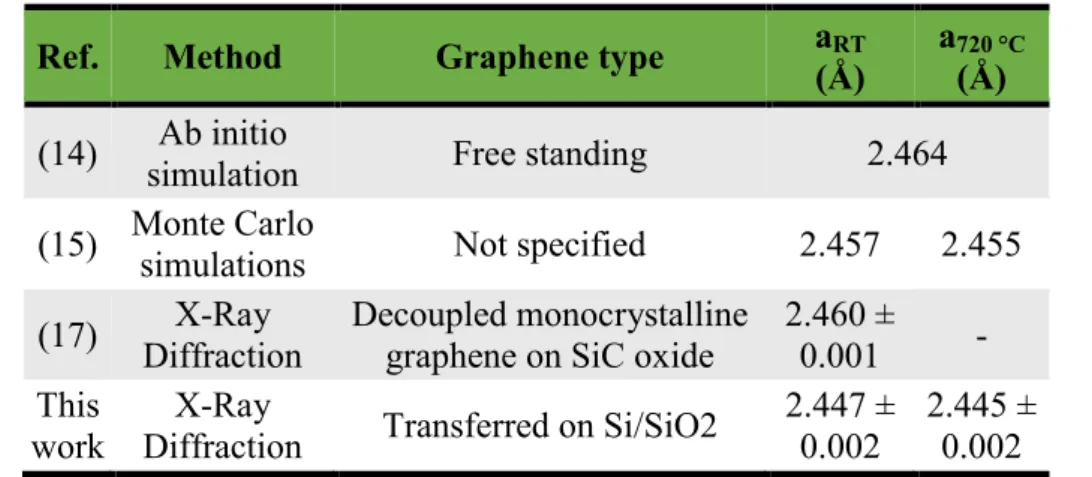
We have measured by GIXRD the average in-plane projection of the lattice parameter of the single-layer polycrystalline graphene transferred on a SiOx substrate. Our experimental value
of 2.447±0.002 Å at RT, is close to those theoretically calculated for free-standing graphene14,15, or measured by scanning tunneling microscopy (STM) on graphene grown on Cu (111)16 and by GIXRD for decoupled graphene on silicon carbide oxide17 (see Table 1).
Ref. Method Graphene type aRT (Å)
a720 °C
(Å) (14) Ab initio
simulation Free standing 2.464 (15) Monte Carlo
simulations Not specified 2.457 2.455 (17) X-Ray
Diffraction
Decoupled monocrystalline graphene on SiC oxide
2.460 ± 0.001 - This
work
X-Ray
Diffraction Transferred on Si/SiO2
2.447 ± 0.002
2.445 ± 0.002
Table 1. Comparison of the graphene lattice parameters obtained by different methods at room temperature and high temperature.
The in-plane lattice parameter that we measure is 0.013 Å smaller than the theoretical graphene lattice parameter of 2.46 Å. It is known that graphene may form ripples or wrinkles and hence may not be totally flat18,19,20. By assuming that our measurements yield the in-plane projection of the actual lattice parameter, a deviation angle of 5.9°±0.5° from the exact surface plane could explain our experimental value smaller than the theoretical one. Furthermore, such a deviation angle is in agreement with the angle of corrugation measured by Meyer et al.21. We can then deduce that our graphene layer is rippled. According to ref. 22, when transferred by a wet process on an amorphous layer, graphene is mechanically free-standing, with no pinning to the carrier substrate22. This is consistent with our observations.
12 Indeed, if the graphene interacted strongly with the SiOx layer underneath, it should at least
partially follow its thermal expansion, which, in turn, is imposed by the thermal expansion of the Si (100) bulk substrate. Between RT and 720 °C, the Si lattice parameter is expected to undergo a thermal expansion of 0.014 Å, corresponding to a relative expansion of ~2.610-3
23
. In the same range of temperature, the graphene peak position does not vary more than 0.002 Å, which corresponds to a relative expansion of 8.110-4. This expansion is thus well below what it would be if graphene followed the thermal expansion of the Si bulk substrate. This indicates that the graphene layer has a thermal free-standing behavior and undergoes no or negligible expansion. Ab initio molecular dynamics14 and Monte Carlo simulation15 have predicted the lattice expansion of free-standing graphene to be between 0.001 Å and 0.003 Å, over this temperature range. Our results are consistent with these values. Actually, the temperature-dependence of graphene structural properties was studied by several groups, mainly by theoretical calculation and Raman spectroscopy experiments. Depending on the simulation method20, the temperature range18,24,25, and the type of substrate19, the reported thermal expansion coefficient of graphene differs widely in sign and value. Our measurement indicates that, between RT and 720 °C, either the thermal expansion coefficient (TEC) always remains very small, or it varies from negative to positive value or the opposite.
From the fits of the in situ radial scans around the Bragg peaks of graphene {1010} and GaN {1010} planes, we extract different quantities, namely the positions, widths and areas of the peaks.
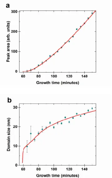
13 Figure 5. (a) Experimental diffraction peak area (blue dots) and fit of the GaN volume (red line) from the nucleation time to the end of the GaN growth. (b) Experimental in plane domain size of the GaN nanowires (blue dots) and fit of the NWs diameter (red line) from the nucleation time to the end of the GaN growth. Both experimental parameters and error bars were extracted from the Pearson VII fits on GaN in situ radial scans.
Figure 5a shows the area of the GaN diffraction peak as a function of growth time. This peak is not detected before 65 min. This delay corresponds roughly to the incubation time during which no GaN nucleus could form. After 65 minutes, the peak area increases with time until the end of the growth. Figure 5b shows the evolution with time of the experimental GaN in-plane domain size (D) extracted (figure 3b) from the width of the diffraction peak. D amounts
14 to about 10 nm shortly after nucleation (65 min) and then increases slowly to reach about 30 nm at the end of growth, in good agreement with our post-growth SEM observations (Fig. 4b). Obviously, the irradiated GaN volume (V) and D increase with time because of the continuous growth of each NW, but the evolution of these quantities may also depend on a distribution over time of the nucleation of the NWs. Modeling the evolution of V and D gives insights into the various parameters involved. Specifically, each NW was assumed to obey the scaling growth model developed by Dubrovskii et al. for single cylindrical NWs26. Namely, if a NW nucleates at time t , its diameter D and height L vary over time t as:
D = D 1 + A(t t ) , L = L D
D (1)
with D and L the dimensions at nucleation and A and α model parameters, which may depend on growth conditions. In addition, we assumed that the total number of NWs varies with time according to an error function law, n(t) = 1 + erf , such that a number dt of new NWs nucleate during dt. At time t , half of the final number of NWs have nucleated and t accounts for the width of the distribution of nucleations over time. In the context of GaN NW growth, other sigmoid functions were employed previously, albeit to describe the “gallium incorporation rate per unit area”, not the NW number or density27,28.The total GaN volume and the average NW diameter are obtained by convoluting functions πD L and D (obtained from Eq. (1)), respectively, with dn dt⁄ (we actually started the integrations at a time t close to the experimentally observed incubation time, at which a number n(t ) of NWs was assumed to form, but this has very little effect on our results). The joint fit of volume and size involves 6 parameters, namely D , A, α, t , t and a parameter aggregating L and N. Figure 5 shows that our model allows us to reproduce the experiments very well. From this, we deduce a NW diameter at nucleation D ≈ 1.5 nm, a characteristic width of the nucleation distribution t ≈ 8 min and a scaling parameter α = 2.49. The values of the fit
15 parameters are expected to depend on growth conditions. This said, the present t falls within the range (up to 15 minutes) obtained by direct measurement of the NW density in other experiments that we carried out at different temperatures. The diameter at nucleation is not accessible experimentally; as expected, our D is below the size of the smallest islands (4 nm) observed by Consonni et al.29 . Our α is very close to the value obtained by Dubrovskii et al. under different growth conditions26, which might suggest that it applies to GaN NWs in general.
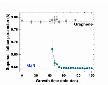
We now focus on the evolution of the GaN and graphene in-plane lattice parameters given by the diffraction peak positions during growth (Figure 3). To confront our results to the coincidence supercell proposed in our previous work12, we plot the evolution of the supercell dimensions 4agraphene and 3aGaN with growth time (Figure 6).
Figure 6. Evolution of the supercell lattice parameters of graphene (grey squares) and GaN (blue dots) during growth. The dashed lines correspond to the average of the (44) aGraphene
(black) and (33) aGaN (blue).
Within the experimental errors, the graphene lattice parameter is constant over the whole duration of the experiment. Note that after growth, only a small part of the graphene area is covered by GaN NWs, so that the diffracted signal is dominated by the uncovered area, i. e.
16 the part which does not interact with GaN. On the other hand, just after nucleation, we observe a rapid evolution of the GaN lattice. The in-plane parameter decreases between 65 and 80 min and then stabilizes at a constant value close to 3.1986 Å ± 0.0006 Å. Within the uncertainties associated to the available data, this value corresponds to the unstrained GaN in-plane lattice parameter at 720 °C30,31,32. This result is compatible with the idea that the upper part of the nanowires is fully relaxed. The initial value after nucleation corresponds to a tensely strained GaN, with a lattice parameter 0.8 % larger than the relaxed one. The rapid evolution suggests strain relaxation, or more exactly, an increasing contribution of a GaN volume adopting its stress-free parameter. It is well established that strain does not build up in the upper part of NWs, even if they are grown on a mismatched substrate33,34. This is why, upon increasing the height of the NWs during growth, the average lattice parameter that we measure tends rapidly to the nominal stress-free value, while at the nucleation stage, only the very first interfacial GaN monolayers contribute to the diffracted signal. Thus, we conclude that GaN nucleates on graphene in a tensile strained state. This suggests that covalent bonding is involved in the cohesion of the interface between graphene and GaN. For a one-monolayer (ML)-high GaN nucleus, the strain should be shared almost equally between the two materials since they have comparable thicknesses. At the growth temperature (720 °C), the experimental lattice mismatch between the (44) supercell of graphene and the (33) supercell of GaN is -2 %. Assuming a 1:1 partition of strain in the two materials of 1 ML height, the GaN and the graphene should accommodate a misfit of about - 1 % and + 1%, respectively. The largest tensile strain detected after nucleation amounts to - 0.8 %. This agrees well with our rough estimate, which does not account for the different elastic properties of the materials. Moreover, the first diffraction measurement after nucleation already corresponds to GaN crystals having on the average more than one monolayer. The strain in GaN observed at nucleation indicates possible covalent bonding between the two materials.
17 However, the exact origin of this bonding remains to be clarified. Indeed, due to its sp2 hybridization, pristine graphene cannot form strong chemical bonds with the first layer of GaN. Nucleation of GaN at pre-existing graphene defects, such as grain boundaries, wrinkles or scratches, is often noticed9,7. Dangling bonds may be associated to some of these defects, which thereby become favorable nucleation sites. However, the fact that, in our conditions, a particularly long incubation time precedes the detection of the first GaN nanocrystals, tends to show that nucleation on pre-existing defects is not predominant. It is more plausible that our transferred graphene was modified upon the N-plasma exposure. This was checked by X-ray photoelectron spectroscopy (see supporting information). This analysis clearly reveals that N incorporates in the graphene lattice before the nucleation of GaN. Nitrogen is a well-known dopant of graphene35,36. Specifically, three main incorporation sites of elemental nitrogen are reported with various proportions, depending on the method employed for doping35,37,38,39,40 : graphitic, pyrrolic and pyridinic, each being bound differently to C atoms. In the pyrrolic configuration, lattice compression was reported41. In our case, we do not observe a graphene lattice distortion associated with this N incorporation, which suggests that the N sites are not dominantly pyrrolic. The incorporation of N atoms in the graphene lattice has a strong impact on its electronic structure. Some configurations may lead locally to sp3 coordination, which could promote the nucleation of GaN by forming a few covalent bonds between the two materials. This scenario also implies local modifications of the graphene lattice parameter under the GaN nuclei. Such modifications cannot be observed in our GIXRD experiments because the diffraction by unstrained graphene surrounding the NWs dominates the signal.
CONCLUSION
Our in situ study of GaN NW nucleation and growth on graphene has focused on the possible interactions between these two materials. We took care to eliminate extraneous interactions by
18 using an amorphous carrier substrate (thermal SiOx). Moreover, in our temperature range, the
transferred graphene behaved as free-standing, with no evidence of thermal stress. As expected for a sp2 material, the graphene surface is weakly reactive under the Ga flux and the N plasma exposure: GaN growth was not detected before a long incubation time. While the graphene remains crystalline over the whole growth process, we argue that it becomes N-doped before GaN can nucleate. At nucleation, GaN is found to be tensely strained with an in-plane extension of 0.8%. This initial strain suggests that covalent bonds are formed at the interface between the two materials. The N atoms incorporated in the graphene lattice before GaN nucleation, might be involved in this chemical bonding. Such a scenario requests further investigation to determine the sites of N incorporation before GaN nucleation, and to identify the signature of a specific interface bonding after GaN nucleation. The measured strain tends to zero as the GaN NWs grow, because of the increasing contribution of their upper parts, which free sidewalls permit efficient lattice relaxation
SUPPORTING INFORMATION:
Details about the graphene transfer process and the X-ray spectroscopy experiment are provided.
ACKNOWLEDGMENT
The authors acknowledge fruitful discussions with Joël Eymery and Christophe Durand from CEA-IRIG in Grenoble. The work has received financial support from ANR "Investissement d’Avenir" through the programs "GaNeX" (ANR-11-LABX-2014), TEMPOS (ANR-10-EQPX-50) and from the EU H2020 ERC project “Nano Harvest” (grant no. 639052).
19 REFERENCES
(1) S. Besendörfer, E. Meissner, A. Lesnik, J. Friedrich, A. Dadgar, T. Erlbacher, Methodology for the investigation of threading dislocations as a source of vertical leakage in AlGaN/GaN-HEMT heterostructures for power devices, J. Appl. Phys. 125 (2019) 095704. https://doi.org/10.1063/1.5065442.
(2) A. Koma, K. Sunouchi, T. Miyajima, Fabrication and characterization of
heterostructures with subnanometer thickness, Microelectron. Eng. 2 (1984) 129–136. https://doi.org/10.1016/0167-9317(84)90057-1.
(3) Y. Kobayashi, K. Kumakura, T. Akasaka, T. Makimoto, Layered boron nitride as a release layer for mechanical transfer of GaN-based devices, Nature. 484 (2012) 223– 227. https://doi.org/10.1038/nature10970.
(4) J. Kim, C. Bayram, H. Park, C.W. Cheng, C. Dimitrakopoulos, J.A. Ott, K.B. Reuter, S.W. Bedell, D.K. Sadana, Principle of direct van der Waals epitaxy of
single-crystalline films on epitaxial graphene, Nat. Commun. 5 (2014) 4836. https://doi.org/10.1038/ncomms5836.
(5) Y. Kim, S.S. Cruz, K. Lee, B.O. Alawode, C. Choi, Y. Song, J.M. Johnson, C. Heidelberger, W. Kong, S. Choi, K. Qiao, I. Almansouri, E.A. Fitzgerald, J. Kong, A.M. Kolpak, J. Hwang, J. Kim, Remote epitaxy through graphene enables two-dimensional material-based layer transfer, Nature. 544 (2017) 340–343.
https://doi.org/10.1038/nature22053.
(6) S.N. Ã, T. Tabata, Y. Honda, M. Yamaguchi, H. Amano, GaN Nanowires Grown on a Graphite Substrate by Radio Frequency Molecular Beam Epitaxy ( b ) 500 nm, 52 (2013) 1–4.
(7) S. Fernández-Garrido, M. Ramsteiner, G. Gao, L.A. Galves, B. Sharma, P. Corfdir, G. Calabrese, Z. De Souza Schiaber, C. Pfüller, A. Trampert, J.M.J. Lopes, O. Brandt, L.
20 Geelhaar, Molecular Beam Epitaxy of GaN Nanowires on Epitaxial Graphene, Nano Lett. 17 (2017) 5213–5221. https://doi.org/10.1021/acs.nanolett.7b01196.
(8) M. Heilmann, G. Sarau, M. Göbelt, M. Latzel, S. Sadhujan, C. Tessarek, S. Christiansen, Growth of GaN micro- and nanorods on graphene-covered sapphire: Enabling conductivity to semiconductor nanostructures on insulating substrates, Cryst. Growth Des. 15 (2015) 2079–2086. https://doi.org/10.1021/cg5015219.
(9) M. Heilmann, A.M. Munshi, G. Sarau, M. Göbelt, C. Tessarek, V.T. Fauske, A.T.J. Van Helvoort, J. Yang, M. Latzel, B. Hoffmann, G. Conibeer, H. Weman, S.
Christiansen, Vertically Oriented Growth of GaN Nanorods on Si Using Graphene as an Atomically Thin Buffer Layer, Nano Lett. 16 (2016) 3524–3532.
https://doi.org/10.1021/acs.nanolett.6b00484.
(10) T. Araki, S. Uchimura, J. Sakaguchi, Y. Nanishi, T. Fujishima, A. Hsu, K.K. Kim, T. Palacios, A. Pesquera, A. Centeno, A. Zurutuza, Radio-frequency plasma-excited molecular beam epitaxy growth of GaN on graphene/Si(100) substrates, Appl. Phys. Express. 7 (2014) 071001. https://doi.org/10.7567/APEX.7.071001.
(11) K. Chung, H. Beak, Y. Tchoe, H. Oh, H. Yoo, M. Kim, G.C. Yi, Growth and characterizations of GaN micro-rods on graphene films for flexible light emitting diodes, APL Mater. 2 (2014) 92512. https://doi.org/10.1063/1.4894780.
(12) V. Kumaresan, L. Largeau, A. Madouri, F. Glas, H. Zhang, F. Oehler, A. Cavanna, A. Babichev, L. Travers, N. Gogneau, M. Tchernycheva, J.C. Harmand, Epitaxy of GaN Nanowires on Graphene, Nano Lett. 16 (2016) 4895–4902.
https://doi.org/10.1021/acs.nanolett.6b01453.
(13) H. Hayashi, Y. Konno, K. Kishino, Self-organization of dislocation-free, high-density, vertically aligned GaN nanocolumns involving InGaN quantum wells on
21 https://doi.org/10.1088/0957-4484/27/5/055302.
(14) M. Pozzo, D. Alfè, P. Lacovig, P. Hofmann, S. Lizzit, A. Baraldi, Thermal expansion of supported and freestanding graphene: Lattice constant versus interatomic distance, Phys. Rev. Lett. 106 (2011). https://doi.org/10.1103/PhysRevLett.106.135501.
(15) K. V. Zakharchenko, M.I. Katsnelson, A. Fasolino, Finite temperature lattice properties of graphene beyond the quasiharmonic approximation, Phys. Rev. Lett. 102 (2009). https://doi.org/10.1103/PhysRevLett.102.046808.
(16) L. Gao, J.R. Guest, N.P. Guisinger, Epitaxial graphene on Cu(111), Nano Lett. 10 (2010) 3512–3516. https://doi.org/10.1021/nl1016706.
(17) T. Schumann, M. Dubslaff, M.H. Oliveira, M. Hanke, J.M.J. Lopes, H. Riechert, Effect of buffer layer coupling on the lattice parameter of epitaxial graphene on SiC(0001), Phys. Rev. B - Condens. Matter Mater. Phys. 90 (2014) 41403.
https://doi.org/10.1103/PhysRevB.90.041403.
(18) N. Mounet, N. Marzari, First-principles determination of the structural, vibrational and thermodynamic properties of diamond, graphite, and derivatives, Phys. Rev. B - Condens. Matter Mater. Phys. 71 (2005) 1–14.
https://doi.org/10.1103/PhysRevB.71.205214.
(19) P.R. Shaina, L. George, V. Yadav, M. Jaiswal, Estimating the thermal expansion coefficient of graphene: The role of graphene-substrate interactions, J. Phys. Condens. Matter. 28 (2016). https://doi.org/10.1088/0953-8984/28/8/085301.
(20) Y. Magnin, G.D. Förster, F. Rabilloud, F. Calvo, A. Zappelli, C. Bichara, Thermal expansion of free-standing graphene: Benchmarking semi-empirical potentials, J. Phys. Condens. Matter. 26 (2014). https://doi.org/10.1088/0953-8984/26/18/185401.
(21) J.C. Meyer, A.K. Geim, M.I. Katsnelson, K.S. Novoselov, T.J. Booth, S. Roth, The structure of suspended graphene sheets, Nature. 446 (2007) 60–63.
22 https://doi.org/10.1038/nature05545.
(22) N. Ferralis, R. Maboudian, C. Carraro, Determination of substrate pinning in epitaxial and supported graphene layers via Raman scattering, Phys. Rev. B - Condens. Matter Mater. Phys. 83 (2011). https://doi.org/10.1103/PhysRevB.83.081410.
(23) Y. Okada, Y. Tokumaru, Precise determination of lattice parameter and thermal expansion coefficient of silicon between 300 and 1500 K, J. Appl. Phys. 56 (1984) 314–320. https://doi.org/10.1063/1.333965.
(24) D. Yoon, Y.W. Son, H. Cheong, Negative thermal expansion coefficient of graphene measured by raman spectroscopy, Nano Lett. 11 (2011) 3227–3231.
https://doi.org/10.1021/nl201488g.
(25) Y.R. Lee, J.X. Huang, J.C. Lin, J.R. Lee, Study of the Substrate-Induced Strain of As-Grown Graphene on Cu(100) Using Temperature-Dependent Raman Spectroscopy: Estimating the Mode Grüneisen Parameter with Temperature, J. Phys. Chem. C. 121 (2017) 27427–27436. https://doi.org/10.1021/acs.jpcc.7b08170.
(26) V.G. Dubrovskii, V. Consonni, L. Geelhaar, A. Trampert, H. Riechert, Scaling growth kinetics of self-induced GaN nanowires, Appl. Phys. Lett. 100 (2012).
https://doi.org/10.1063/1.3701591.
(27) S. Fernández-Garrido, J.K. Zettler, L. Geelhaar, O. Brandt, Monitoring the formation of nanowires by line-of-sight quadrupole mass spectrometry: A comprehensive
description of the temporal evolution of GaN nanowire ensembles, Nano Lett. 15 (2015) 1930–1937. https://doi.org/10.1021/nl504778s.
(28) M. Sobanska, S. Fernández-Garrido, Z.R. Zytkiewicz, G. Tchutchulashvili, S. Gieraltowska, O. Brandt, L. Geelhaar, Self-assembled growth of GaN nanowires on amorphous AlxOy: from nucleation to the formation of dense nanowire ensembles, Nanotechnology. 27 (2016). https://doi.org/10.1088/0957-4484/27/32/325601.
23 (29) V. Consonni, M. Knelangen, L. Geelhaar, A. Trampert, H. Riechert, Nucleation
mechanisms of epitaxial GaN nanowires: Origin of their self-induced formation and initial radius, Phys. Rev. B - Condens. Matter Mater. Phys. 81 (2010) 1–10.
https://doi.org/10.1103/PhysRevB.81.085310.
(30) M. Leszczynski, T. Suski, H. Teisseyre, P. Perlin, I. Grzegory, J. Jun, S. Porowski, T.D. Moustakas, Thermal expansion of gallium nitride, J. Appl. Phys. 76 (1994) 4909– 4911. https://doi.org/10.1063/1.357273.
(31) H.P. Maruska, J.J. Tietjen, The preparation and properties of vapor-deposited single-crystal-line GaN, Appl. Phys. Lett. 15 (1969) 327–329.
https://doi.org/10.1063/1.1652845.
(32) C. Roder, S. Einfeldt, S. Figge, D. Hommel, Temperature dependence of the thermal expansion of GaN, (n.d.). https://doi.org/10.1103/PhysRevB.72.085218.
(33) F. Glas, Critical dimensions for the plastic relaxation of strained axial heterostructures in free-standing nanowires, Phys. Rev. B - Condens. Matter Mater. Phys. 74 (2006) 2– 5. https://doi.org/10.1103/PhysRevB.74.121302.
(34) H. Ye, Z. Yu, Plastic relaxation of mixed dislocation in axial nanowire heterostructures using Peach-Koehler approach, Phys. Status Solidi - Rapid Res. Lett. 8 (2014) 445– 448. https://doi.org/10.1002/pssr.201409072.
(35) H. Wang, T. Maiyalagan, X. Wang, Review on recent progress in nitrogen-doped graphene: Synthesis, characterization, and its potential applications, ACS Catal. 2 (2012) 781–794. https://doi.org/10.1021/cs200652y.
(36) H.M. Jeong, J.W. Lee, W.H. Shin, Y.J. Choi, H.J. Shin, J.K. Kang, J.W. Choi,
Nitrogen-doped graphene for high-performance ultracapacitors and the importance of nitrogen-doped sites at basal planes, Nano Lett. 11 (2011) 2472–2477.
24 (37) F. Joucken, Y. Tison, J. Lagoute, J. Dumont, D. Cabosart, B. Zheng, V. Repain, C.
Chacon, Y. Girard, A.R. Botello-Méndez, S. Rousset, R. Sporken, J.C. Charlier, L. Henrard, Localized state and charge transfer in nitrogen-doped graphene, Phys. Rev. B - Condens. Matter Mater. Phys. 85 (2012) 1–5.
https://doi.org/10.1103/PhysRevB.85.161408.
(38) M. Scardamaglia, B. Aleman, M. Amati, C. Ewels, P. Pochet, N. Reckinger, J.F. Colomer, T. Skaltsas, N. Tagmatarchis, R. Snyders, L. Gregoratti, C. Bittencourt, Nitrogen implantation of suspended graphene flakes: Annealing effects and selectivity of sp2 nitrogen species, Carbon N. Y. 73 (2014) 371–381.
https://doi.org/10.1016/j.carbon.2014.02.078.
(39) M. Rybin, A. Pereyaslavtsev, T. Vasilieva, V. Myasnikov, I. Sokolov, A. Pavlova, E. Obraztsova, A. Khomich, V. Ralchenko, E. Obraztsova, Efficient nitrogen doping of graphene by plasma treatment, Carbon N. Y. 96 (2016) 196–202.
https://doi.org/10.1016/j.carbon.2015.09.056.
(40) N. Soin, S. Sinha Roy, S. Roy, K.S. Hazra, D.S. Misra, T.H. Lim, C.J. Hetherington, J.A. McLaughlin, Enhanced and stable field emission from in situ nitrogen-doped few-layered graphene nanoflakes, J. Phys. Chem. C. 115 (2011) 5366–5372.
https://doi.org/10.1021/jp110476m.
(41) Z. Zafar, Z.H. Ni, X. Wu, Z.X. Shi, H.Y. Nan, J. Bai, L.T. Sun, Evolution of Raman spectra in nitrogen doped graphene, Carbon N. Y. 61 (2013) 57–62.
25 Supporting Information
Graphene transfer process: The single-layer polycrystalline (grain size up to 20 µm) graphene
grown by CVD on copper foil (60 mm x 40 mm) were purchased from Graphenea supermarket. To transfer the graphene patches, from the Cu substrate to 1 cm² Si (100) wafers covered with a 300 nm layer of thermal SiOx, we realized a wet-transfer process. First, the
Cu/graphene foil was spin-coated with a 50-nm-thick layer of poly(methyl methacrylate) (PMMA-A2) to protect the graphene. Then, a 1 cm² piece of Cu/graphene/PMMA was deposited on the surface of a (NH4)2S2O8 bath solution, in order to etch the copper substrate at
the backside. The acid solution was prepared by diluting 2.4 g of ammonium persulfate powder with 100 ml of deionized (DI) water. After 5 hours etching time, the floating graphene/PMMA piece was rinsed into three DI water baths during 10 minutes each, fished with the Si/SiOx substrate and dried in ambient atmosphere. The PMMA layer on top of the
graphene was removed by solvent cleaning (acetone and isopropyl alcohol) and rinsed in DI water. Then, the sample was introduced in the outgassing chamber.
26 Figure A: XPS experimental data on transferred graphene (black) and on transferred graphene exposed 1 hour to the N-plasma (blue).
The impact of the N-plasma on our transferred graphene was characterized by X ray photoelectron spectroscopy realized at Cassiopée beam line of SOLEIL synchrotron, in a previous study. The photon energy was set to 650 eV. In order to analyze the incorporation of N atom, we measured a transferred graphene without exposure to N-plasma (as a reference sample) and a transferred graphene exposed for 1 hour to N-plasma. This exposure time corresponds to the incubation delay of the GaN growth in our system. From the reference sample, only the C-1s peak was present, which was expected. For the graphene exposed to N-plasma, the C-1s peak was still present but also the N-1s peak and weak N-KLL peaks were present. The appearance of these N peaks confirms the efficient incorporation of N atoms into the transferred graphene during the incubation time.