PZT thick films by diol chemical solution deposition
S. Gentil&M. Kohli&A. SeifertReceived: 1 March 2006 / Accepted: 22 August 2006 / Published online: 21 March 2007 # Springer Science + Business Media, LLC 2007
Abstract Process optimization and properties of lead zirco-nate titazirco-nate (PZT) films for piezoelectric micromachined ultrasonic transducers (pMUTs) for scanning probe devices will be presented. The goal of the work was a replacement of the tetragenic and mutagenic solvent and a decrease of time-consuming PZT 2–methoxy ethanol (2MOE) route. An alternative diol-based solution synthesis process was developed and “Design Of Experiment” (DOE) was used to achieve processing optimization for thick and crack free films. Tight parameter control allowed to develop a highly reproducible PZT diol process. The crystallization behaviour of crack-free PbZr0.53Ti0.47O3 films (1–5 μm) with oriented perovskite
structure was examined by X-ray diffraction and surface analysis using scanning electron microscopy. Piezoelectric and dielectric properties were examined. The effective transverse piezoelectric coefficient e31,f of sol–gel processed films was
investigated for 4 μm thick layers. Best properties were achieved with {1 0 0}-textured films, where a remanent e31,f
value of−7.3 C/m2was measured for 4.1μm thick films. Keywords PMUT . PZT film . Design of experiment . Chemical solution deposition . Diol based solutions
1 Introduction
Piezoelectrics are an important family of functional mate-rials in microsystems technology. Their thin film
actua-tion and sensing are useful in devices requiring large output forces, low noise, or high frequency operation [1]. Additionally, planar structures (one level) are able to give excursion and strain detection in the out-of-plane direction, which is very useful for scanning probe devices [2]. Today, there is growing interest for the integration of smart materials with good actuation and/or sensing capabilities, like thin films of Pb(ZrxTi1–x)O3(PZT) and AlN [3]. PZT is
a favorite material when the force or the output charges are of importance, e.g. in piezoelectric micromachined ultra-sonic transducers (pMUTs) for medical imaging and non-destructive materials testing applications, as well as ink-jet printer heads and energy harvesting devices [4,5].
PZT thin films for piezoelectric applications have been investigated for a number of years. Considerable effort has been spent in the development of precursors [6], the development of pure-phase perovskite films [7, 8], and the control of the orientation [9, 10]. The relevant coefficient for ultrasonic devices is the transverse piezo-electric coefficient e31,f, which has to be optimized. It
ei-ther yields the in-plane piezoelectric stress to bend the structure as a function of applied electric field (converse effect), or it yields the charge density as a function of bending strain (direct effect). The index‘f’ of e31,fdenotes
the fact that the film is free to move perpendicular to the film plane (direction 3). As shown in Fig.1, (100)-oriented PbZr0.53Ti0.47O3 thin films have better transverse
piezo-electric properties compared to (111)-textured layers. The film orientation can be controlled with seeding-layers below the PZT film [11,12].
In the past PZT films for piezoelectric applications (0.5– 5 μ thickness) were mostly produced from 2-methoxy ethanol (2-MOE) solvent and the organo-metallic precur-sors Pb(C2H4O2)2 · 3H2O, Zr(OCH2–CH2–CH3)4 and Ti
[OCH(CH3)2]4] [13]. The resulting solutions are not only
toxic, but also need a high number of deposition and annealing steps, due to their low concentration.
J Electroceram (2007) 19:307–310 DOI 10.1007/s10832-007-9053-2
S. Gentil (*)
EPFL-STI-IMX, Ceramic Laboratory, Lausanne, Switzerland e-mail: [email protected] M. Kohli
:
A. Seifert IR Microsystems, PSE-C, Lausanne, Switzerland e-mail: [email protected]This study was undertaken to circumnavigate these disadvantages by using an alternative synthesis route for the production of high quality Pb(ZrxTi1–x)O3films for the use in
pMUT devices. In order to optimize the processing rapidly, “Design Of Experiment” (DOE) was used. This technique is a powerful tool to obtain a maximum of results in a relatively short time with a limited set of well-selected experiments. Three principal processing parameters were chosen and varied to optimize film microstructure and properties.
2 Experimental procedures
2.1 Solution synthesis and chemical solution deposition (CSD) of PZT
Precursor sols for PbZr0.53Ti0.47O3 films were prepared
using 1–3 propanediol solutions with lead acetate trihy-drate, titanium diisopropoxide bis(acetylacetonate) and a zirconium acetate solution, according to diol-based solution synthesis [14, 15] and modified lead zirconate titanate (PZT) film preparation. The route is schematically shown in Fig. 2. All manipulations were routinely performed in normal atmosphere and tight parameter control during solution synthesis resulted in a highly reproducible process. Films deposition was carried out by spin-coating on Si/ SiO2/Ti/TiO2/Pt substrates with seed layers. After three
depositions with subsequent hot-plate pyrolysis, a rapid thermal anneal was employed to crystallize the perovskite phase. This process was repeated until the desired film thickness was achieved.
2.2“Design of experiment” for process optimization DOE was used to rapidly optimize the film deposition parameters to obtain thick and crack free films. Out of the empirical models, also called response surfaces, an equi-radial model (a hexagon also know as “Doehlert Matrix”) was selected [16]. In this model the experimental points are placed on a sphere that can be interactively expanded. The experimental points are normalized from −1 to 1, cor-responding to the minimum and maximum of the experi-mental space. The following three process parameters, also called factors, were selected for process optimization: 1) Pyrolysis temperature, 2) Sol-gel solution concentration, and 3) Spinning-speed during solution deposition. This design required 13 experiments for three factors.
3 Results and discussion
The diol based solution synthesis developed in this study allowed to reduce the synthesis time by 50% compared to 2–MEO solution fabrication, with a solvant (according to the international legislation) being significantly less toxic than the latter. Also, film deposition time was shortened significantly by using the diol route: For the deposition of a Fig. 2 Schematic of the diol synthesis route
0 2 4 6 8 10 12 14 10 20 30 40 50 60 70 PZT (100) PZT (111) -e 31,f (C/m 2 ) composition [Zr]/([Zr]+[Ti])
Fig. 1 Transverse piezoelectric coefficient of (111) and (100)/(001) textured PZT thin films
2μm thick film, only 18 spinning and pyrolysis steps with six crystallization anneals were necessary. Compared to the 2-MEO route, where 32 spinning and pyrolysis steps with eight crystallization anneals were necessary to produce a film of the same thickness, this represents a gain in production time of about 25%. The combined time saving from diol solution synthesis and thin film deposition amount to 33% compared to the 2-MEO process.
The synthesis of PZT diol solutions synthesis was controlled and highly reproducible for solutions with a shelf life of about 2 months.
The DOE program put in place to find the optimal production conditions for the PZT pMUT films required 13 experiments with variations in the designated main factors (pyrolysis temperature, sol-gel solution concentration, and
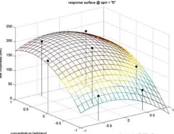
spinning-speed). These experiments were carried out with 3×3 cm2samples and a single crystallization anneal. From the experimental results we received a model for mathe-matical prediction. Analyzing its different effects, we can see that for the thickness model the sol-gel solution concen-tration has the biggest effect and that the spinning-speed can be neglected. Thus, plotting the response surface for the thickness model at fixed spinning-speed (Fig. 3) we can find the optimum in pyrolysis temperature and sol-gel solution concentration for the processing of thick films. However we also need to analyze the crack model. For the crack model only the concentration variation has a relevant effect and the others can be neglected. We found that crack formation occurs at concentrations exceeding the middle of the experimental space. Using the values found from the Fig. 3 Response surface film thickness versus pyrolysis temperature
and sol-gel concentration for fix deposition speed (in the middle of the experimental space). Points correspond to the experimental results
Fig. 4 (a) Cross section, and (b) Top view of PZT film 4.11μm thick
0 100 200 300 400 500 600 700 20 25 30 35 40 45 50 Two Tetha Intensity (100) 92% (110) 2% (111) 6% Pt
Fig. 5 X-Ray diffraction of 4.11μm thick PZT film on PT seeding layer
DOE as a basis, 4 μm films on 4-in wafers were successfully produced.
Scanning electron microscopy (SEM) examination of the film showed columnar grains nucleated at the bottom electrode with an average grain size of about 200 nm. (see Fig. 4). X-ray diffraction of 4.11 μm thick film (Fig. 5) showed phase-pure perovskite with 92% of (100) orientation, also cross-section and plan-view SEM did not show any second phases (Fig.4) The dielectric properties of the films were measured and the best results were found for the 4.10μm thick film. A relative permittivity ofer=1,085 with a dielectric
loss tangent of tanδ=2.3% was obtained, could be compared with Ledermann et al. [12] results for films obtained by 2MOE route and oriented at 87% in (100) direction :er=
1,125/δ=3.8%. The transverse piezoelectric coefficient e31,f
was measured with a cantilever set-up [5] to−7.29 C/m2. 4 Conclusions
With the diol solution synthesis presented in this study, a new synthesis route for PZT CSD, which is less toxic compared to 2-MOE, is now available.
The synthesis of PZT diol solutions synthesis was controlled and highly reproducible for solutions with a shelf life of about 2 months. The synthesis time was decreased by 50% compared to the 2-MEO route. For film deposition we obtained a decrease of working time by 25%, thus resulting in a global process time reduction of 33% compared to the 2-MEO process.“Design of Experiments” was used to optimize the deposition conditions to accom-plish the processing of 4 μm crack-free films on 4-in wafers. Dielectric properties were measured and for the 4.10μm thick film we obtained a permittivity of er=1,085
and a dielectric loss tangent of tanδ=2.3%. The value of the transverse piezoelectric coefficient e31,f=–7.29 is
encour-aging but still needs further improvement by process optimization and possibly doping. This could be another opportunity to apply DOE in a smaller experimental space, optimizing for the transversal piezoelectric coefficient. Acknowledgements The authors gratefully acknowledge the sup-port of the Ceramic Laboratory from STI/IMX/EPFL for technical support and dielectric measurements.
This work was supported by the European FP6––STREP project MUSTWIN no. NMP2-CT-2003-505630.
References
1. P. Muralt, Ferroelectric thin films for micro-sensors and actuators: A review, J. Micromechanics Microengineering 10, 136–146 (2000)
2. Y. Miyahara, PZT cantilever for non-contact atomic force microscopy. Appl. Surf. Sci. 140, 428–431 (1999)
3. P. Muralt, PZT thin films for microsensors and actuators: where do we stand? IEEE Trans. Ultrason. Ferroelectr. Freq. Control. 47 (4), 903–915 (2000)
4. P. Muralt, et al., Study of PZT coated membrane structures for micromachined ultrasonic transducers. IEEE Ultrasonic Sympo-sium. (2001) Atlanta.
5. M.-A. Dubois, P. Muralt, Measurement of the effective transverse piezoelectric coefficient e31,f of AlN and PZT thin films. Sens. Actuators. A 77(2), 106–112 (1999)
6. R.W. Schwartz, Chemical solution deposition of perovskite thin films. Chem. Mater. 9, 2325–2340 (1997)
7. D.V. Taylor, et al., Thickness Dependence of Electrical and Electromechanical Properties of Sol-gel Derived PZT Thin Films. in Electroceramics V. (European Ceramic Society, Aveiro, Portugal, 1996)
8. T. Tani, D.A. Payne, Lead oxide coatings on sol-gel-derived lead lanthanum zirconium titanate thin layers for enhanced crystalliza-tion into the perovskite structure. J. Am. Ceram. Soc. 77(5), 1242–1248 (1994)
9. K.G. Brooks, et al., Orientation of rapid thermally annealed lead zirconate titanate thin films on (111) Pt substrates. J. Mater. Res. 9, 2540–2553 (1994)
10. A. Seifert, et al., Processing optimization of solution derived PbZr1–xTixO3 thin films for piezoelectric applications. Integr. Ferroelectr. 35(1–4), 159–166 (2000)
11. P. Muralt, et al., Texture control of PbTiO3 and Pb(Zr, Ti)O3 thin films with TiO2 seeding. J. Appl. Phys. 83(7), 3835–3841 (1998) 12. N. Ledermann, P. Muralt, et al., {1 0 0}-Textured, piezoelectric Pb (Zrx,Ti1-x)O3 thin films for MEMS:integration, deposition and properties. Sens. Actuators, A. 105, 162–170 (2003)
13. K.D. Budd, S.K. Dey, D.A. Payne, Sol-gel processing of PT, PZ, PZT and PLZT thin films. Br. Ceram. Proc. 36, 107 (1985) 14. M.L. Calzada, R. Sirera, F. Carmona, B. Jimenez, Investigations
of a diol-based sol-gel process for the preparation of lead titanate materials. J. Am. Ceram. Soc. 78(7), 1802–1808 (1995) JUL 15. Y.L. Tu, M.L. Calzada, N.J. Phillips, S.J. Milne, Synthesis and
electrical characterization of thin films of PT and PZT made from a diol-based sol-gel route. J. Am. Ceram. Soc. 79(2), 441–448 (1996) FEB
16. G.E.P. Box, N. Draper, Empirical Model Building and Response Surfaces. Wiley Series in Probability and Mathematical Statistics. (Wiley, New York, 1987), (ISBN 0-471-81033-9)