CMS DAQ Current and Future Hardware Upgrades
up to Post Long Shutdown 3 (LS3) Times
The MIT Faculty has made this article openly available. Please share
how this access benefits you. Your story matters.
Citation
Racz, A. et al. "CMS DAQ Current and Future Hardware Upgrades up
to Post Long Shutdown 3 (LS3) Times." Proceedings of Science 313
(March 2018): 123 © 2018 The Authors
As Published
http://dx.doi.org/10.22323/1.313.0123
Publisher
Sissa Medialab
Version
Final published version
Citable link
https://hdl.handle.net/1721.1/121950
Terms of Use
Creative Commons Attribution-NonCommercial-NoDerivs License
PoS(TWEPP-17)123
CMS DAQ current and future hardware upgrades up
to post Long Shutdown 3 (LS3) times
Attila RACZ1 (2)
CERN
Site de Meyrin, CH-1211 Geneva 23 Switzerland E-mail: [email protected]
Other Authors
Jean-Marc Andre (5), Ulf Behrens (1), James Branson (4), Olivier Chaze(2), Sergio Cittolin(4),
Cristian Contescu (5), Diego Da Silva Gomes(2), Georgiana-Lavinia Darlea (6), Christian Deldicque (2), Zeynep Demiragli (6), Marc Dobson (2), Nicolas Doualot (5), Samim Erhan (3), Jonathan Richard Fulcher (2), Dominique Gigi (2), Maciej Gladki (2), Frank Glege (2), Guillelmo
Gomez-Ceballos (6), Jeroen Hegeman (2), Andre Holzner (4), Mindaugas Janulisa (2), Michael
Lettrich (2), Frans Meijers (2), Emilio Meschi (2), Remigius K. Mommsen (5), Srecko Morovic (2), Vivian O'Dell (5), Samuel Johan Orn(2), Luciano Orsini (2), Ioannis Papakrivopoulos (7), Christoph Paus (6), Petia Petrova (2), Andrea Petrucci (8), Marco Pieri (4), Dinyar Rabady (2),
Thomas Reis (2), Hannes Sakulin (2), Christoph Schwick (2), Dainius Simeleviciusa (2), Cristina
Vazquez Velez(2), Michail Vougioukas (2), Petr Zejdlb (5)
(1) DESY, Hamburg, Germany (2) CERN, Geneva, Switzerland
(3) University of California, Los Angeles, Los Angeles, California, USA (4) University of California, San Diego, San Diego, California, USA (5) FNAL, Chicago, Illinois, USA
(6) Massachusetts Institute of Technology, Cambridge, Massachusetts, USA (7) Rice University, Houston, Texas, USA
a) Also at Vilnius University, Vilnius, Lithuania b) Also at CERN, Geneva, Switzerland
Following the first LHC collisions seen and recorded by CMS in 2009, the DAQ hardware went through a major upgrade during LS1 (2013-2014) and new detectors have been connected during 2015-2016 and 2016-2017 winter shutdowns. Now, LS2 (2019-2020) and LS3 (2024-mid 2026) are actively being prepared. This paper shows how CMS DAQ hardware has evolved from the beginning and will continue to evolve in order to meet the future challenges posed by High Luminosity LHC (HL-LHC) and the CMS detector evolution. In particular, post LS3 DAQ architectures are focused upon.
Topical Workshop on Electronics for Particle Physics 11 - 14 September 2017
Santa Cruz, California
PoS(TWEPP-17)123
CMS DAQ hardware upgrades Attila RACZ on behalf of CMS DAQ Group
2
1. CMS DAQ initial design [1] and upgrades
The initial requirement on the central CMS DAQ was to readout ~1MB of data at 100 kHz level-1 trigger rate (1Tb/s). The main peculiarity of its architecture was to profit from the rapid evolution of the networking technologies in order to build complete events at 100 kHz directly into computer memory without requiring a Level-2 trigger. This feature remains to this day.
Initially, DAQ-1 was interfaced to the detector front-end (~650 data sources) via ~500 custom DAQ cards (FRL for Front End Readout Link) receiving the data over copper cables running the Slink64 [2] custom protocol. The FRL housed a commercial PCI Myrinet card that sent data to the surface where event building and on-line analysis took place.
1.1 First CMS DAQ upgrade [3] LS1 (2013-2014)
During its first long shut down, the LHC was upgraded to provide higher centre-of-mass energy and higher luminosity for Run-2 (2015 to end-of 2018). Therefore, CMS had to prepare itself for higher pile-up and thus higher event sizes (max 2 MB per event after the upgrade). In addition, some of the CMS sub-systems upgraded their detectors and developed new off-detector read-out electronics, based on the μTCA standard, requiring a new interfacing scheme with the central DAQ at a higher bandwidth than in Run-1.
Everything from the Myrinet NIC, housed by the FRL, and upstream was replaced. A custom PCIx card (FEROL, Front End Readout Optical Link) was designed and now receives one or two Slink64 copper stream(s) from the sub-detectors and translates them to fully compliant 10 Gb/s TCP/IP output stream. The translation is entirely implemented inside an FPGA. Alternatively, the FEROL can receive 2x 5Gb/s or 1x 10Gb/s SlinkExpress (optical evolution of Slink64) data streams in order to accommodate new detector readout systems based on uTCA hardware, too small to house the Slink64 bulky copper connector or a mezzanine.
1.2 Second CMS DAQ upgrade LS2 (2019-2020)
No major changes are expected from the detector itself, hence the number of data sources will remain the same with respect to Run2, i.e. ~740 data streams at 10Gb/s under TCP/IP protocol with variable payload. This time, the upgrade will adress mainly aging commercial hardware and switching technologies used for event building where we intend to use network interfaces and switches at 100 or even 200 Gb/s per port. In comparison, DAQ-1 used Myrinet (2.5 Gb/s) and Gb/s Ethernet and DAQ-2 is using 10Gb/s Ethernet and Infiniband FDR (56 Gb/s). An other area of upgrade is to use the same physical computer to perform the data source and data sink functions. In DAQ-1 and DAQ-2, these functions were/are implemented in distinct machines.
2. CMS DAQ for HL-LHC [4] (Post LS3 2024-Q2’2026)
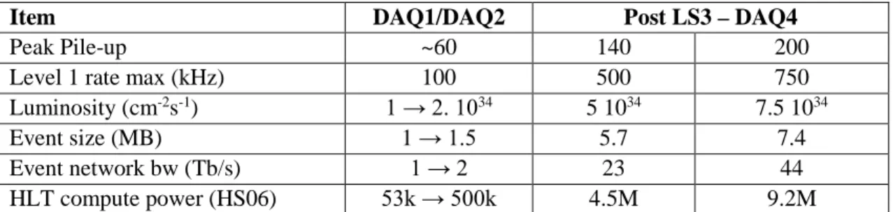
After the LS3 upgrade, the HL-LHC will dramatically challenge the detectors with new conditions, especially the instantaneous luminosity and the multiplicity of the collisions (see Table 1).
After 11 years of data taking and ~20 year lifetime, many detectors of CMS must be upgraded or replaced because of aging and/or non-compliance of their front-end electronic with HL-LHC (pile-up, trigger latency, occupancy). Additional detectors will be installed during LS3 to increase CMS capabilities [5]. All these changes make the readout requirements completely new.
PoS(TWEPP-17)123
Item DAQ1/DAQ2 Post LS3 – DAQ4
Peak Pile-up ~60 140 200
Level 1 rate max (kHz) 100 500 750
Luminosity (cm-2s-1) 1 → 2. 1034 5 1034 7.5 1034
Event size (MB) 1 → 1.5 5.7 7.4
Event network bw (Tb/s) 1 → 2 23 44
HLT compute power (HS06) 53k → 500k 4.5M 9.2M
Table 1 : Evolution of the LHC parameters from Run-1 up to Run-4 starting after LS3 and the expected consequences on CMS event size, total data throughput and on-line computing power.
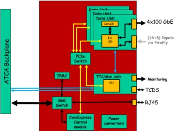
For the design of the new back-end electronics, CMS has chosen the ATCA form factor [6]. Given the presence of hub slots in the ATCA standard, it was natural to think of designing a standard DAQ interface card located in one or both of the hub slots. This card is named the Data and TCDS2 Hub (DTH). The generic functions of the DTH are as follows:
- aggregation of front-end data streams for optimal available bandwidth utilization - translation to a standard switched protocol (i.e. TCP/IP)
- distribution of timing and control signals/messages to all cards present in the chassis - collection and (pre-)processing of each board’s throttling status for fast monitoring and
statistics
2.1 CMS Readout Requirements for HL-LHC (DAQ4)
By going through the different Technical Design Reports produced by all sub-systems for CMS phase 2 (post LS3), the readout requirements can be summarized as follows:
- Total event size : 7.4 MB
- Number of back-end readout cards : ~860 minimum.
- Number of ATCA back-end chassis : ~106 minimum.
- Total throughput at 750 kHz trigger rate : 44 Tb/s
Looking in more detail and especially looking at the average throughput per back-end card and per back-end chassis for each sub-detector, we observe that we have respectivly a range of 45 (from 8 Gb/s-Muon Drift Tubes to 360 Gb/s-Inner Tracker) and 30 (from 70 Gb/s-Trigger to 2.16 Tb/s-Inner Tracker). Such important ranges are impossible to match with a single DTH design as we need also to be globally efficient cost-wise, for CMS and not only for a few sub-systems or DAQ.
2.2 Design considerations for the DTH
Regarding the event data handling, the only way to have a single DTH design that efficiently fits the requirements, on a technical and financial basis, is to implement a modular design. Hence we can think of a single data unit connected to all low throughput data sources of the chassis or multiple data units, each of them being connected to a subset of high throughput data sources of the chassis. This would drive us towards a design with many “little” FPGAs and not a single large FPGA.
Regarding the data connectivity of the DTH with its data sources, we can either use the backplane or fibers routed through the front panel via optical engines. The latter is the only way to have a single DTH design. Moreover, the backplane sets a hard limit of 100Gb/s that is not
PoS(TWEPP-17)123
CMS DAQ hardware upgrades Attila RACZ on behalf of CMS DAQ Group
4
enough for some sub-systems. Finally, signal integrity over large printed circuit boards and backplane connectors at 25 Gb/s is a “challenging” project that cannot be under-estimated.
According to our experience from the FEROL and FEROL-40 [7], we know that the protocol engine that converts SlinkExpress streams to TCP/IP streams requires huge amount of fast memory (i.e at least 10 ms of buffering for round-trip and congestion window) and today the only affordable memories for 100 GbE are serial memories using a significant fraction of the FPGA serdes.
Preliminary analysis of vendor roadmaps indicates that suitable FPGAs, providing enough high-speed transceivers to fit a module with 400 Gb/s input and 4x100 Gb/s outputs in a single component, are available or will soon be available at an affordable price (see Table 2).
KU15P Available PCIGen3 TCDS Memory 4x100G out Serial in Remaining @28G 32 0 0 0 16 16 0 @16G 44 1 2 32 0 8 1
Table 2 : SERDES usage in the context of a data unit for the Xilinx Kintex UltraScale+ KU15P-2.
The input side is implemented with 6 Samtec FireFly [8] chips (4 RX/TX) at up to 28 Gb/s max. A standardization program for optical engines [9] has been started and Samtec is one of the consortium members. Hence, we hope for the future to avoid being “vendor-locked”.
2.3 Data unit capability and
DTH flexibility
Such a data unit will be capable of 4x 100GbE TCP/IP outputs and 24 serial inputs (16 links @28G and 8 links @16G) within the limit of the total 400Gb/s. Early feasibility studies show that we can implement up to 3 data units on an ATCA board (see Figure 1). However, careful and detailed studies must be carried out to confirm this, especially regarding the cooling of such a board.
According to sub-system topologies, we have
to produce 2 flavors of DTH, one with one data unit called the DTH400 and one with 3 data units, the DTH1200. Hence by modulating the mounted/soldered components on the PCB, the DTH can have as few as 1x 100G output (1 data unit equipped with only one 100G optic) and reach 1.2 Tb/s (12x 100G) when all 3 data units are populated. The inputs can range from very little (1x 16G, FireFly sites are left unpopulated) up to the output capacity of the module. The maximum number of inputs per data unit is 24 (8 links@16G and 16 links@28G). However, links at 28G can be operated also at 16G, thus allowing the sub-systems to use low-cost FPGAs for their data sources (FPGA prices are rising dramatically as soon as the serdes are faster than 16G). Hence, with all inputs operated at 16G, 96% of the theoretical ouput bandwidth (384 Gb/s) can be
PoS(TWEPP-17)123
achieved. With the current knowledge of the sub-systems’ topologies, we need 60 DTH400, 51 DTH1200 and 525 100GbE links from the cavern to perform the full readout of the HL-HLC CMS detector.
2.4 Prototyping program
The following is a first attempt to establish a prototyping program in view of LS3 but it will require further coordination with sub-detectors :
- DTH Specifications by end 2017
- First prototype (P1) by mid-2018: will include the ATCA base elements for a hub card, a generic design of the timing/monitoring unit and a functional data module with limited performance (e.g. limited bandwidth and/or number of input/output links).
- Second prototype (P2) by Q2-2020. Will feature a fully functional timing/monitoring unit and one or more fully functional data units. To be used for development of a companion software stack.
- Pre-production units by Q2-2022. To be distributed to detector groups for integration test, local setups, etc. In principle, full functionality and full performance.
- Full production tested and available by end 2023.
3. Conclusions
Since 2009, the CMS DAQ has adapted itself to an evolving detector and LHC conditions. The intermediate hardware layer (FRL) has allowed the decoupling between custom point-to-point data transfers and standard packet switched networks. The sub-detector readout interface has been independent of central DAQ changes. TCP/IP direct from FPGA has enabled the use of efficient balancing layers and different event builder technologies. Seen from the sub-system perspectives, the interface to central DAQ has remained the same compared to 2009, which will continue to be the case. For post LS3 DAQ, the total DAQ throughput needs to gain a factor 40 with respect to DAQ1. A key hardware element for data collection has been presented.
References
[1] The CMS Collaboration, The TriDAS Project, Technical Design Report,
Volume 2: Data Acquisition and High-Level Trigger, CERN-LHCC- 2002-026, 2002. [2] The S-Link 64 bit Extension, A. Racz, R. McLaren, E. van der Bij,
Specification: S-LINK64”, CERN, 2003 [Online]. Available: http://hsi.web.cern.ch/HSI/s-link/spec/ [3] The New CMS DAQ System for Run-2 of the LHC, Tomasz Bawej (CERN) et al.. 2015. 5 pp.
Published in IEEE Trans.Nucl.Sci. 62 (2015) no.3, 1099-1103
[4] CMS Collaboration, “The Phase-2 Upgrade of the CMS DAQ, Interim Technical Design Report”, CERN-LHCC-2017-005 / CMS-TDR-17-005
[5] CMS Collaboration, “Technical proposal for the Phase-II upgrade of the CMS detector”, CERN-LHCC-2015-010 (2015).
[6] https://www.picmg.org/openstandards/advancedtca/
[7] The FEROL 40, a microTCA card interfacing custom point-to-point links and standard TCP/IP Dominique Gigi et al, Poster presented at Twepp 2017 Santa Cruz
[8] https://www.samtec.com/optics/optical-cable/mid-board/firefly