Chemical and Physical Methods of the Templated Direction of Block Copolymers
By
Samuel M. Nicaise B.S. Electrical Engineering University of Kentucky, 2010
SUBMITTED TO THE DEPARTMENT OF ELECTRICAL ENGINEERING AND COMPUTER SCIENCE IN PARTIAL FULFILLMENT OF THE REQUIREMENTS FOR THE DEGREE OF
MASTER OF SCIENCE IN ELECTRICAL ENGINEERING
AT THE
MASSACHUSETTS INSTITUTE OF TECHNOLOGY
SEPTEMBER 2012
0 2012 Massachusetts Institute of Technology. All rights reserved.
The author hereby grants to MIT permission to reproduce and to distribute publicly paper and electronic copies of this thesis document in whole or in part
in any medium now known or hereafter created.
MASSACHUSETTS INST11ITE O TERARIES0C)GY
OCT 2 4 21112
K
B
_____IESignature of Author:
Department of Electrical Engineering and Computer Science August 31, 2012 Certified by:
K',d
P
Karl K. Berggren Associate Professor of Electrical Engineering Thesis Supervisor Accepted by:
/
) rofessor Leslie A. Kolodziejski Professor of Electrical Engineering and Computer Science Chairman of the Committee on Graduate StudentsChemical and Physical Methods of the Templated Direction of Block Copolymers
by
Samuel M. Nicaise
Submitted to the Department of Electrical Engineering and Computer Science on 31 August, 2012, in partial fulfillment of the requirements for the degree of Master of Science in Electrical Engineering at the
Massachusetts Institute of Technology
Abstract
This thesis discusses the investigation of various aspects of templated self-assembly of block copolymer (BCP) thin films for nanofeature fabrication. Two chapters outline the research of a combined physical and chemical templating method with two BCPs. The method was not effective in templating poly(styrene-block-methyl methacrylate) (PS-b-PMMA) BCP because of limited template wettability. The method effectively templated poly(octofluro pentamethacrylate-block-hydroxystyrene)
(OFPMA-b-HSM) BCP to fabricate orthogonally-directed lamellar microdomains and nanohole-mesh arrays. Chapter
4 discusses the achievement of a mean overlay accuracy of 52 nm and 0' for two electron-beam-based lithographic features as a result of an investigated overlay process. Lastly, the thesis reports the fabrication of a wide-range of nanofeatures - from two-dimensional and three dimensional nanoholes arrays to elliptical and cylindrical meshes - by the sacrificial-post templating method with
poly(styrene-block-dimethylsiloxane) (PS-b-PDMS) BCP.
Thesis Supervisor: Prof. Karl K. Berggren
Title: Associate Professor of Electrical Engineering
Acknowledgements
The funding for this thesis work was provided by the DuPont-MIT Alliance, NSF Graduate Research Fellowship Program, MIT Energy Initiative, Semiconductor Research Alliance, and Taiwan Semiconductor Manufacturing Corporation.
This thesis was 2 years of hard, interesting, hair-pulling, and enlightening work. It didn't happen at my hands alone, and required significant input from a large number of other people. To all of them I give considerable thanks and appreciation. Upon the shoulders of giants science sits, and those who perform science are also built only on the foundation of those who support the development of those scientists.
Karl, you have been incredibly important in this process. Your insight never ceases to amaze me and you've had my back at every turn of the process. Not only have you supported my research pursuits, but also your guidance has helped me develop as a student and a professional.
Much thanks to my other professional role models including, but not limited to, Caroline Ross, Ted Fedynyshyn, Hank Smith, Jim Dailey, and Mark Mondol. You have been incredibly open and supportive through every step of the process. Furthermore, all of the teachers of my classes at MIT have been stellar and kept me academically on track.
A special thanks to all of my research "peers", a collection of extremely knowledgeable researchers. I
depended on your intuition, past failures, headaches, and successes. Especially, I cannot thank you enough Amir. Though we didn't always agree, you were one of my most important support beams through this thesis, and I owe you considerably. Beyond Amir, all my friends in the QNN Group and NSL are awesome. You made me realize that I am not in this alone. Lastly, Mauro, you made a hard day easy and a down day up.
Outside of the lab so many friends have made my experience at MIT envious. I absolutely love the comfort and camaraderie of my roommates and cats at Pleasant House. The down-to-earth nature of the Arlington/UMass-Amherst crew is so relaxing. All of my classmates in EECS and around the MIT
campus are way too fun. And of course, the cyclists and triathletes at MIT.. .without you people, I would have quit MIT long ago. You keep me sane and motivated on a daily basis.
Mom and Dad, you are everything to me. All 356 day so of the year I am grateful for how you raised me and the model you have provided. As hard as it is to be geographically so far away from you, I know that you are so proud of me which gives me energy to keep going. Now...if only I could convince you to retire and come to Boston ;)
List of Contents
Chapter 1: Introduction: Block Copolymer Thin Films and their Templated
Self-Assembly
1.1 Block Copolymer Thin Films...16
1.2 Templated Self Assembly of BCPs...
18
1.3 Electron Beam Lithography...23
1.4 Prior Work...
27
1.5 Objectives and Challenges...
28
1.6 Applications...
28
1.7 Overview of Thesis Work...
29
R eferences...30
Chapter 2: Multiple Surface Energy Substrates for PS-b-PMMA Self-Assembly
2.1 PS-b-PMMA Self-Assembly with Surface Energy Modification...33
2.2 Single-SAM Sample Modification for PS-b-PMMA Self-Assembly...39
2.3 Multiple-SAM Sample Modification for PS-b-PMMA Self-Assembly...43
2.4 Conclusions...47
R eferences...49
Chapter 3: Assembly and Direction of a High-Z Polymer
3.1 Discussion of High-f...
51
3.2 Description of Synthesized Polymers...
52
3.3 Thermal Annealing...56
3.4 Chemical Templating...
58
3.5 Physical Templating...
60
3.6 Summary and Conclusion...
66
R eferences...67
Chapter 4: Lithographic Overlay of Negative-tone Resist Features
4.1 Combined Templating Objective...
68
4.2 Investigation of O verlay...
69
4.3 Process D escription...
70
4.4 R esults...73
4.5 C onclusions...
76
R eferences...77
Chapter 5: Sacrificial Templates PS-b-PDMS Self-Assembly
5.1 Prior w ork: D SA of PS-b-PDM S...
78
5.2 Processing Steps...
..
... 79
5.3 PM M A R esist...80
5.4 Tem plating for 2D N anostructures...
82
5.5 Tem plating for 3D N anostructures...
87
5.6 C onclusions...
88
References...90
Appendix I: Contrast Measurement of Neon-Ion-Beam-Lithography with Hydrogen
Silsesquioxane
A .1 Background...
91
A .2 R esults...91
A .3 D iscuss...
93
A .4 Sum m ary...
93
R eferences...95
9List of Figures
Chapter 1: Introduction: Block Copolymer Thin Films and their Templated
Self-Assembly
1.1 Cartoons of different polymers and interaction as BCP...17
1.2 Schematics of different morphologies of BCP...
18
1.3 Phase (or morphology) diagram for conventional BCPs showing the
position of different morphologies hography...18
1.4 Cartoon showing the BCP natural pitch, LO...
.. .... .. .... ... .... . . . .19
1.5 SEMs of thin films of BCP on Si substrates...20
1.6 Schematics of physical and chemical templates of substrates...21
1.7 Schematics of the template preferentiality with respect to different polymer
blocks...22
1.8 Schematics and scanning-electron-micrograph of templates exemplifying
the commensurate condition...23
1.9 Schematics of pattern transfer with BCP...
24
1.10
Schematic
for
fabrication process
of negative-tone
lithographic
features...
... ...
... . ...
25
1.11 Schematic of SEBL microscope column...o ...
26
1.12 Resist Remaining vs. Dose Delivered curve...
...
27
Chapter 2: Multiple Surface Energy Substrates for PS-b-PMMA Self-Assembly
2.1 Schematic diagram of poly(styrene-b-methylmethacrylate)... 33
2.2 Schematics of self-assembled monolayers...35
2.3 Top- and side-view of an ideal example combined templating
m ethod...37
2.4 Major steps of the fabrication process. ...
...
38
2.5
Microscope
image
of a water
droplet on
a
sample in the
goniom eter... ...
.. ...
39
2.6 HSQ Posts fallen over and standing on a substrate...
.
...
40
2.7 SEMs of PS-block of PS-b-PMMA on SAM-coated Si substrate...43
102.8 Top-down scanning electron micrograph of templated PS-b-PMMA BCP
with the single SAM system of BTS...44
2.9 Top-down scanning electron micrographs of PS-block of PS-b-PMMA on
SAM -coated Si substrate...
46
2.10 Scanning-electron micrographs of PS-block of PS-b-PMMA on
SAM-coated Si substrate...
47
2.11 Scanning-electron micrographs of PS-block of PS-b-PMMA on
SAM-coated Si substrate...
47
2.12 SEMs of templated PS-b-PMMA BCP self-assembly with various
different templating schemes...
48
Chapter 3: Assembly and Direction of a High-Z Polymer
3.1 Major Steps of the fabrication process...55
3.2 Top-down scanning-electron micrographs of ObAL60 BCP after different
methacrylate-block removal steps...57
3.3 Top-down scanning-electron micrograph of ObAL60 BCP for different
ramp-down times during thermal annealing...58
3.4 Scanning-electron micrographs of self-assembled thin films of all
synthesized
BCPs
and
measurements
of the BCP
nature
pitches
(LO)...59
3.5 Schematic of line grating array used for chemical templating...60
3.6 Scanning-electron micrograph of ObAL60 templated by a chemical line
grating array as outlined in red...
61
3.7 Schematics of template schemes (a) line-grating array and (b) dot
array...62
3.8
Scanning-electron
micrographs
of ObAL60 with HSQ physical
tem plates...63
3.9 Scanning-electron micrographs of BCPs templated by various physical
tem plates...64
3.10 Top-down scanning-electron micrographs of ObAL80 and ObAL50
templated by short HSQ post-arrays...65
3.11 Top-down scanning-electron micrographs of BCPs templated by various
physical tem plates...
66
3.12 Top-down scanning-electron micrographs of BCPs templated by various
physical tem plates...
67
Chapter 4: Lithographic Overlay of Negative-tone Resist Features
4.1 Schematic of a double pattern of combined chemical and physical
tem plating...70
4.2 Schematics of the first and second write-patterns, and common overlay
errors...71
4.3 Major steps of the fabrication process...72
4.4 Snapshot of the design for the first and second writes...73
4.5 Top-down scanning-electron micrograph example of an overlay of the
first and second write patterns in HSQ without process improvements...75
4.6 Top-down scanning-electron micrograph examples of overlays of the first
and second writes in HSQ after process improvements...76
Chapter 5: Sacrificial Templates PS-b-PDMS Self-Assembly
5.1 M ajor Steps of the fabrication process...
81
5.2 Top-down scanning electron micrographs of PMMA post features...82
5.3 Top-down scanning electron micrograph of a final BCP nanopattern from
hexagonal post template arrays...83
5.4 Top-down scanning electron micrographs of different 2D nanopatterns
formed by the sacrificial-post templating method...84
5.5 Top-down scanning electron micrograph of hexagonal array of nanholes
formed by the sacrificial-post templating method...85
5.6 Top-down scanning electron micrographs of different 2D nanopatterns
formed by the sacrificial-post templating method...85
5.7 Graph of nanohole diameter versus post diameter and pitch...86
5.8 Examples of Matlab steps for determining the size of a-c) generated-holes
and d-f) post-holes...87
5.9 Top-down scanning electron micrographs of 3D nanoholes meshes
templated by the sacrificial-post templating method...89
Appendix I: Contrast Measurement of Neon-Ion-Beam-Lithography with Hydrogen
Silsesquioxane
Al Measurements of the height of HSQ remaining for an example pad
feature...93
List of Tables
2.1 List of the SAMs used in the presented results...36
2.2
Contact angle measurements for a number of different processing
conditions...42
2.3 Contact angle measurements for a number of different processing
conditions...45
3.1 List of common and of-interest homopolymers and their respective
measured surface energies...53
3.2 Characteristics of the different synthesized BCPs...54
Chapter 1: Introduction: Block Copolymer Thin
Films and their Templated Self-Assembly
This thesis summarizes a number of experiments related to templated self-assembly (TSA) of block copolymers (BCPs). The immediate impact of TSA of BCPs is on the science and industry of nanofabrication. Nanofabrication involves the understanding, design, and fabrication of nanoscale patterns, structures, objects and devices. Nanofabrication is important to a variety of different applications, including, but not limited to, nanoelectronics, energy devices, biosensing, plasmonics, nano-electronic and mechanical systems (NEMS) and surface energy engineering-6. Fabrication at the nanoscale is typically carried out in a top-down manner. An example of top-down includes the making the material on the top of a substrate into a particular pattern based on a design. The patterning for this design is typically input from an external machine or system, as opposed to generated from within the material. Alternatively, fabrication at the nanoscale can also be carried out from the bottom up. In this manner, the design evolves from a certain more homogenous material to a structure that has more organization (eg. spatial organization with more periodization, long-range order, or locally complex shapes). Self-assembly is a type of bottom-up nanofabrication. Generally, self-assembly involves smaller components that organize to build a more complex final system. Final systems can include organized domains, objects, or particles of a characteristic size, spacing, and physical/chemical property). Though bottom-up fabrication with self-assembly is typically more difficult to control than top-down fabrication, it is a parallel process, and therefore a faster form of processing for many applications. Furthermore, the characteristics of self-assembly can be more predictable than top-down fabrication. In order to increase the control over bottom-up fabrication, directed self-assembly with top-down-fabricated templates have been investigated. By combining both top-down and bottom-up fabrication, higher throughput, control, and predictability can be achieved.
1.1 Block Copolymer Thin Films
A diblock copolymer (BCP) is a polymer chain comprised of two blocks of two different polymers
covalently bonded in the middle. As is shown in Figure 1.1 a and 1.1 b, a chain of polymer A and a chain of polymer B are bonded in the middle. This bonding makes the polymer chemically inseparable, and therefore the BCP assumes new micro and macro characteristics not present in the two separate polymers. Each of the polymers contributes their distinct chemical, physical and electrical properties. Importantly, when the polymers are chemically dissimilar, the chains will separate such that polymer A blocks are attracted to similar blocks, and polymer B blocks are attracted to similar blocks, as is shown in Figure
1.1 c. In this way, the BCP self-assembles to form regions of mostly polymer A and regions of mostly 7 polymer B. The measure of this dissimilarity of called the Flory-Huggins interaction parameter,
X
.a) Polymer A Polymer B Figure 1.1. Cartoons of
different polymers and interaction as BCP. a) polymer A and polymer B
b) Covalently Bonded are examples of two chemically distinct polymer chains. b)
polymers A and B form a
c) Self -segregation BCP if they are covalently bonded together. c) Many
Majority Polymer Majority Polymer BCP chains near each
Block B Majority Polymer Block B other will self-segregate
Block A such that polymer A is
attracted to polymer A, and likewise, polymer B is attracted to polymer B.
For bulk BCP, different morphologies (or shapes) have been reported. Typical morphologies include spherical, cylindrical, gyroidal, and lamellar (Figure 1.2a). For spherical, cylindrical and gyroidal, one of the two blocks has less volume and forms the morphology's mesh. The second block has more volume, and forms the bulk, surrounding region. For lamellae, both of the blocks have similar volume, and
therefore are layered with alternating blocks. The gyroidal morphology has not been typically used in templated self-assembly or for nanostructure fabrication, and therefore is not highlighted.
a)
Figure 1.2. Schematics of different
U
morphologies of BCP. a)s C G L Morphologies are shown: S: spherical,
IncreasingfA C: cylindrical, G: gyroidal, L: lamellae
b) (and the inverse, G', C' and S'). As the
volume ratio of polymer A is
increased, fA, is increased, these morphology are cycled through8. b) 3-dimensional renderings of different BCP thin film morphologies: (clockwise from top-left) parallel cylinders, perpendicular cylinders, parallel lamellae, and perpendicular lamellae. In a thin film, the orientation in which the polymer microdomains lie with respect to the substrate is important. For example, parallel cylinders are significantly different from parallel cylinders.
Figure 1.3 Phase (or morphology) diagram for conventional BCPs showing the position of different morphologies. The y-axis is the product of
X
and N (the length of the polymer chain). LargerXN
give leads to less disordered region, and therefore the BCP phase-separates more readily. The x-axis is f, the volumetric fraction of block A to the total volume. When fC.PS = 0.5, the blocks are equal volume, and
the morphology is lamellae. When the
Dsreevolume of block A is increased or
decreased, the morphology changes to
0
0A 0 cylindrical and spherical (with asmaller region of gyroidal)8.
The spatial separation between two similar nanodomains (for example, two adjacent spheres in the spherical morphology) is k, the characteristic spacing (aka natural pitch or Lo) (as is shown in Figure 1.4). For the BCPs of interest, LO is 1Os-of-nms and therefore BCPs are useful for nanofabrication9
individual nanodomains is typically half the natural pitch. For nanofabrication, thin films of BCP are used, typically 5-100 nm thick0. This thickness is similar to LO and therefore only 1-3 nanodomains are stacked on top of the substrate, as is shown in Figure 1.2.b with 1.5 nanodomains.
Figure 1.4. Cartoon showing the BCP natural pitch, LO. When the BCP phase-separates, the distance between two blocks is a key characteristics of the resulting self-assembly. This spacing is called the BCP natural pitch or Lo. It is measurable and a key parameter in the
LO
design of templates.1.2 Templated Self Assembly of BCPs
Researchers have investigated methods for overcoming drawbacks of self-assembly such as short coherence length and local defects. When thin films of BCP self-assemble on the substrate, the nanophase separation leads to an increase in order. The ordering of the nanodomains is typically spatially repeated for a few LO, but may not be coherent at longer ranges. As is shown in Figure 1.5.a, a distance of a few-hundred nanometers is ordered BCP, but the ordering does not extend farther. The distance over which this ordering occurs is called the coherence length and long coherence is typically desired for nanofabrication. Furthermore, self-assembly minimizes local free-energy and therefore may result in defects.
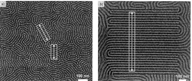
Figure 1.5. SEMs of thin films of BCP on Si substrates. The difference in coherence length is highlighted. a)
SEM of a thin film of self-assembled, untemplated poly(styrene-b-dimethylsiloxane) (PS-b-PDMS) BCP. The
arrowed-boxes show regions of ordered BCP. These regions are small and the length is short. b) SEM of a thin film of self-assembled, templated PS-b-PDMS BCP (template removed). The arrowed-box shows a region of
highly ordered BCP. Compared to a), this region is larger and the length is a longer as a results of the template
directing the self-assembly. For all of these SEMs, thick lighter regions are PDMS-block, and darker interstitial regions the substrate.
Templating the self-assembly of the BCP has been used to increase the coherence length for long-range order and induce local control with reduced defects'1-4. Figure 1.5b shows a micrograph of poly(styrene-b-dimethylsiloxane) (PS-b-PDMS) BCP where the coherence length is increased through the use of templating. Templated self-assembly is capable of increasing coherence length over ultra-large regions.1516 Furthermore, templates can provide complex, local control over the BCP self-assembly. The template type (eg. chemical or physical) and material (eg. polymer brush or organic resist) are the two important characteristics that lead to the control over the BCP self-assembly.
b) TOP VIEW:
Original Chemical Chemical
Modification Pattern
N.V
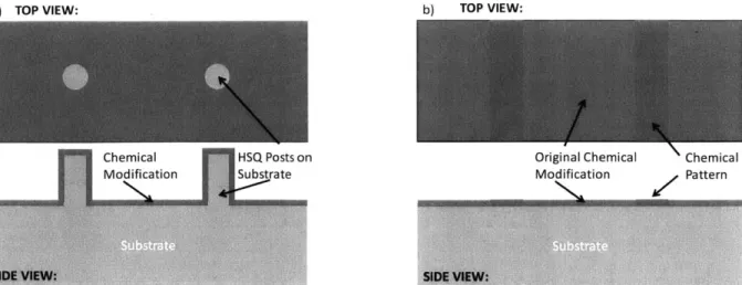
Figure 1.6. Schematics of physical and chemical templates of substrates. a) Top- and side-views of an example physical template on a substrate. In this example, posts of HSQ are patterned on the substrate surface. These posts act as a physical template because a thin film of BCP must assemble around the posts, and therefore the posts physically impede or motivate self-assembly. The entire template is coated with a chemical modification (blue) to give it a uniform chemical nature. b) Top- and side-views of a chemical template on a substrate. In this example, stripes (red) are patterned to be chemically distinct from the surrounding region. These stripes interact with the BCP in a different way than the unpatterned (blue) region and therefore serve as a chemical template.
Firstly, there are two main types of templates, physical and chemical templates which are shown Figure 1.6 schematics. Physical templates are hills, valleys, posts, or holes in the topography of the substrate surface in which the BCP thin film must physically integrate. Chemical templates are regions on the substrate surface that are chemically distinct from the adjacent regions (schematic in Figure 1.6.b). For both templates, the surfaces are typically chemically modified such that one of the two blocks of the BCP has a preference to it. As Figure 1.7 depicts, it will be energetically favorable for the preferential BCP block to face towards the modified surface, and the other block to be repelled by the surface. When this happens, the preferential nanodomain will typically align with the design of the template. Alternatively the substrate surface can be chemically modified to be neutral to both blocks, therefore nonpreferential, and the templating features will be the only preferential regions.
a)
b)1)
Figure 1.7. Schematics of the template preferentiality with respect to different polymer blocks. a) For physical templates, the posts are chemically modified to be preferential to one of the two polymer blocks. In this example, the posts are preferential to the blue block. Therefore, the blue end of the BCP will likely be attracted to the templating post, whereas the red block will be repelled by the post. b) For chemical templates, regions are chemically different than the surrounding regions. In this example the patterned stripes are chemically similar to the red block of the BCP, and therefore attract the red block. They therefore repel the blue block.
Secondly, the template can be commensurate with the natural pitch of the BCP such that the templating features are spaced an integer number of BCP pitch lengths apart (NLo). Examples of this are shown in Figure 1.8. If the template is commensurate with the BCP, the block-preferentiality will drive the BCP to be ordered similar to the template. If the template is not commensurate with the BCP, the preferential block will not line up with the template, and therefore will be strained to "fit" into the template. Achieving a commensurate condition between the template and the BCP will induce long-range order in the BCP self-assembly if the template spans a large area14'7. An example in Figure 1.8a shows a
trench template in which the trench is an integer number of BCP pitches wide (N=4). Similarly, Figure
1.8.b shows a chemical template with chemical patterns that are also an integer number of BCP pitches
template's effect on the local, complex control of the BCP self-assembly, both commensurability and chemical preference seem to play a role.
a) Trench Template
b) Chemical Template
c) Post Template
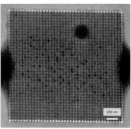
Figure 1.8. Schematics and scanning-electron-micrograph of templates exemplifying the commensurate condition. a) Side-view schematic of a trench template with parallel cylindrical BCP lying within the trench. The trench has a width of 4LO and therefore satisfies a commensurate condition with the BCP (four cylinder nanodomains are directed parallel to the trench). b) Side-view schematic of chemical template with perpendicular lamellae BCP aligning with the chemical patterns. The patterned stripes are spaced by 2Lo and therefore satisfy a commensurate condition with the BCP. c) A top-down SEM of a post physical template array. The x-axis spacing between the posts can be 1L and therefore a single cylinder nanodomain can form over every column of post templates. Blue lines give examples of where the BCP domains may lie within the templating posts.
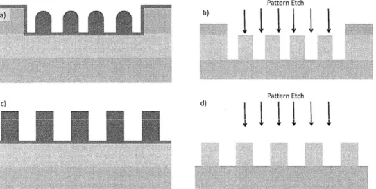
A thin film of self-assembled BCP, templated or untemplated, can serve as a pattern that can be
transferred for the fabrication of other nanofeatures (Figure 1.9) or serve as a functional material. A common pattern transfer process for this application begins with the physio-chemical removal of one of
the two blocks8 1 9. The remaining block can serve as an etch-mask, through which another material below on the substrate can be etched. Furthermore, it is possible for one of the two blocks to be functional (eg. magnetically or electrically), and therefore the thin film serves immediately as an active nanopatterns -a
Pattern Etch
b)
Pattern Etch
c) d)
Figure 1.9: Schematics of pattern transfer with BCP (side-view). a) Most of the majority block (blue) has been physio-chemically removed, to leave only the minority block (red) and the physical template exposed. b) top-down etching can transfer the BCP pattern as well as the template into the underlying material (gold) for a final transferred pattern. c) Similar to (a), the blue block has been removed to leave only the red block. d) This is the same as (b), though in this case, the (chemical) template is removed.
1.3 Electron Beam Lithography
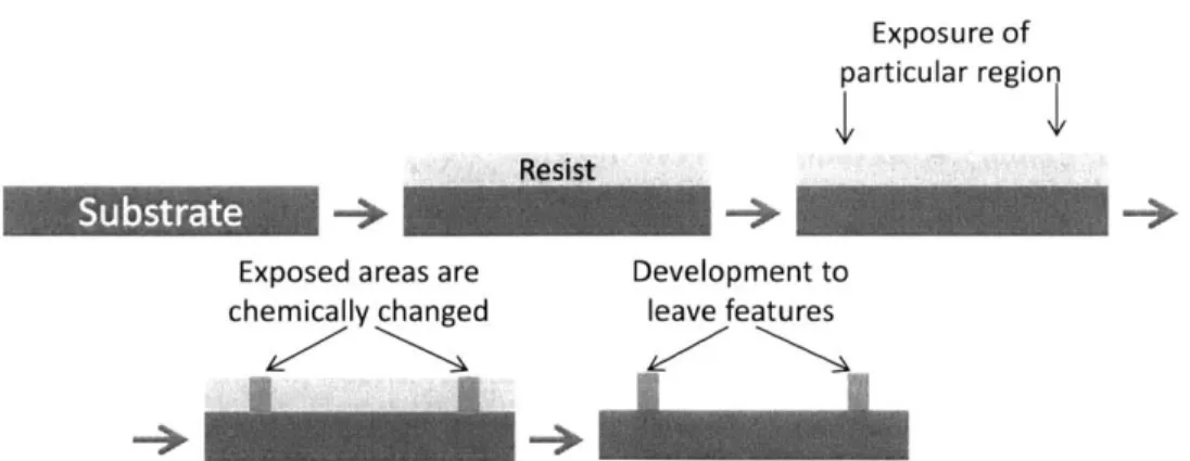
To digress, templates can be fabricated with a number of different methods, and scanning-electron-beam lithography (SEBL) was used predominantly for this thesis. SEBL is capable of making templates of arbitrary design, a large variety of shapes and sizes, and with many different materials. Figure 1.10 shows the major steps of the process for negative-tone lithography, as opposed to positive-tone lithography which is used in other applications. Generally, an organic resist is coated on a planar substrate surface. From the top down, a desired pattern is exposed in the resist by exposure to spatially localized energetic radiation.
Exposure of particular region
Resist
Exposed areas are Development to chemically changed leave features
Figure 1.10: Schematic for fabrication process of negative-tone lithographic features. A substrate has a resist deposited on it in a planar form across the surface. Regions of the resist are exposed by energetic radiation, typically light of a certain wavelength or a beam of particles. The exposed region is chemically changed by this radiation. In the case of negative-tone lithography, this chemical change makes the regions resistant to a developer solution. The solution otherwise washes away the undeveloped regions. This whole process leaves features (posts, lines, pads) on the surface that are similarly shaped to the to-down exposure
Scanning-electron-beam lithography is a form of lithography in which the organic resist on the substrate is exposed by a focused beam of electrons from the top down. The beam is essentially similar to what is used for scanning-electron microscopy and a beam column schematic is shown in Figure 1.11. Electrons are accelerated with a desired voltage away from the electron gun at the top of the gun. As the beam of electrons passes through the gun, the beam is focused by a set of permanent magnet lenses and then steered by another set of lenses. At the bottom, the electron beam collides with the substrate where the energy from the electrons is deposited. As the beam scans an area of the sample, a beam blanker can interfere the path of the electrons in order to selectively expose, or not expose, a region on the substrate.
y
Electron Gun_ Anode
Beam Blanker to turn beam on and off
Lenses to adjust beam current
Lenses to control beam deflection and writing * Objective lens to focus beam
Electron Detectors
- Sample on Stage
Figure 1.11: Schematic of SEBL microscope column. lectrons are accelerated from the electron gun by the voltage generated by the anode. The beam blanker is open or close which allows or prevents the
passage of electrons. A stack of lenses control the current, raster, roundness, writing, and focus of the electron beam as it travels down the column. The beam collides with the sample at the bottom. Other electrons are generated and can be collected in the electron detectors to image the sample.
One important characteristics of the electron beam in SEBL is accelerating voltage. Electrons are accelerated away from the electron gun at high energies, reported as 1-100 keV2
-23
. The electrons collide with the substrate at similar energies, and therefore electrically and physically react in different manners. Lower energy electrons travel slower, have more time to deliver their energy in the resist film, and therefore more efficiently expose the resist. Higher energy electrons travel faster, have less time to deliver their energy to the resist molecules, and therefore less efficiently expose the resist. Alternatively, the interaction volume (three-dimensional region over which the electron deposits its energy) is smaller for high-energy electrons than for low-energy electrons25
. These aspects mean that it takes fewer electrons to expose a region at low-energies, but the features will not be as small as is achievable at high-energies.
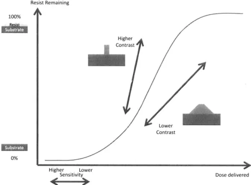
Two important characteristics of the feature fabrication in SEBL are resist sensitivity and contrast, as are shown in Figure 1.12. The sensitivity is the minimum number of electrons required to leave behind some amount of resist (or remove away some resist for positive tone). This has to do with the accelerating voltage and electron efficiency as stated above. Furthermore, other factors impact the sensitivity such as beam-particle type, resist material, and development solution, temperature, time. With higher sensitivity,
the chemical changes of exposure will happen with fewer particles, and an entire design can be patterned relatively faster. Contrast measures the amount of resist left behind as a function of delivered dose. If a small change in delivered dose results in a large change in the amount of resist left behind, then the contrast is high. A high contrast will lead to a more binary exposure process in which exactly the exposed regions result in lithographic features. Alternatively, lower contrast will give features with angled side-wall and more of a grey-scale exposure result.
Resist Remaining 100% esst. 0% Higher Contrast Lower Contrast Higher Lower
Sensitivity Dose delivered
Figure 1. 12: Resist Remaining vs. Dose Delivered curve. For a negative-tone resist, all of the resist is typically washed away during development. As the radiation dose delivered to a region is increased, the amount of resist remaining after development is increased, up to 100% of the original resist thickness. Sensitivity: high sensitivity leaves some resist remaining with a lower dose while lower sensitivity leaves some resist remaining with a higher dose. Contrast: The contrast is represented by the slope of this curve. For higher contrast, a small change in delivered dose results in a large change in remaining resist and lithographic features with steeper sidewalls. For lower contrast, a small change in delivered dose results in a small change in remaining resist and lithographic features with sloped sidewalls. To achieve high resolution lithographic features, higher contrast is desired.
Though the chapters in this theses don't discuss an investigation into the science of lithography, experimental work was dependent on previous advances in lithography technology. Most specifically the work completed at MIT has supported the fabrication of high-resolution features of different materials. A salty developer solution was determined for producing high-resolution features in hydrogen
silsesquioxane (HSQ) resist26. Poly(methyl methacrylate) (PMMA) was found to act as a negative-tone resist (as opposed to the typical positive tone) when exposed to high electron-beam doses". Furthermore, the Appendix specifically discusses the sensitivity of Neon-Ion-Beam Lithography and was supported by previous research in the area of scanning-ion-beam lithography2 7
.
1.4 Prior Work
Significant work has been accomplished in the area of templated self-assembly of BCPs with chemical templates. The canonic example has the chemically patterned region preferential to one of the polymer blocks, and the surrounding region non-preferential, or neutral, to both of the polymer blocks17 28. When
the spacing between patterned stripes was commensurate with the BCP pitch, then the BCP assembled parallel to an array of such patterned regions (similar to Figure 1.8a). Furthermore, when the patterned regions made bends, or junctions, it was possible for the preferred polymer block to follow the bends and junctions.
Also, much research has been performed to template the self-assembly of BCPs with physical templates. Initial work in this area relied on topographical trenches on the substrate in which the BCP would self-assemble" (similar to Figure 1.8b). When the trench width was commensurate with the BCP pitch, the nanodomains ordered well within the trench. This work was expanded to include other types of topographical templates such as atomic crystal edges and other BCPs31
, as well as a large effort in
fabrication of templates with nanoimprint lithography2.
More complex physical templating was introduced in the form of arrays of posts, fences, or holes. These template features occupied key positions within the BCP lattice to provide complex, local control over the self-assembly. In extension, the array of features matched the BCP commensurate condition in
33-34 off-axis directions such that the BCP lattice oriented in this same off-axis direction'
1.5 Objectives and Challenges
The investigation of templated self-assembly of block copolymers is directed towards 3 major objectives and challenges:
Increased Long-Range Order - As was discussed earlier, a thin film of self-assembled BCP doesn't necessarily exhibit long-range order. Templated self-assembly is directed at efficiently and effectively increasing the order over large areas. To increase the impact of this objective, the challenge is to achieve defect-free order over wafer-scale areas with highly-efficient patterning of the templates.
Complex and Local Control - When BCP thin films self-assemble, they can create complex patterns, but control of these patterns requires a template. It is an objective to develop ways to control the BCP locally such that complex patterns can be directed through templating. Research has the challenge of templating the self-assembly of BCPs to achieve bends, junctions and crosses, in single and multiple layers, and with highly local control.
Understanding of Self-Assembly Characteristics - Templates can be used to help understand how BCPs self-assemble. This includes the associated energies of interaction with different interfaces, stress and strain energies, and thermal kinetics. Templating can eliminate certain analytical variables, or provide a larger degree of predictability to test against theory/models. Reverse-engineering of templates is a challenging objective: inputting a desired nanopattern, and using models and simulations to output a needed template to achieve the nanopatterns.
1.6 Applications
Nanopatterns that result from templated self-assembly of BCP have many important applications. They can be used in the fabrication of bit-patterned-media for memory recording devices0. A large application is in the semiconductor fabrication area for manufacturing of integrated circuits. The nanopatterns may be used as mask for the deposition steps in producing transistors and RAM'9. Nanopatterns generated by templated self-assembly have been useful in applications such as nanoelectronics, energy devices,
biosensing, plasmonics, nano-electronic and mechanical systems (NEMS) and surface energy 1-6
engineering
1.7 Overview of Thesis Work
This thesis covers work in the area of templated self-assembly of block copolymers. Each Chapter is a separate investigation, but they each generally relate to one of the above 3 objectives and challenges.
Chapter 2: Multiple Surface Energy Substrates for PS-b-PMMA Self-Assembly - The self-assembly and templated self-assembly of lamellae-morphology PS-b-PMMA is tested on samples modified with a single or two different self-assembled monolayers
Chapter 3: Assembly and Direction of a High-X BCP - The assembly and templated self-assembly of a lamellae-morphology high-X BCP was tested for varying annealing, block-removal, and surface energy characteristics. A wide variety of physical templates was tested with the target of long-range and complex, local control.
Chapter 4: Lithographic Overlay of Negative-tone Resist Features - The overlay metric of the Raith 150 system was determined by patterning of HSQ negative-tone resist patterns in two separate electron-beam-lithography writes.
Chapter 5: Sacrificial Templates for PS-b-PDMS Self-Assembly - Templating of 2D and 3D nanopatterns with PS-b-PDMS cylindrical BCP with PMMA as a sacrificial, negative-tone resist. PMMA was investigated for its removal and effectiveness in replicating similar results with HSQ resist.
Appendix I: Measurement of Neon-Ion-Beam Lithography Contrast Curve - NIBL was tested with HSQ negative-tone resist. Pads were patterned and the remaining HSQ resist was measured by AFM.
These measurements were used to determine the sensitivity of NIBL with HSQ.
References
1. W. Lu, and C. Lieber, Nanoelectronics from the Bottom up. Nat. Mater., 6, 841 (2007).
2. J. Baxter, Z. Bian, G. Chen, D. Danielson, M. S. Dresselhaus, A. G. Fedorov, T. S. Fisher, C. W. Jones, E. Maginn,
U. Kortshagen, A. Manthiram, A. Nozik, D. R. Rolison, T. Sands, L. Shi, D. Sholl, and Y. We, Nanoscale Design to
Enable the Revolution in Renewable Energy. Energy Environ. Sci., 2, 559 (2009).
3. J. L. Arlett, E. B. Myers, and M. L. Roukes, Comparative Advantages of Mechanical Biosensors. Nat. Nanotechnol., 6, 203 (2011).
4. E. Ozbay, Plasmonics: Merging Photonics and Electronics at Nanoscale Dimensions. Science, 311(5758), 189 (2006).
5. J. S. Bunch, Nat. Nanotechnol., NEMS: Putting a Damper on Nanoresonators. 6, 331 (2011).
6. Y. Yang, C. Hsua, T. Chang, L. Kuo, and P. Chen, Study on Wetting Properties of Periodical Nanopatterns by a Combinative Technique of Photolithography and Laser Interference Lithography. Appl. Surf Sci., 256(11), 3683 (2010).
7. Bates, F. S., & Fredrickson, G. H. Annual Block Copolymer Thermodynamics: Theory and Experiment. Review of
Physical Chemistry, 41(1), 525-557 (1990).
8. Reprinted with permission from Bates, F. S., & Fredrickson, G. H., Physics Today, 52(2), 32 (1999). Copyright
1999, American Institute of Physics.
9. Cushen, J. D., Otsuka, I., Bates, C. M., Halila, S., Fort, S., Rochas, C., Easley, J. A. Oligosaccharide/Silicon-Containing Block Copolymers with 5 nm Features for Lithographic Applications. ACS nano, 6(4), 3424-3433 (2012).
10. Hawker, C. J., & Russell, T. P. Block copolymer lithography: Merging "bottom-up" with "top-down" processes.
MRS Bulletin, 30(12), 952-966 (2005).
11. Kim, S. 0., Solak, H. H., Stoykovich, M. P., Ferrier, N. J., De Pablo, J. J., & Nealey, P. F. Epitaxial self-assembly of block copolymers on lithographically defined nanopatterned substrates. Nature, 424(6947), 411-414 (2003). 12. Bita, I., Yang, J. K. W., Jung, Y. S., Ross, C. A., Thomas, E. L., & Berggren, K. K., Graphoepitaxy of
self-assembled block copolymers on two-dimensional periodic patterned templates. Science, 321(5891), 939-943 (2008).
13. Jung, Y. S., Jung, W., & Ross, C. A., Nanofabricated concentric ring structures by templated self-assembly of a
diblock copolymer. Nano Letters, 8(9), 2975-2981 (2008).
14. Park, S., Lee, D. H., Xu, J., Kim, B., Hong, S. W., Jeong, U., Xu, T., Macroscopic 10-terabit-per-square-inch arrays from block copolymers with lateral order. Science, 323(5917), 1030-1033 (2009).
15. S. Park, D. H. Lee, J. Xu, B. Kim, S. W. Hong, U. Jeong, T. Xu, T. P. Russell, Macroscopic 10-Terabit-per-Square-Inch Arrays from Block Copolymers with Lateral Order. Science 323, 1030 (2009).
16. Jeong, S.-J., Moon, H.-S., Kim, B. H., Kim, J. Y., Yu, J., Lee, S., Lee, M. G. Ultralarge-area block copolymer
lithography enabled by disposable photoresist prepatterning. ACS nano, 4(9), 5181-5186 (2010).
17. Ruiz, R., Kang, H., Detcheverry, F. A., Dobisz, E., & Kercher, D. S., Density multiplication and improved
lithography by directed block copolymer. Science (2008).
18. Yuk-Hong Ting, Sang-Min Park, Chi-Chun Liu, Xiaosong Liu, F. J. Himpsel. Plasma etch removal of poly(methyl
methacrylate) in block copolymer lithography. J. Vac. Sci. Technol. B, 26, 1684 (2008).
19. Xiao, S., Yang, X., Edwards, E. W., La, Y.-H., & Nealey, P. F. Graphoepitaxy of cylinder-forming block
copolymers for use as templates to pattern magnetic metal dot arrays. Nanotechnology, 16(7), S324-S329 (2005). 20. Hellwig, 0., Bosworth, J. K., Dobisz, E., Kercher, D., Hauet, T., Zeltzer, G., Risner-Jamtgaard, J. D. Bit patterned
media based on block copolymer directed assembly with narrow magnetic switching field distribution. Applied
Physics Letters, 96(5), 052511 (2010).
21. Kulkarni, P., McCullough, L. A., Kowalewski, T., & Porter, L. M. Investigation of electrical properties of nanostructured carbon films derived from block copolymers. Synthetic Metals, 159(3-4), 177-181 (2009).
22. Vitor R. Manfrinato, Lin Lee Cheong, Huigao Duan, Donald Winston, Henry I. Smith, Karl K. Berggren, Sub-5 keV Electron-Beam Lithography in Hydrogen Silsesquioxane Resist. Journal of Microelectronic Engineering, 88, 3070-3074 (2011).
23. Vieu, C. Electron beam lithography: resolution limits and applications. Applied Surface Science, 164(1-4), 111-117
(2000).
24. Ziegler, J. F., Ziegler, M. D., & Biersack, J. P. SRIM - The stopping and range of ions in matter. Nuclear
Instruments and Methods in Physics Research Section B: Beam Interactions with Materials and Atoms, 268(11-12),
1818-1823 (2010).
25. Joel K. W. Yang and Karl K. Berggren, Using high-contrast salty development of hydrogen silsesquioxane for sub-10-nm half-pitch lithography. Journal of Vacuum Science and Technology B, 25, 2025 (2007).
26. Huigao Duan, Donald Winston, Joel K. W. Yang, Bryan M. Cord, Vitor R. Manfrinato, and Karl K. Berggren,
Sub-10-nm Half-Pitch Electron-Beam Lithography by Using PMMA as a Negative Resist Journal of Vacuum Science
and Technology B 28 C6C58-C6C62 (20 10).
27. Donald Winston , Vitor R Manfrinato , Samuel M Nicaise , Lin Lee Cheong , Huigao Duan , David Ferranti , Jeff
Marshman , Shawn McVey , Lewis A Stern , John A Notte , and Karl Berggren, Neon Ion Beam Lithography
(NIBL). Nano Letters 11(10) 4343-4347(2011).
28. Sang Ouk Kim, Harun H. Solak, Mark P. Stoykovich, Nicola J. Ferrier, Juan J. de Pablo & Paul F. Nealey, Epitaxial
self-assembly of block copolymers on lithographically defined nanopatterned substrates. Nature 424, 411-414
(2003).
29. Stoykovich, M. P., MUller, M., Kim, S. 0., Solak, H. H., Edwards, E. W., De Pablo, J. J., & Nealey, P. F. Directed
assembly of block copolymer blends into nonregular device-oriented structures. Science, 308(5727), 1442-1446 (2005).
30. J. Y. Cheng, C. Ross, E. L. Thomas, H. I. Smith, G. J. Vancso, Templated self-assembly of block copolymers:
Effect of substrate topography. Adv. Mater. 15, 1599-1602 (2003).
31. L. Rockford, Y. Liu, P. Mansky, T. P. Russell, Polymers on nanoperiodic, heterogeneous surfaces. Phys. Rev. Lett. 82, 2602-2605 (1999).
32. Vincent S. D. Voet, Teresa E. Pick, Sang-Min Park, Manuel Moritz, Aaron T. Hammack, Jeffrey J. Urban,D.
Frank Ogletree, Deirdre L. Olynick, and Brett A.Helms, Interface Segregating Fluoralkyl-Modified Polymers for High-Fidelity Block Copolymer Nanoimprint Lithography. J Am. Chem. Soc., 133(9), 2812-2815 (2011).
33. Joel K. W. Yang, Yeon Sik Jung, Jae-Byum Chang, R. A. Mickiewicz, A. Alexander-Katz, C. A. Ross and Karl K.
Berggren, Complex self-assembled patterns using sparse commensurate templates with locally varying motifs.
Nature Nanotech. 5, 256-260 (2010).
34. Ion Bita, Joel K. W. Yang, Yeon Sik Jung, Caroline A. Ross, Edwin L. Thomas, and Karl K. Berggren, Graphoepitaxy of Self-Assembled Block Copolymers on Two-Dimensional Periodic Patterned Templates.
Chapter 2: Multiple Surface Energy Substrates
for PS-b-PMMA Self-Assembly
Previous reports have shown templated and untemplated self-assembly of poly(styrene-b-methyl methacrylate) (PS-b-PMMA) BCP (Figure 2.1)-3. PS-b-PMMA readily nanophase separated into a lamellar morphology and the PMMA-block was removable for imaging and pattern transfer purposes. Previous reports have used thermal annealing at temperatures above 170'C at annealing times ranging from 1 hour to 7 days in order to achieve high-quality self-assembly of PS-b-PMMA thin films14
. Chapter
2 outlines the investigation of PS-b-PMMA as a block copolymer for use in complex combined templating schemes. The objectives of this work was to develop templating for PS-b-PMMA that: 1) locally controlled the self-assembly of PS-b-PMMA for complex nanopatterns and 2) led to a better understanding of the polymer's self-assembly characteristics.
PS-b-PMMA
0
0
n
n
Figure 2.1: (top) Schematic diagram of poly(styrene-b-methylmethacrylate) where red on the left signifies PS and blue on the right signifies PMMA. (bottom) Molecular schematics
for PS and PMMA.
2.1 PS-b-PMMA Self-Assembly with Surface Energy Modification
An important characteristic of the self-assembly of lamellar BCP is the surface energy (SE) of each polymer block, as well as the substrate surface and polymer-air interface. Bulk polystyrene and poly(methyl methacrylate) have measured surface energies of 31.7 and 38.4 dynes/cm, respectively. The used BCP naturally forms a lamellar morphology in thin films. For nanofabrication applications, perpendicular lamellae are preferential (See Figure 1.2b). Production of perpendicular lamellae necessitates substrate and atmosphere interfacial surface energies that are neutral to both the PS and PMMA blocks2
,3,,6. Alternatively, if the substrate SE is preferential to one of the polymer blocks (eg. the substrate SE is quantitatively closer to the PS block's SE), symmetric parallel lamellae may form. For perpendicularly-oriented lamella PS-b-PMMA, a surface energy between that of PS and PMMA is necessary (between 31.7 and 38.4 dynes cm-1) for neutrality to be achieved.
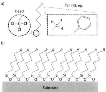
In order to achieve neutrality, it is possible to chemically modify this surface with a self-assembled monolayer (SAM)7. The native oxide surface of a Si wafer has higher SE (about 45 dynes cm-').
Therefore the native oxide surface is preferentially wetted by the PMMA-block of PS-b-PMMA, and is not neutral. A SAM, as shown in Figure 2.2, can be formed when a single-layer of short-chain molecules deposits on the substrate surface. The head of the molecule is one of the ends of the SAM that is able to chemically bond to the surface. The body of the molecule is the middle of the SAM and is typically a backbone of a 2-20 carbon atoms in length. The tail of the molecule (R) is the end opposite end of the
SAM which populates the air-interface to act as a new surface. For well-deposited SAMs, the molecules
chemically bond to the surface adjacent to each other, with high surface coverage, the molecules are oriented with the backbone of the SAM molecule perpendicular to the substrate surface and parallel to the adjacent molecule. The tails of the molecules populate the exposed top-surface of the monolayer (Figure
2.2b). For substrates modified with well-deposited SAMs, a uniform native oxide substrate surface can
adopt the characteristic surface chemistry of the new monolayer. 34
a) Tail (R): eg. Head H H Cl-Si-Cl H\ CI C H L --- --b) Si Si Si Si Si S s- S i S\ Si Si C( V o ( \C 0 0 / 0 /O \
Figure 2.2: Schematics of self-assembled monolayers. a)
Schematic of a trichlorosilane-based molecule for a self-assembled monolayer (SAM). The head is a trichlorosilane, attached to a carbon backbone. The reactive tail can be a number of different molecules, shown here with hydroxyl- and phenyl ring terminations. b) The head bonds to the silica-based substrate and many SAM molecules arrange to form an crystalline-ordered monolayer on the substrate surface.
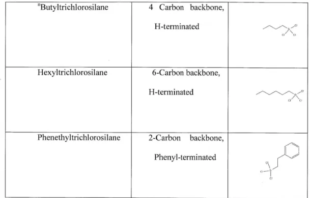
This study used a number of trichlorosilane-based SAMs which have been previously used for PS-b-PMMA self-assembly and they are listed in Table 2.18. "Butyltrichlorosilane (BTS) and Hexyltrichlorosilane (HTS) have hydrogen atoms as their terminating reactive species (R) and Phenethyltrichlorosilane (PTS) is terminated with a phenyl ring. SE measurements of these SAMs are reported and discussed below.
"Butyltrichlorosilane 4 Carbon backbone, H-terminated
Hexyltrichlorosilane 6-Carbon backbone, H-terminated
Phenethyltrichlorosilane 2-Carbon backbone, Phenyl-terminated
Table 2.1: List of the SAMs used in the presented results.
As discussed in Chapter 1, physical and chemical templates can be used to direct the self-assembly of BCPs. Publications have reported the separate employment of these two methods. When employed individually, each of the methods exhibits characteristic limitations. By developing a combined physical and chemical templating method, these characteristic limitations may be overcome. Furthermore, physical and chemically templating could contribute to the overall objectives and challenges of templated self-assembly of block copolymers. Although the work discussed in Chapter 2 focused on the separate development of these templating methods, this work was in preparation for the future combined method.
An example of the combined physical and chemical templating method is shown in Figure 2.3. In this case, an array of posts is fabricated on the substrate to act as a physical template. In conventional physical post templating, all of the posts are covered with a similar chemical modification such that they all have the same SE. In the combined method, the substrate is first chemically modified with a first SAM. The templating posts, comprised of a negative-tone resist hydrogen silsesquioxane (HSQ), are then fabricated
on top of this substrate. Then, the posts are chemically modified with a second SAM, which should not affect the first SAM. Consequently, the posts assume a different SE than the substrate, and can be used to combine physical and chemical templating.
SIDE VIEW: Second HSQ Posts on
First SAM SAM
SAM
Figure 2.3: Top- and side-view of an ideal example combined templating method. The substrate is modified with a first SAM (blue) to assume a first chemical nature. HSQ posts are then patterned on the SAM-coated substrate (grey). The HSQ posts are modified with a second SAM (red) to assume a second chemical nature. In this manner, both physical and chemical templating are combined.
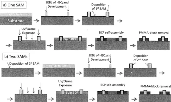
Figure 2.4 shows the major steps of the fabrication process. In some samples, only one SAM was deposited: HSQ physical post templates were first fabricated and then the SAM was deposited. In some samples, two SAMs were deposited: the first SAM was deposited, HSQ physical post templates fabricated, and then the second SAM deposited.
In order to produce HSQ physical template posts, a thin film of HSQ was first spun on the samples with no post-bake (thicknesses varied from 16 nm to 61 nm). Templates were exposed with scanning-electron-beam lithography (SEBL) on a Raith 150 (30keV, 30 gm objective aperture, 6mm working distance). After exposure, the samples were developed with a salty developer (4% NaCl / 1% NaOH in deionized water) at 24'C for 4 minutes and then rinsed with deionized water for 2 min and blown dry under N29. HSQ is a negative-tone resist, and therefore the unexposed resist is removed by the developer
solution. In certain experiments, SEBL exposure of the HSQ was "simulated". In these cases, HSQ was spun on the samples, stored in air for over 12 hours and developed as outlined above without electron-beam exposure via SEBL.
SAM deposition was initiated by soaking a prime Si wafer in a bath of CD26 (MICROPOSIT MF -CD-26 DEVELOPER, Dow Corning, Inc.), which contains a 2.5 wt. % tetramethylammonium hydroxide (TMAH) to fully hydroxyl-terminate the native silica surface. The wafer was rinsed with deionized water for 2 minutes, and blown dry under N2. A SAM solution was prepared by mixing 100 piL of the desired
SAM molecule (Gelest) in 100 mL toluene (J.T. Baker 99.9%) and matured for 10 minutes. The wafer
was immersed in this solution for 20 minutes to deposit the SAM, rinsed with toluene, and then blown dry under N2. Samples were baked on a hotplate at 120'C for 5 minutes. The ordering or crystallinity of the
deposited SAM was not determined.
Most of the samples were exposed to UV/Ozone for varying periods of time (conditions noted in results below).
- " -.- 1SEBL of HSQ and
a) One SAM evop Deposition
UV/Ozone
Ex osure BCP self-assembly PMMA-block removal
b) Two SAMS SEBL of HSQ and Deposition
.-- - Developmentl of 2nd SAM
Deposition of 1-t SAM
UV/Ozone
Exposure BCP self-assembly PMMA-block removal
Figure 2.4: Major steps of the fabrication process. (a) Steps when only a single SAM is to be deposited. (b) Steps when two different SAMs are to be deposited.
PS-b-PMMA (1.85 wt. % in 2-heptanone) was spin-coated on the samples at typical speeds of 1750-2500 rpm (60 sec, 10 acceleration (a.u.)) to produce thin films with thickness of 30-50 nm. The
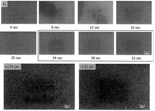
lamellae-forming PS-b-PMMA was purchased from Polymer Source (P2355, 98.2kg/mol, L. -45 nm). The remaining solvent after spin-coating was evaporated by baking the samples on a hot plate (130 C, 1 min). For thermal annealing, the oven was purged with N2 gas and then the heating elements turned on. The
desired temperature (about 220'C) was achieved after about 1.5 hours and the oven turned off after a total time of 2-2.5 hours. The oven was then left to cool to room temperature over the course of about 6 hours. The PMMA block of the polymer was removed by exposing the samples to 1 minute of UV/Ozone, then rinsing in acetic acid for 1 minute and deionized water for 1 minute.
In order to determine the SE characteristics of substrates, the contact angle of deionized water droplets was measured with a goniometer (model?) (as shown in Figure 2.5). Static, advancing, and receding contact angles of a water droplet dispensed from a syringe were measured. Each reported angle data point is an average of the contact angle on both sides of the water droplet at 3 different places on the sample, for a total of 6 angles. These data points were not used to compute the exact SE of samples, but only taken as measures of relative SE.
Figure 2.5: Microscope image of a water droplet on a sample in the goniometer. The syringe from the top dispenses the water onto the sample surface, and the microscope takes an image. This image is analyzed to determine the contact angle of the water on the surface.
Microscopy of samples was performed with a Raith 150 (10 keV, 30 im aperture, 6 mm working distance). As a result of the post-processing after BCP annealing, the PMMA-block was removed and high image contrast was achieved between the PS-block and the PMMA-voids.
2.2 Single-SAM Sample Modification for PS-b-PMMA Self-Assembly
For physical templating, HSQ posts were achieved on SAM-modified substrates. The fabrication of posts on a non-oxide substrate differed from previous results because physical post templates are typically fabricated on bare Si substrates0. With the objective of future application in combined physical and chemical template, posts were written in the process step after the first SAM deposition. This SAM-deposited substrate had a lower SE and therefore a higher likelihood of post collapse1 (lower adhesion of the post-base to the substrate), as is seen in Figure 2.6a. This effect was mitigated by reducing the HSQ resist thickness (hence post height) and therefore reducing torque on the post-base from the tall post (Figure 2.6b).
Figure 2.6: HSQ Posts fallen over and standing on a substrate. a) HSQ posts (white) are fallen over on the substrate due to capillary collapse. B) HSQ posts are standing on substrate surface, and therefore observed from the to-down as white dots. In this case, the thickness of the HSQ layer was lower, and therefore posts experienced